
The various paths to co-packaged optics

Near package optics has emerged as companies have encountered the complexities of co-packaged optics. It should not be viewed as an alternative to co-packaged optics but rather a pragmatic approach for its implementation.
Co-packaged optics will be one of several hot topics at the upcoming OFC show in March.
Placing optics next to silicon is seen as the only way to meet the future input-output (I/O) requirements of ICs such as Ethernet switches and high-end processors.
For now, pluggable optics do the job of routing traffic between Ethernet switch chips in the data centre. The pluggable modules sit on the switch platform’s front panel at the edge of the printed circuit board (PCB) hosting the switch chip.
But with switch silicon capacity doubling every two years, engineers are being challenged to get data into and out of the chip while ensuring power consumption does not rise.
One way to boost I/O and reduce power is to use on-board optics, bringing the optics onto the PCB nearer the switch chip to shorten the electrical traces linking the two.
The Consortium of On-Board Optics (COBO), set up in 2015, has developed specifications to ensure interoperability between on-board optics products from different vendors.
However, the industry has favoured a shorter still link distance, coupling the optics and ASIC in one package. Such co-packaging is tricky which explains why yet another approach has emerged: near package optics.
I/O bottleneck
“Everyone is looking for tighter and tighter integration between a switch ASIC, or ‘XPU’ chip, and the optics,” says Brad Booth, president at COBO and principal engineer, Azure hardware architecture at Microsoft. XPU is the generic term for an IC such as a CPU, a graphics processing unit (GPU) or even a data processing unit (DPU).
What kick-started interest in co-packaged optics was the desire to reduce power consumption and cost, says Booth. These remain important considerations but the biggest concern is getting sufficient bandwidth on and off these chips.
“The volume of high-speed signalling is constrained by the beachfront available to us,” he says.
Booth cites the example of a 16-lane PCI Express bus that requires 64 electrical traces for data alone, not including the power and ground signalling. “I can do that with two fibres,” says Booth.

Near package optics
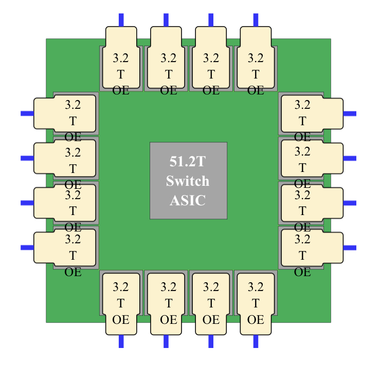
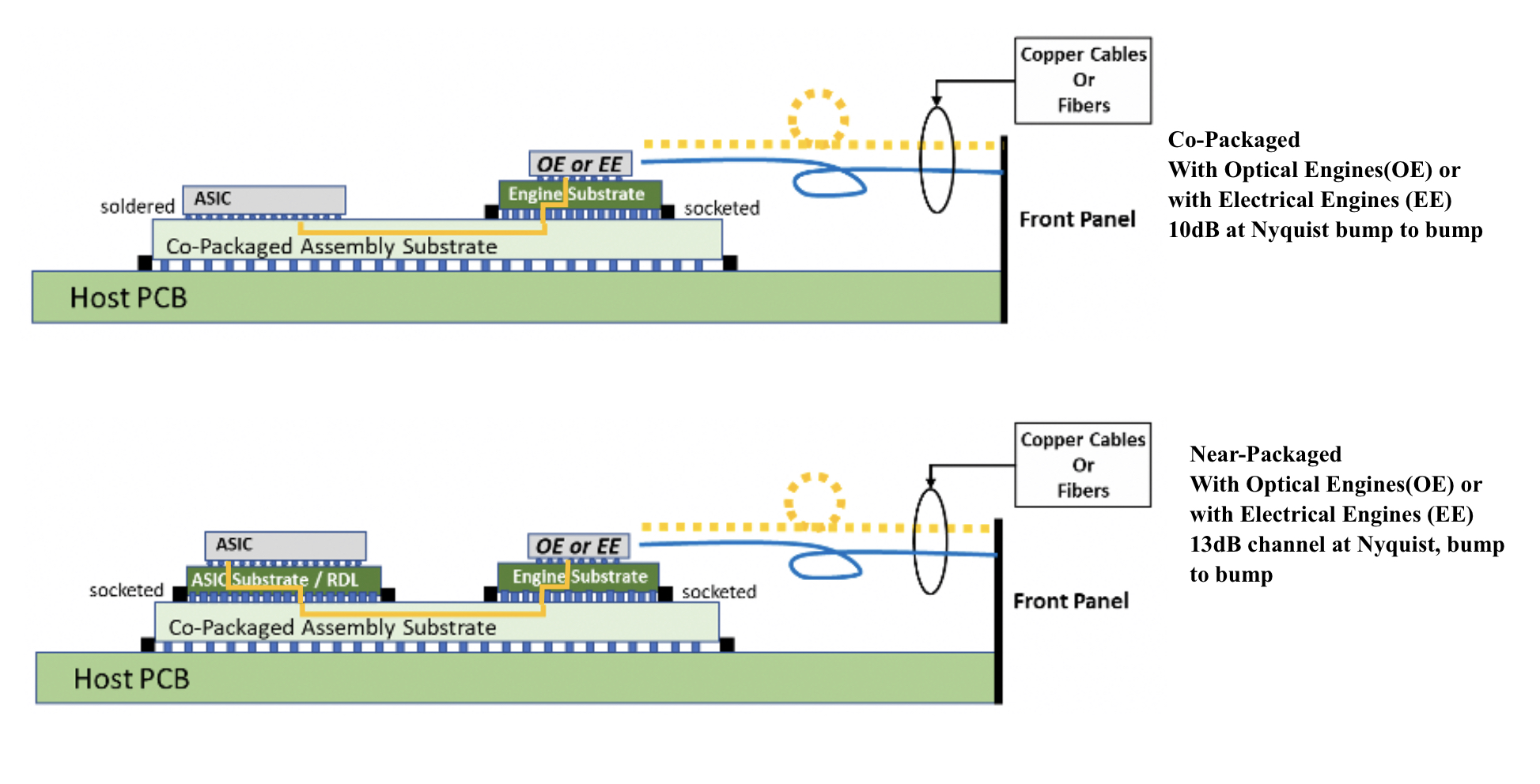
With co-packaged optics, the switch chip is typically surrounded by 16 optical modules, all placed on an organic substrate (see diagram below).
“Another name for it is a multi-chip module,” says Nhat Nguyen, senior director, solutions architecture at optical I/O specialist, Ayar Labs.
A 25.6-terabit Ethernet switch chip requires 16, 1.6 terabits-per-second (1.6Tbps) optical modules while upcoming 51.2-terabit switch chips will use 3.2Tbps modules.
“The issue is that the multi-chip module can only be so large,” says Nguyen. “It is challenging with today’s technology to surround the 51.2-terabit ASIC with 16 optical modules.”
Near package optics tackles this by using a high-performance PCB substrate – an interposer – that sits on the host board, in contrast to co-packaged optics where the modules surround the chip on a multi-chip module substrate.
The near package optics’ interposer is more spacious, making the signal routing between the chip and optical modules easier while still meeting signal integrity requirements. Using the interposer means the whole PCB doesn’t need upgrading which would be extremely costly.
Some co-packaged optics design will use components from multiple suppliers. One concern is how to service a failed optical engine when testing the design before deployment. “That is one reason why a connector-based solution is being proposed,” says Booth. “And that also impacts the size of the substrate.”

A larger substrate is also needed to support both electrical and optical interfaces from the switch chip.
Platforms will not become all-optical immediately and direct-attached copper cabling will continue to be used in the data centre. However, the issue with electrical signalling, as mentioned, is it needs more space than fibre.
“We are in a transitional phase: we are not 100 per cent optics, we are not 100 per cent electrical anymore,” says Booth. “How do you make that transition and still build these systems?”
Perspectives
Ayar Labs views near package optics as akin to COBO. “It’s an attempt to bring COBO much closer to the ASIC,” says Hugo Saleh, senior vice president of commercial operations and managing director of Ayar Labs U.K.
However, COBO’s president, Booth, stresses that near package optics is different from COBO’s on-board optics work.
“The big difference is that COBO uses a PCB motherboard to do the connection whereas near package optics uses a substrate,” he says. “It is closer than where COBO can go.”
It means that with near package optics, there is no high-speed data bandwidth going through the PCB.
Booth says near package optics came about once it became obvious that the latest 51.2-terabit designs – the silicon, optics and the interfaces between them – cannot fit on even the largest organic substrates.
“It was beyond the current manufacturing capabilities,” says Booth. “That was the feedback that came back to Microsoft and Facebook (Meta) as part of our Joint Development Foundation.”
Near package optics is thus a pragmatic solution to an engineering challenge, says Booth. The larger substrate remains a form of co-packaging but it has been given a distinct name to highlight that it is different to the early-version approach.
Nathan Tracy, TE Connectivity and the OIF’s vice president of marketing, admits he is frustrated that the industry is using two terms since co-packaged optics and near package optics achieve the same thing. “It’s just a slight difference in implementation,” says Tracy.
The OIF is an industry forum studying the applications and technology issues of co-packaging and this month published its framework Implementation Agreement (IA) document.
COBO is another organisation working on specifications for co-packaged optics, focussing on connectivity issues.
Technical differences
Ayar Labs highlights the power penalty using near package optics due to its use of longer channel lengths.
For near package optics, lengths between the ASIC and optics can be up to 150mm with the channel loss constrained to 13dB. This is why the OIF is developing the XSR+ electrical interface, to expand the XSR’s reach for near package optics.
In contrast, co-packaged optics confines the modules and host ASIC to 50mm of each other. “The channel loss here is limited to 10dB,” says Nguyen. Co-packaged optics has a lower power consumption because of the shorter spans and 3dB saving.
Ayar Labs highlights its optical engine technology, the TeraPHY chiplet that combines silicon photonics and electronics in one die. The optical module surrounding the ASIC in a co-packaged design typically comprises three chips: the DSP, electrical interface and photonics.
“We can place the chiplet very close to the ASIC,” says Nguyen. The distance between the ASIC and the chiplet can be as close as 3-5mm. Whether on the same interposer Ayar Labs refers to such a design using athird term: in-package optics.
Ayar Labs says its chiplet can also be used for optical modules as part of a co-packaged design.
The very short distances using the chiplet result in a power efficiency of 5pJ/bit whereas that of an optical module is 15pJ/bit. Using TeraPHY for an optical module co-packaged design, the power efficiency is some 7.5pJ/bit, half that of a 3-chip module.
A 3-5mm distance also reduces the latency while the bandwidth density of the chiplet, measured in Gigabit/s/mm, is higher than the optical module.
Co-existence
Booth refers to near package optics as ‘CPO Gen-1’, the first generation of co-packaged optics.
“In essence, you have got to use technologies you have in hand to be able to build something,” says Booth. “Especially in the timeline that we want to demonstrate the technology.”
Is Microsoft backing near package optics?

“We are definitely saying yes if this is what it takes to get the first level of specifications developed,” says Booth.
But that does not mean the first products will be exclusively near package optics.
“Both will be available and around the same time,” says Booth. “There will be near packaged optics solutions that will be multi-vendor and there will be more vertically-integrated designs; like Broadcom, Intel and others can do.”
From an end-user perspective, a multi-vendor capability is desirable, says Booth.
Ayar Labs’ Saleh sees two developing paths.
The first is optical I/O to connect chips in a mesh or as part of memory semantic designs used for high-performance computing and machine learning. Here, the highest bandwidth and lowest power are key design goals.
Ayar Labs has just announced a strategic partnership with high performance computing leader, HPE, to design future silicon photonics solutions for HPE’s Slingshot interconnect that is used for upcoming Exascale supercomputers and also in the data centre.
The second path concerns Ethernet switch chips and here Saleh expects both solutions to co-exist: near package optics will be an interim solution with co-packaged optics dominating longer term. “This will move more slowly as there needs to be interoperability and a wide set of suppliers,” says Saleh.
Booth expects continual design improvements to co-packaged optics. Further out, 2.5D and 3D chip packaging techniques, where silicon is stacked vertically, to be used as part of co-packaged optics designs, he says.
Preparing for a post-pluggable optical module world

Part 1: OIF: ELSFP, XSR+, and CEI-112G-Linear
The OIF is working on several electrical and optical specifications as the industry looks beyond pluggable optical transceivers.
One initiative is to specify the external laser source used for co-packaged optics, dubbed the External Laser Small Form Factor Pluggable (ELSFP) project.
Industry interest in co-packaged optics, combining an ASIC and optical chiplets in one package, is growing as it becomes increasingly challenging and costly to route high-speed electrical signals between a high-capacity Ethernet switch chip and the pluggable optics on the platform’s faceplate.
The OIF is also developing 112-gigabit electrical interfaces to address not just co-packaged optics but also near package optics and the interface needs of servers and graphics processor units (GPUs).
Near package optics also surrounds the ASIC with optical chiplets. But unlike co-packaged optics, the ASIC and chiplets are placed on a high-performance substrate located on the host board.
ELSFP
Data centre operators have vast experience using pluggables and controlling their operating environment so that they don’t overheat. The thermal management of optics co-packaged with an ASIC that can dissipate hundreds of watts is far trickier.
“Of all the components, the one that hates heat the most is the laser,” says Nathan Tracy, TE Connectivity and the OIF’s vice president of marketing.
Players such as Intel and Juniper have integrated laser technology, allowing them to place the full transceiver on a chip. However, the industry trend is to use an external light source so that the laser is decoupled from the remaining optical transceiver circuitry.
“We bring fibre into and out of the co-packaged optical transceiver so why not add a couple more fibres and bring the laser source into the transceiver as well?” says Tracy.
Two approaches are possible. One is to box the lasers and place them within the platform in a thermally-controlled environment. Alternatively, the lasers can be boxed and placed on the equipment’s faceplate, as pluggable optics are today.
“We know how to do that,” says Tracy. “But it is not a transceiver, it is a module full of lasers.”
Such a pluggable laser approach also addresses a concern of the data centre operators: how to service the optics of a co-packaged design.
The OIF’s ELSFP project is working to specify such a laser pluggable module: its mechanical form factor, electrical interface, how light will exit the module, and its thermal management.
The goal is to develop a laser pluggable that powers up when inserted and has a blind-mate optical interface, ensuring light reaches the co-packaged optics transceivers on the host board with minimal optical loss.
“Optical interfaces are fussy things,” says Tracy. Such interfaces must be well-aligned, clean, and hold tight tolerances, says Tracy: “That is all captured under the term blind-mate.”
Optical fibre will deliver light from the laser module to the co-packaged optics but multi-core fibre may be considered in future.
One issue the OIF is discussing is the acceptable laser output power. The higher the output power, the more the source can be split to feed more co-packaged optics transceivers. But higher-power lasers have eye-safety issues.
Another topic being addressed is the fibre density the form factor should enable. The OIF wants a roadmap to ensure that future co-packaged optics’ needs are also met.
“The industry can then take that specification and go compete in the market, adding their differentiation on top of the standardisation,” says Tracy.
The OIF’s ELSFP members have submitted technical contributions and a draft specification exists. “Now we are in the iterative process with members building on that draft,” says Tracy.
Co-packaged optics and near package optics
As the capacity of switch chips continues to double, more interfaces are needed to get data in and out and the harder it is becoming to route the channels between the chip and the optical modules.
The chip package size is also increasing with the growing aggregate bandwidth and channels, says Tracy. These channels come out via the package’s solder balls that connect to the host board.
“You don’t want to make that ASIC package any bigger than it needs to be; packages have bad parasitics,” says Tracy
For a fully co-packaged design, a switch ASIC is surrounded by 16 optical engines. For next-generation 51.2-terabit switch ASICs, 3.2 terabits-per-second (Tbps) optical engines will be required. Add the optical engines and the switch package becomes even bigger.
“You are starting to get to the point where you are making the package bigger in ways that are challenging the industry,” says Tracy.
Near package optics offers an alternative approach to avoid cramming the optics with the ASIC. Here, the ASIC and the chiplets are mounted on a high-performance substrate that sits on the host card.
“Now the optical engines are a little bit further away from the switching silicon than in the co-packaged optics’ case,” says Tracy.
CEI-112G-Extra Short Reach Plus (XSR+) electrical interface
According to optical I/O specialist, Ayar Labs, near package optics and co-packaged optics have similar optical performance given the optical engines are the same. Where they differ is the electrical interface requirements.
With co-packaged optics, the channel length between the ASIC and the optical engine is up to 50mm and the channel loss is 10dB. With near package optics, the channel length is up to 150mm and a 13dB channel loss.
The OIF’s 112Gbps XSR+ electrical interface is to meet the longer reach needs of near package optics.
“It enables a little bit more margin or electrical channel reach while being focused on power reduction,” says Tracy. “Co-packaged optics is all about power reduction; that is its value-add.”
CEI-112G-Linear
A third ongoing OIF project – the CEI-112-Linear project – also concerns a 112Gbps chip-to-optical engine interface.
The project’s goal is to specify a linear channel so that the chip’s electrical transmitter (serdes) can send data over the link – made up of an optical transmitter and an optical receiver as well as the electrical receiver at the far end – yet requires equalisation for the transmitter and end receiver only.
“A linear link means we understand the transition of the signal from electrical to optical to electrical,” says Tracy. “If we are operating over a linear range then equalisation is straightforward.” That means simpler processing for the signal’s recovery and an overall lower power consumption.
By standardising such a linear interface, multiple chip vendors will be able to drive the optics of multiple I/O chiplet companies.
“Everything is about power savings, and the way to get there is by optimising the link,” says Tracy.
224-gigabit electrical interfaces
The OIF’s next-generation 224Gbps electrical interface work continues to progress. Member input to date has tackled the challenges, opportunities and the technologies needed to double electrical interface speeds.
“We are surveying the playing field to understand where the really hard parts are,” says Tracy.
A White Paper is expected in the coming year that will capture how the industry views the issues and the possible solutions.
“If you have industry consensus then it is easier to start a project addressing the specific implementation to meet the problem,” says Tracy.
The OIF’s 400ZR coherent interface starts to take shape
Part 2: Coherent developments
The Optical Internetworking Forum’s (OIF) group tasked with developing two styles of 400-gigabit coherent interface is now concentrating its efforts on one of the two.
When first announced last November, the 400ZR project planned to define a dense wavelength-division multiplexing (DWDM) 400-gigabit interface and a single wavelength one. Now the work is concentrating on the DWDM interface, with the single-channel interface deemed secondary.
 Karl Gass"It [the single channel] appears to be a very small percentage of what the fielded units would be,” says Karl Gass of Qorvo and the OIF Physical and Link Layer working group vice chair, optical, the group responsible for the 400ZR work.
The likelihood is that the resulting optical module will serve both applications. “Realistically, probably both [interfaces] will use a tunable laser because the goal is to have the same hardware,” says Gass.
The resulting module may also only have a reach of 80km, shorter than the original goal of up to 120km, due to the challenging optical link budget.
Origins and status
The 400ZR project began after Microsoft and other large-scale data centre players such as Google and Facebook approached the OIF to develop an interoperable 400-gigabit coherent interface they could then buy from multiple optical module makers.
The internet content providers’ interest in an 80km-plus link is to connect premises across the metro. “Eighty kilometres is the magic number from a latency standpoint so that multiple buildings can look like a single mega data centre,” says Nathan Tracy of TE Connectivity and the OIF’s vice president of marketing.
Since then, traditional service providers have shown an interest in 400ZR for their metro needs. The telcos’ requirements are different to the data centre players, causing the group to tweak the channel requirements. This is the current focus of the work, with the OIF collaborating with the ITU.
The catch is how much can we strip everything down and still meet a large percentage of the use cases
“The ITU does a lot of work on channels and they have a channel measurement methodology,” says Gass. “They are working with us as we try to do some division of labour.”
The group will choose a forward error correction (FEC) scheme once there is common agreement on the channel. “Imagine all those [coherent] DSP makers in the same room, each one recommending a different FEC,” says Gass. “We are all trying to figure out how to compare the FEC schemes on a level playing field.”
Meeting the link budget is challenging, says Gass, which is why the link might end up being 80km only. “The catch is how much can we strip everything down and still meet a large percentage of the use cases.”
The cloud is the biggest voice in the universe
400ZR form factors
Once the FEC is chosen, the power envelope will be fine-tuned and then the discussion will move to form factors. The OIF says it is still too early to discuss whether the project will select a particular form factor. Potential candidates include the OSFP MSA and the CFP8.
 Nathan TracyThe industry assumption is that the 80km-plus 400ZR digital coherent optics module will consume around 15W, requiring a very low-power coherent DSP that will be made using 7nm CMOS.
“There is strong support across the industry for this project, evidenced by the fact that project calls are happening more frequently to make the progress happen,” says Tracy.
Why the urgency? “The cloud is the biggest voice in the universe,” says Tracy. To support the move of data and applications to the cloud, the infrastructure has to evolve, leading to the data centre players linking smaller locations spread across the metro.
“At the same time, the next-gen speed that is going to be used in these data centres - and therefore outside the data centres - is 400 gigabit,” says Tracy.
Micro QSFP module to boost equipment port densities
 Nathan Tracy
The μQSFP will support both copper and optical cabling, and will have an improved thermal performance, benefitting interfaces and platforms.
“There is always a quest for greater port density or aggregate bandwidth,” says Nathan Tracy, technologist at TE Connectivity and chair of the μQSFP MSA.
The challenge for the module makers is to provide denser form factors to increase overall system traffic. “As we go to higher densities, we are also increasing the thermal load,” says Tracy. “And so now it is a mechanical and a thermal [design] problem, and both need to be solved jointly.”
The thermal load is increased since the μQSFP supports interfaces that consume up to 3.5 W - like the QSFP - while having the width of the smaller SFP rated at 1.5 W.
“We are limited in the directions we can pull the heat out,” says Tracy. “If we are going to enable a higher density form factor that has the same width as an SFP but it is going to have the functionality of a QSFP, now we have a problem.”
This requires the MSA engineers to develop new ways to rid the μQSFP of its heat.
If we are going to enable a higher density form factor that has the same width as an SFP but it is going to have the functionality of a QSFP, now we have a problem
Heat transfer and other challenges
The volume and surface area of a module determine the overall thermal capacity or thermal density. The module can be modelled as an electrical circuit, with heat flow equivalent to current, while each interface has a thermal resistance.
There are three interfaces - thermal resistances - associated with a module: between the heat source and the module case, the case and the heat sink, and the heat sink and ambient air. These three thermal resistances are in series and the goal is to reduce them to ensure greater heat flow.
The module’s circuitry generates heat and the interface between the circuitry and the module’s case is one of the thermal resistances. “You are going to have a heat source in the module and no matter what you do, there is going to be some thermal resistance from that source to the module housing,” says Tracy.
You have to get good signal integrity through that electrical interface because we are working at 25 gigabit-per-second (Gbps) data rates today and we know 50 Gbps data rates are coming
The second thermal resistance - one that the µQSFP eliminates - is between the module housing and the heat sink. Sliding a module into its cage puts it into contact with the heat sink. But the contact between the two surfaces is imperfect, making heat extraction harder. Building the heat sink into the μQSFP module avoids using the sliding design.
The remaining thermal resistance is between the heat sink and the cooling air blown through the equipment. This thermal resistance between the heat sink's metal fin structure and the air flow exists however good the heat sink design, says Tracy.
Other design challenges include achieving signal integrity when cramming the four electrical lanes across the µQSFP’s smaller width, especially when its support 25 Gbit/s lanes and likely 50 Gbit/s in future, says Tracy.
And the module's optical interface must also support duplex LC and MPO connectors to interoperate with existing cabling.
“It is all a balancing act,” says Tracy.
Applications
The μQSFP is aimed at platforms such as 4.8 and 6.4 Tbps capacity switches. The QSFP is used for current 3.2 Tbps platforms but greater port densities will be needed for these next-generation platforms. The size of the μQSFP means 48 ports will fit in the space 36 QSFPs currently occupy, while 72 μQSFPs will fit on a line card if three rows are used.
The μQSFP may also find use outside the data centre for longer, 100 km reaches. “Today you can buy SFP modules that go 100 km,” says Tracy. “With this form factor, we are creating the capability to go up to four lanes in the same width as an SFP and, at the same time, we are improving the thermal performance significantly over what an SFP can do.”
The Micro QSFP group is not saying when the µQSFP MSA will be done. But Tracy believes the μQSFP would be in demand were it available now. Its attraction is not just the greater port density, but how the µQSFP would aid systems engineers in tackling their thermal design challenges.
The pluggable form factor will allow air to flow from the face plate and through the module to where ICs and other circuitry reside. Moreover, since 32 μQSFP ports will take up less face-plate area than 32 QSFPs, perforations could be added, further improving airflow.
“If you look at the QSFP or SFP, it does not allow airflow through the cage from the front [plate] to the back,” says Tracy.
The μQSFP MSA founding members are Avago Technologies, Broadcom, Brocade, Cisco, Dell, Huawei, Intel, Lumentum (formerly JDSU), Juniper Networks, Microsoft, Molex, and TE Connectivity.
OIF shows 56G electrical interfaces & CFP2-ACO
“The most important thing for everyone is power consumption on the line card”
The OIF - an industry organisation comprising communications service providers, internet content providers, system vendors and component companies - is developing the next common electrical interface (CEI) specifications. The OIF is also continuing to advance fixed and pluggable optical module specifications for coherent transmission including the pluggable CFP2 (CFP2-ACO).
“These are major milestones that the [demonstration] efforts are even taking place,” says Nathan Tracy, a technologist at TE Connectivity and the OIF technical committee chair.
Tracy stresses that the CEI-56G specifications and the CFP2-ACO remain works in progress. “They are not completed documents, and what the demonstrations are not showing are compliance and interoperability,” he says.
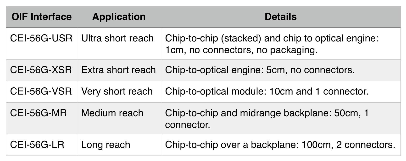
Five CEI-56G specifications are under development, such as platform backplanes and links between a chip and an optical engine on a line card (see Table below).
Moving from the current 28 Gig electrical interface specifications to 56 Gig promises to double the interface capacity and cut electrical interface widths by half. “If we were going to do 400 Gigabit with 25 Gig channels, we would need 16 channels,” says Tracy. “If we can do 50 Gig, we can get it down to eight channels.” Such a development will enable chassis to carry more traffic and help address the continual demand for more bandwidth, he says.
But doubling the data rate is challenging. “As we double the rate, the electrical loss or attenuation of the signal travelling across a printed circuit board is significantly impacted,” says Tracy. “So now our reaches have to get a lot shorter, or the silicon that sends and receives has to improve to significant higher levels.”
One of the biggest challenges in system design is thermal management
Moreover, chip designers must ensure that the power consumption of their silicon do not rise. “We have to be careful as to what the market will tolerate, as one of the biggest challenges in system design is thermal management,” says Tracy. “We can’t just do what it takes to get to 56 Gigabit.”
To this aim, the OIF is pursuing two parallel tracks: using 56 Gigabit non-return-to-zero (NRZ) signalling and 4-level pulse amplitude modulation (PAM-4) which encodes two bits per symbol such that a 28 Gbaud signalling rate can be used. The 56 Gig NRZ uses simpler signalling but must deal with the higher associated loss, while PAM-4 does not suffer the same loss as it is similar to existing CEI-28 channels used today but requires a more complex design.
“Some [of the five CEI-56G specifications] use NRZ, some PAM-4 and some both,” says Tracy. The OIF will not say when it will complete the CEI-56G specifications. However, the projects are making similar progress while the OIF is increasing its interactions with other industry standards groups to shorten the overall timeline.
 Source: OIF, Gazettabyte
Two of the CEI-56G specifications cover much shorter distances: the Extra Short Reach (XSR) and Ultra Short Reach (USR). According to the OIF, in the past it was unclear that the industry would benefit from interoperability for such short reaches.
“What is different at 56 Gig is that architectures are fundamentally being changed: higher data rates, industry demand for higher levels of performance, and changing fabrication technologies,” says Tracy. Such fabrication technologies include 3D packaging and multi-chip modules (MCMs) where silicon dies from different chip vendors may be connected within the module.
The XSR interface is designed to enable higher aggregate bandwidth on a line card which is becoming limited by the number of pluggable modules that can be fitted on the platform’s face plate. Density can be increased by using mid-board optics (an optical engine) placed closer to a chip. Here, fibre from the optical engine is fed to the front plate increasing the overall interface capacity.
The USR interface is to support stackable ICs and MCMs.
All are coming together in this pre-competitive stage to define the specifications, yet, at the same time, we are all fierce competitors
“The most important thing for everyone is power consumption on the line card,” says Tracy. “If you define these very short reach interfaces in such a way that these chips do not need as much power, then we have helped to enable the next generation of line card.”
The live demonstrations at OFC include a CEI-56G-VSR-NRZ channel, a CEI-56G-VSR-PAM QSFP compliance board, CEI-56G-MR/LR-PAM and CEI-56G-MR/LR-NRZ backplanes, and a CEI-56G-MR-NRZ passive copper cable.
The demonstrations reflects what OIF members are willing to show, as some companies prefer to keep their work private. “All are coming together in this pre-competitive stage to define the specifications, yet, at the same time, we are all fierce competitors,” says Tracy.
CFP2-ACO
Also on display is working CFP2 analogue coherent optics (CFP2-ACO). The significance of coherent optics in a pluggable CFP2 is the promise of higher-density line cards. The CFP is a much bigger module and at most four can be fitted on a line card, while with the smaller CFP2, with its lower power consumption, up to eight modules are possible.
Using the CFP2-ACO, the coherent DSP-ASIC is external to the CFP2 module. Much work has been done to ensure that the electrical interface can support the analogue signalling between the CFP2 optics and the on-board DSP-ASIC, says Tracy.
At OFC, several companies have unveiled their CFP2-ACO products including Finisar, Fujitsu Optical Components, Oclaro and NEC, while Clariphy has announced a single-board reference design that includes its CL20010 DSP-ASIC and a CFP2-ACO slot.