
Broadcom's first Jericho3 takes on AI's networking challenge
Add Content
Broadcom’s Jericho silicon has taken an exciting turn.
The Jericho devices are used for edge and core routers.
But the first chip of Broadcom’s next-generation Jericho is aimed at artificial intelligence (AI); another indicator, if one is needed, of AI’s predominance.
Dubbed the Jericho3-AI, the device networks AI accelerator chips that run massive machine-learning workloads.
AI supercomputers
AI workloads continue to grow at a remarkable rate.
The most common accelerator chip used to tackle such demanding computations is the graphics processor unit (GPU).
GPUs are expensive, so scaling them efficiently is critical, especially when AI workloads can take days to complete.
“For AI, the network is the bottleneck,” says Oozie Parizer, (pictured) senior director of product management, core switching group at Broadcom.
Squeezing more out of the network equates to shorter workload completion times.
“This is everything for the hyperscalers,” says Parizer. “How quickly can they finish the job.”
Broadcom shares a chart from Meta (below) showing how much of the run time for its four AI recommender workloads is spent on networking, moving the data between the GPUs.

In the worse case, networking accounts for three fifths (57 per cent) of the time during which the GPUs are idle, waiting for data.
Scaling
Parizer highlights two trends driving networking for AI supercomputers.
One is the GPU’s growing input-output (I/O), causing a doubling of the interface speed of network interface cards (NICs). The NIC links the GPU to the top-of-rack switch.
The NIC interface speeds have progressed from 100 to 200 to now 400 gigabits and soon 800 gigabits, with 1.6 terabits to follow.
The second trend is the amount of GPUs used for an AI cluster.
The largest cluster sizes have used 64 or 256 GPUs, limiting the networking needs. But now machine-learning tasks require clusters of 1,000 and 2,000 GPUs up to 16,000 and even 32,000.
Meta’s Research SuperCluster (RSC), one of the largest AI supercomputers, uses 16,000 Nvidia A100 GPUs: 2,000 Nvidia DGX A100 systems each with eight A100 GPUs. The RSC also uses 200-gigabit NICs.
“The number of GPUs participating in an all-to-all exchange [of data] is growing super fast,” says Parizer.
The Jericho3-AI is used in the top-of-rack switch that connects a rack’s GPUs to other racks in the cluster.
The Jericho3-AI enables clusters of up to 32,000 GPUs, each served with an 800-gigabit link.
An AI supercomputer can used all its GPUs to tackle one large training job or split the GPUs into pools running AI workloads concurrently.
Either way, the cluster’s network must be ‘flat’, with all the GPU-to-GPU communications having the same latency.
Because the GPUs exchange machine-learning training data in an all-to-all manner, only when the last GPU receives its data can the computation move onto the next stage.
“The primary benefit of Jericho3-AI versus traditional Ethernet is predictable tail latency,” says Bob Wheeler, principal analyst at Wheeler’s Network. “This metric is very important for AI training, as it determines job-completion time.”
Data spraying
“We realised in the last year that the premium traffic capabilities of the Jericho solution are a perfect fit for AI,” says Parizer.
The Jericho3-AI helps maximise GPU processing performance by using the full network capacity while traffic routing mechanisms help nip congestion in the bud.
The Jericho also adapts the network after a faulty link occurs. Such adaptation must avoid heavy packet loss otherwise the workload must be restarted, potentially losing days of work.
AI workloads use large packet streams known as ‘elephant’ flows. Such flows tie up their assigned networking path, causing congestion when another flow also needs that path.
“If traffic follows the concept of assigned paths, there is no way you get close to 100 per cent network efficiency,” says Parizer.
The Jericho3-AI, used in a top-of-rack switch, has a different approach.
Of the device’s 28.8 terabits of capacity, half connects the rack’s GPUs’ NICs and a half to the ‘fabric’ that links the rack’s GPUs to all the other cluster’s GPUs.
Broadcom uses the 14.4-terabit fabric link as one huge logical pipe over which traffic is evenly spread. Each destination Jericho3-AI top-of-rack switch then reassembles the ‘sprayed’ traffic.
“From the GPU’s perspective, it is unaware that we are spraying the data,” says Parizer.
Receiver-based flow control
Spraying may ensure full use of the network’s capacity, but congestion can still occur. The sprayed traffic may be spread across the fabric to all the spine switches, but for short periods, several GPUs may send data to the same GPU, known as incast (see diagram).

The Jericho copes with this many-to-one GPU traffic using receiver-based flow control.
Traffic does not leave the receiving Jericho chip just because it has arrived, says Parizer. Instead, the receiving Jericho tells the GPUs with traffic to send and schedules part of the traffic from each.
“Traffic ends up queueing nearer the sender GPUs, notifying each of them to send a little bit now, and now,” says Parizer, who stresses this many-to-one condition is temporary.
Ethernet flow control is used when Jericho chip senses that too much traffic is being sent.
“There is a temporary stop in data transmission to avoid packet loss in network congestion,” says Parizer. “And it is only that GPU that needs to slow down; it doesn’t impact any adjacent GPUs.”
Fault control
At Optica’s Executive Forum event, held alongside the OFC show in March, Google discussed using a 6,000 tensor processor unit (TPU) accelerator system to run large language models.
One Google concern is scaling such clusters while ensuring overall reliability and availability, given the frailty of large-scale accelerator clusters.
“With a huge network having thousands of GPUs, there is a lot of fibre,” says Parizer. “And because it is not negligible, faults happen.”
New paths must be calculated when an optical link goes down in a network arrangement that using flows and assigned paths with significant traffic loss likely.
“With a job that has been running for days, significant packet loss means you must do a job restart,” says Parizer.
Broadcom’s solution, not based on flows and assigned paths, uses load balancing to send data over one less path overall.
Using the Jericho2C+, Broadcom has shown fault detection and recovery in microseconds such that the packet loss is low and no job restart is needed.
The Jericho portfolio of devices
Broadcom’s existing Jericho2 architecture combines an enhanced packet-processing pipeline with a central modular database and a vast memory holding look-up tables.
Look-up tables are used to determine how the packet is treated: where to send it, wrapping it in another packet (tunnel encapsulation), extracting it (tunnel termination), and access control lists (ACLs).
Different stages in the pipeline can access the central modular database, and the store can be split flexibly without changing the packet-processing code.
Jericho2 was the first family device with a 4.8 terabit capacity and 8 gigabytes of high bandwidth memory (HBM) for deep buffering.
The Jericho 2C followed, targeting the edge and service router market. Here, streams have lower bandwidth – 1 and 10 gigabits typically – but need better support in the form of queues, counters and metering, used for controlling packets and flows.
Pariser says the disaggregated OpenBNG initiative supported by Deutsche Telekom uses the Jericho 2C.
Broadcom followed with a third Jericho2 family device, the Jericho 2C+, which combines the attributes of Jericho2 and Jericho2C.
Jericho2C+ has 14.4 terabits of capacity and 144 100-gigabit interfaces, of which 7.2-terabit is network interfacing bandwidth and 7.2-terabit for the fabric interface.
“The Jericho2C+ is a device that can target everything,” says Pariser.
Applications include data centre interconnect, edge and core network routing, and even tiered switching in the data centre.
Hardware design
The Jericho3-AI, made up of tens of billions of transistors in a 5nm CMOS process, is now sampling.
Broadcom says it designed the chip to be cost-competitive for AI.
For example, the packet processing pipeline is simpler than the one used for core and edge routing Jericho.
“This also translates to lower latency which is something hyperscalers also care about,” says Parizer.
The cost and power savings from optimisations will be relatively minor, says Wheeler.

Broadcom also highlights the electrical performance of the Jericho3-AI’s input-output serialiser-deserialiser (serdes) interfaces.
The serdes allows the Jericho3-AI to be used with 4m-reach copper cables linking the GPUs to the top-of-rack switch.
The serdes performance also enables linear-drive pluggables that dont have no digital signal processor (DSP) for retiming with the serdes driving the pluggable directly. Linear drive saves cost and power.
Broadcom’s Ram Valega, senior vice president and general manager of the core switching group, speaking at the Open Compute Project’s regional event held in Prague in April, said 32,000 GPU AI clusters cost around $1 billion, with 10 per cent being the network cost.

Valega showed Ethernet outperforms Infiniband by 10 per cent for a set of networking benchmarks (see diagram above).
“If I can make a $1 billion system ten per cent more efficient, the network pays for itself,” says Valega.
Wheeler says the comparison predates the recently announced NVLink Network, which will first appear in Nvidia’s DGX GH200 platform.
“It [NVLink Network] should deliver superior performance for training models that won’t fit on a single GPU, like large language models,” says Wheeler.

Enfabrica’s chip tackles AI supercomputing challenges
- Enfabrica’s accelerated compute fabric chip is designed to scale computing clusters comprising CPUs and specialist accelerator chips.
- The chip uses memory disaggregation and high-bandwidth networking for accelerator-based servers tackling artificial intelligence (AI) tasks.
For over a decade, cloud players have packed their data centres with x86-based CPU servers linked using tiers of Ethernet switches.
“The reason why Ethernet networking has been at the core of the infrastructure is that it is incredibly resilient,” says Rochan Sankar, CEO and co-founder of Enfabrica.
But the rise of AI and machine learning is causing the traditional architecture to change.
What is required is a mix of processors: CPUs and accelerators. Accelerators are specialist processors such as graphics processing units (GPUs), programmable logic (FPGAs), and custom ASICs developed by the hyperscalers.
It is the accelerator chips, not the CPUs, that do the bulk of the processing. Accelerators also require vast data, creating challenging input-output (I/O) and memory requirements.
At Optica’s Executive Forum event, held alongside the OFC show in March, Ryohei Urata, director and principal engineer at Google, mentioned how Google uses two computing pods – comprising 6,000 TPU accelerators – to run its large language models.
A key concern for Google is scaling such clusters while ensuring their reliability and availability. It is critical that the system is available when running a large language model, says Urata,
“As an engineer, when you’re putting stuff down, at least when you’re first start to put it together, you think, okay, this is going to work perfectly,” says Urata. “This is a perfect design, you don’t factor in failing gracefully, so that’s a key lesson.”
Google’s concern highlights that accelerator-based clusters lack the reliability of data centre server-Ethernet networks.
Accelerated compute fabric
Start-up Enfabrica has developed a chip, dubbed the accelerated compute fabric, to scale computing clusters.
“The focus of Enfabrica is on how networking and fabric technologies have to evolve in the age of AI-driven computing,” says Sankar.
AI models are growing between 8x to 275x annually, placing enormous demands on a data centre’s computing and memory resources.
“Two hundred and seventy-five times are of the order of what the large language models are increasing by, 8x is more other models including [machine] vision; recommender models are somewhere in between,” says Sankar.
Another AI hardware driver is growing end-user demand; ChatGPT gained 100 million users in the first months after its launch.
Meeting demand involves cascading more accelerators but the I/O bandwidth connected to the compute is lagging. Moreover, that gap is growing.
Sankar includes memory bandwidth as part of the I/O issue and segments I/O scaling into two: connecting CPUs, GPUs, accelerators and memory in the server, and the I/O scaling over the network.
A computing architecture for AI must accommodate greater CPUs and accelerators yet tackle the I/O bottleneck.
“To scale, it requires disaggregation; otherwise, it becomes unsustainable and expensive, or it can’t scale enough to meet processing demands,” says Sankar
“Memory disaggregation represents the last step in server disaggregation, following storage and networking,” says Bob Wheeler, principal analyst at Wheeler’s Network.
Memory expansion through disaggregation has become more urgent as GPUs access larger memories for AI training, particularly for large language modules like ChatGPT, says Wheeler.
Rethinking data connectivity
In the data centre, servers in a rack are linked using a top-of-rack switch. The top-of-rack switch also connects to the higher-capacity leaf-spine Ethernet switching layers to link servers across the data centre.
Enfabrica proposes that the higher capacity Ethernet switch leaf layer talks directly to its accelerated compute fabric chip, removing the top-of-rack switch.
In turn, the accelerated compute fabric uses memory mapping to connect CPUs, accelerators, disaggregated memory pools using CXL, and disaggregated storage (see diagram above).
The memory can be a CPU’s DDR DRAM, a GPU’s high-bandwidth memory (HBM), a disaggregated compute express link (CXL) memory array, or storage.
“It [the accelerated compute fabric] connects to them over standard memory-mapped interfaces such as PCI Express (PCIe) or CXL,” says Sankar.
The chip uses ‘copy engines’ to move data to and from any processing element’s native memory. And by performing memory transfers in parallel, the chip is doing what until now has required PCIe switches, network interface cards (NICs), and top-of-rack switches.
The accelerated compute fabric also has 800-gigabit network interfaces so that, overall, the chip has terabits of bandwidth to move data across the network.
“CXL provides a standard way to decouple memories from CPUs, enabling DRAM disaggregation,” says Wheeler. “Enfabrica’s copy engines connect the GPUs to the pool of CXL memory. The network side, using RDMA (remote direct memory access), enables scaling beyond the limits of CXL.”
Sankar stresses that the accelerated compute fabric is much more than an integration exercise using an advanced 5nm CMOS process.
“If you were to integrate eight NICs, four PCIe switches and a top-of-rack switch, it would not fit into a single die,” says Sankar.
As for software, Enfabrica has designed its solution to fit in with how GPUs, CPUs and memory move data.
Significance
Sankar says the accelerated compute fabric IC will shorten job completion time because the scheduler is finer-grained and the chip can steer I/O to resources as required.
Computing clusters will also become larger using the IC’s high-density networking and CXL.
Wheeler says that CXL 3.x fabrics could provide the same capabilities as the accelerated compute fabric, but such advanced features won’t be available for years.
“History suggests some optional features included in the specifications will never gain adoption,” says Wheeler.
“The CXL/PCIe side of the [accelerated compute fabric] chip enables memory disaggregation without relying on CXL 3.x features that aren’t available, whereas the RNIC (RDMA NIC) side allows scaling to very large systems for workloads that can tolerate additional latency,” says Wheeler.
System benefits
Sankar cites two GPU platforms – one proprietary and one an open system – to highlight its chip benefits. The platforms are Nvidia’s DGX-H100 box and the open-design Grand Teton announced by Meta.
“The DGX has become a sort of fundamental commodity or a unit of AI computing,” says Shankar.
The DGX uses eight H100 GPUs, CPUs (typically two), I/O devices that link the GPUs using NVlink, and Infiniband for networking. The Meta platform has a similar specification but uses Ethernet.
Both systems have eight 400-gigabit interfaces. “That is 3.2 terabits coming out of the appliance, and inside the device, there is 3.2 terabit connected to a bunch of compute resources,” says Sankar.
The Meta platform includes layers of PCIe switches, and Open Compute Project (OCP 3.0) NICs running at 200 gigabits, going to 400 gigabits in the next generation.
The Grand Teton platform also uses eight NICs, four PCIe switches, and likely a top-of-rack switch to connect multiple systems.
Enfabrica’s vision is to enable a similarly composable [GPU] system. However, instead of eight NICs, four PCIe switches and the external top-of-rack switch, only three devices would be needed: two Enfabrica accelerated compute fabric chips and a control processor.
Enfabrica says the design would halve the power compared to the existing NICs, PCIe switches and the top-of-rack switch. “That represents 10 per cent of the rack’s power,” says Sankar.
And low-latency memory could be added to the space saved by using three chips instead of 12. Then, the eight GPUs would have tens of terabytes of memory to share whereas now each GPU has 80 gigabytes of HBM.
What next?
Enfabrica is unveiling the architecture first, and will detail its product later this year.
It is key to unveil the accelerated compute fabric concept now given how AI architectures are still nascent, says Sankar.
But to succeed, the start-up must win a sizeable data-centre customer such as a hyperscaler, says Wheeler: “That means there’s a very short list of customers, and winning one is paramount.”
The supplier must deliver high volumes from the start and guarantee supply continuity, and may also have to provide the source code to ensure that a customer can maintain the product under any circumstances.
“These are high hurdles, but Innovium proved it can be done and was rewarded with an exit at a valuation of greater than $1 billion,” says Wheeler.

Can a think tank tackle telecoms innovation deficit?
The Telecom Ecosystem Group (TEG) will publish shortly its final paper that concludes two years of industry discussion on ways to spur innovation in telecommunications.
The paper, entitled Addressing the Telecom Innovation Deficit, says telcos have lost much of their influence in shaping the technologies on which they depend.
“They have become ageing monocultures; disruptive innovators have left the industry and innovation is outsourced,” says the report.
The TEG has held three colloquiums and numerous discussion groups soliciting views from experienced individuals across the industry during the two years.
The latest paper names eight authors but many more contributed to the document and its recommendations.
Network transformation
Don Clarke, formerly of BT and CableLabs, is one of the authors of the latest paper. He also co-authored ETSI’s Network Functions Virtualisation (NFV) paper that kickstarted the telcos’ network transformation strategies of the last decade.
Many of the changes sought in the original NFV paper have come to pass.
Networking functions now run as software and no longer require custom platforms. To do that, the operators have embraced open interfaces that allow disaggregated designs to tackle vendor lock-in. The telcos have also adopted open-source software practices and spurred the development of white boxes to expand equipment choice.
Yet the TEG paper laments the industry’s continued reliance on large vendors while smaller telecom vendors – seen as vital to generate much-needed competition and innovation – struggle to get a look-in.
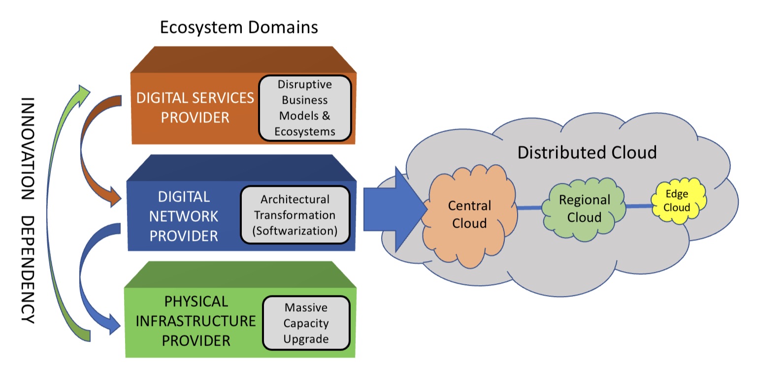
The telecom ecosystem
The TEG segments the telecommunications ecosystem into three domains (see diagram).
The large-scale data centre players are the digital services providers (top layer). In this domain, innovation and competition are greatest.
The digital network provider domain (middle layer) is served by a variety of players, notably the cloud providers, while it is the telcos that dominate the physical infrastructure provider domain.
At this bottom layer, competition is low and overall investment in infrastructure is inadequate. A third of the world’s population still has no access to the internet, notes the report.
The telcos should also be exploiting the synergies between the domains, says the TEG, yet struggle to do so. But more than that, the telcos can be a barrier.
Clarke cites the emerging metaverse that will support immersive virtual worlds as an example.
Metaverse
The “Metaverse” is a concept being promoted by the likes of Meta and Microsoft and has been picked up by the telcos, as evident at this week’s MWC Barcelona 22 show.
Meta’s Mark Zuckerberg recently encouraged his staff to focus on long-term thinking as the company transitions to become a metaverse player. “We should take on the challenges that will be the most impactful, even if the full results won’t be seen for years,” he said.
Telcos should be thinking about how to create a network that enables the metaverse, given the data for rendering metaverse environments will come through the telecom network, says Clarke.

“The real innovation will come when you try and understand the needs of the metaverse in terms of networking, and then you get into the telco game,” he says.
Any concentration of metaverse users will generate a data demand likely to exhaust the network capacity available.
“Telcos will say, ‘We aren’t upgrading capacity because we are not getting a return,’ and then metaverse innovation will be slowed down,” says Clarke.
He says much of the innovation needed for the metaverse will be in the network and telcos need to understand the opportunities for them. “The key is what role will the telcos have, not in dollars but network capability, then you start to see where the innovation needs to be done.”
The challenge is that the telcos can’t see beyond their immediate operational challenges, says Clarke: “Anything new creates more operational challenges and therefore needs to be rejected because they don’t have the resources to do anything meaningful.”
He stresses he is full of admiration for telcos’ operations staff: “They know their game.” But in an environment where operational challenges are avoided, innovation is less important.
TEG’s action plan
TEG’s report lists direct actions telcos can take regarding innovation. These cover funding, innovation processes, procurement and increasing competition.
Many of the proposals are designed to help smaller vendors overcome the challenges they face in telecoms. TEG views small vendors and start-ups as vital for the industry to increase competition and innovation.
Under the funding category, TEG wants telcos to allocate a least 5 per cent of procurement to start-ups and small vendors. The group also calls for investment funds to be set up that back infrastructure and middleware vendors, not just over-the-top start-ups.
For innovation, it wants greater disaggregation so as to steer away from monolithic solutions. The group also wants commitments to fast lab-to-field trials (a year) and shorter deployment cycles (two years maximum) of new technologies.
Competition will require a rethink regarding small vendors. At present, all the advantages are with the large vendors. It lists six measures how telcos can help small vendors win business, one being to stop forcing them to partner with large vendors. The TEG wants telcos to ensure enough personnel that small vendors get all the “airtime” they need with the telcos.
Lastly, concerning procurement, telcos can do much more.
One suggestion is to stop sending small vendors large, complex request for proposals (RFPs) that they must respond to in short timescales; small vendors can’t compete with the large RFP teams available to the large vendors.
Also, telcos should stop their harsh negotiating terms such as a 30 per cent additional discount. Such demands can hobble a small vendor.
Innovation
“Innovation comes from left field and if you try to direct it with a telco mindset, you miss it,” says Clarke. “Telcos think they know what ‘good’ looks like when it comes to innovation, but they don’t because they come at it from a monoculture mindset.”
He said that in the TEG discussions, the idea of incubators for start-ups was mentioned. “We have all done incubators,” he says. But success has been limited for the reasons cited above.
He also laments the lack of visionaries in the telecom industry.
A monoculture organisation rejects such individuals. “Telcos don’t like visionaries because culturally they are annoying and they make their life harder,” he says. “Disruptors have left the industry.”
Prospects
The authors are realistic.
Even if their report is taken seriously, they note any change will take time. They also do not expect the industry to be able to effect change without help. The TEG wants government and regulator involvement if the long-term prospects of a crucial industry are to be ensured.
The key is to create an environment that nurtures innovation and here telcos could work collectively to make that happen.
“No telco has it all, but individual ones have strengths,” says Clarke. “If you could somehow combine the strengths of the particular telcos and create such an environment, things will emerge.”
The trick is diversity – get people from different domains together to make judgements as to what promising innovation looks like.
“Bring together the best people and marvelous things happen when you give them a few beers and tell them to solve a problem impacting all of them,” says Clarke. “How can we make that happen?”

The various paths to co-packaged optics

Near package optics has emerged as companies have encountered the complexities of co-packaged optics. It should not be viewed as an alternative to co-packaged optics but rather a pragmatic approach for its implementation.
Co-packaged optics will be one of several hot topics at the upcoming OFC show in March.
Placing optics next to silicon is seen as the only way to meet the future input-output (I/O) requirements of ICs such as Ethernet switches and high-end processors.
For now, pluggable optics do the job of routing traffic between Ethernet switch chips in the data centre. The pluggable modules sit on the switch platform’s front panel at the edge of the printed circuit board (PCB) hosting the switch chip.
But with switch silicon capacity doubling every two years, engineers are being challenged to get data into and out of the chip while ensuring power consumption does not rise.
One way to boost I/O and reduce power is to use on-board optics, bringing the optics onto the PCB nearer the switch chip to shorten the electrical traces linking the two.
The Consortium of On-Board Optics (COBO), set up in 2015, has developed specifications to ensure interoperability between on-board optics products from different vendors.
However, the industry has favoured a shorter still link distance, coupling the optics and ASIC in one package. Such co-packaging is tricky which explains why yet another approach has emerged: near package optics.
I/O bottleneck
“Everyone is looking for tighter and tighter integration between a switch ASIC, or ‘XPU’ chip, and the optics,” says Brad Booth, president at COBO and principal engineer, Azure hardware architecture at Microsoft. XPU is the generic term for an IC such as a CPU, a graphics processing unit (GPU) or even a data processing unit (DPU).
What kick-started interest in co-packaged optics was the desire to reduce power consumption and cost, says Booth. These remain important considerations but the biggest concern is getting sufficient bandwidth on and off these chips.
“The volume of high-speed signalling is constrained by the beachfront available to us,” he says.
Booth cites the example of a 16-lane PCI Express bus that requires 64 electrical traces for data alone, not including the power and ground signalling. “I can do that with two fibres,” says Booth.

Near package optics
With co-packaged optics, the switch chip is typically surrounded by 16 optical modules, all placed on an organic substrate (see diagram below).
“Another name for it is a multi-chip module,” says Nhat Nguyen, senior director, solutions architecture at optical I/O specialist, Ayar Labs.
A 25.6-terabit Ethernet switch chip requires 16, 1.6 terabits-per-second (1.6Tbps) optical modules while upcoming 51.2-terabit switch chips will use 3.2Tbps modules.
“The issue is that the multi-chip module can only be so large,” says Nguyen. “It is challenging with today’s technology to surround the 51.2-terabit ASIC with 16 optical modules.”
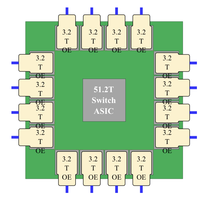
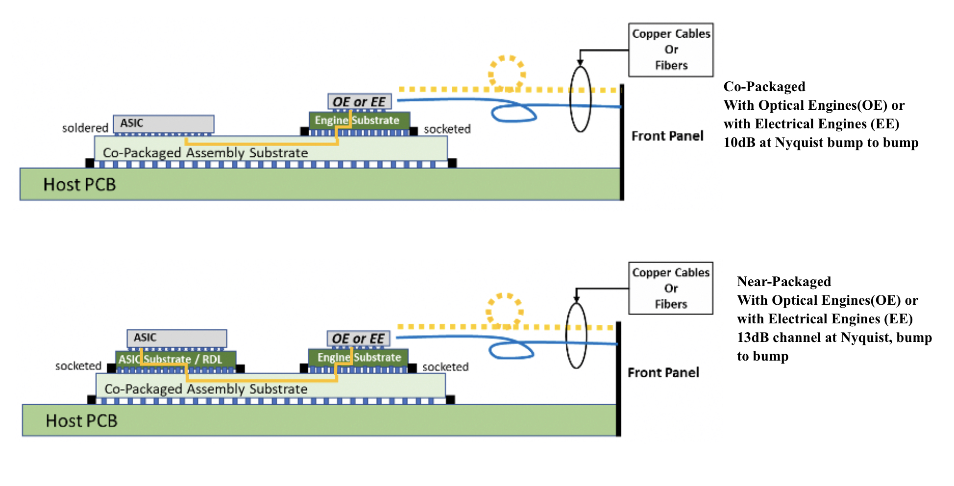
Near package optics tackles this by using a high-performance PCB substrate – an interposer – that sits on the host board, in contrast to co-packaged optics where the modules surround the chip on a multi-chip module substrate.
The near package optics’ interposer is more spacious, making the signal routing between the chip and optical modules easier while still meeting signal integrity requirements. Using the interposer means the whole PCB doesn’t need upgrading which would be extremely costly.
Some co-packaged optics design will use components from multiple suppliers. One concern is how to service a failed optical engine when testing the design before deployment. “That is one reason why a connector-based solution is being proposed,” says Booth. “And that also impacts the size of the substrate.”
A larger substrate is also needed to support both electrical and optical interfaces from the switch chip.
Platforms will not become all-optical immediately and direct-attached copper cabling will continue to be used in the data centre. However, the issue with electrical signalling, as mentioned, is it needs more space than fibre.
“We are in a transitional phase: we are not 100 per cent optics, we are not 100 per cent electrical anymore,” says Booth. “How do you make that transition and still build these systems?”
Perspectives
Ayar Labs views near package optics as akin to COBO. “It’s an attempt to bring COBO much closer to the ASIC,” says Hugo Saleh, senior vice president of commercial operations and managing director of Ayar Labs U.K.
However, COBO’s president, Booth, stresses that near package optics is different from COBO’s on-board optics work.
“The big difference is that COBO uses a PCB motherboard to do the connection whereas near package optics uses a substrate,” he says. “It is closer than where COBO can go.”
It means that with near package optics, there is no high-speed data bandwidth going through the PCB.
Booth says near package optics came about once it became obvious that the latest 51.2-terabit designs – the silicon, optics and the interfaces between them – cannot fit on even the largest organic substrates.
“It was beyond the current manufacturing capabilities,” says Booth. “That was the feedback that came back to Microsoft and Facebook (Meta) as part of our Joint Development Foundation.”
Near package optics is thus a pragmatic solution to an engineering challenge, says Booth. The larger substrate remains a form of co-packaging but it has been given a distinct name to highlight that it is different to the early-version approach.
Nathan Tracy, TE Connectivity and the OIF’s vice president of marketing, admits he is frustrated that the industry is using two terms since co-packaged optics and near package optics achieve the same thing. “It’s just a slight difference in implementation,” says Tracy.
The OIF is an industry forum studying the applications and technology issues of co-packaging and this month published its framework Implementation Agreement (IA) document.
COBO is another organisation working on specifications for co-packaged optics, focussing on connectivity issues.
Technical differences
Ayar Labs highlights the power penalty using near package optics due to its use of longer channel lengths.
For near package optics, lengths between the ASIC and optics can be up to 150mm with the channel loss constrained to 13dB. This is why the OIF is developing the XSR+ electrical interface, to expand the XSR’s reach for near package optics.
In contrast, co-packaged optics confines the modules and host ASIC to 50mm of each other. “The channel loss here is limited to 10dB,” says Nguyen. Co-packaged optics has a lower power consumption because of the shorter spans and 3dB saving.
Ayar Labs highlights its optical engine technology, the TeraPHY chiplet that combines silicon photonics and electronics in one die. The optical module surrounding the ASIC in a co-packaged design typically comprises three chips: the DSP, electrical interface and photonics.
“We can place the chiplet very close to the ASIC,” says Nguyen. The distance between the ASIC and the chiplet can be as close as 3-5mm. Whether on the same interposer Ayar Labs refers to such a design using athird term: in-package optics.
Ayar Labs says its chiplet can also be used for optical modules as part of a co-packaged design.
The very short distances using the chiplet result in a power efficiency of 5pJ/bit whereas that of an optical module is 15pJ/bit. Using TeraPHY for an optical module co-packaged design, the power efficiency is some 7.5pJ/bit, half that of a 3-chip module.
A 3-5mm distance also reduces the latency while the bandwidth density of the chiplet, measured in Gigabit/s/mm, is higher than the optical module.
Co-existence
Booth refers to near package optics as ‘CPO Gen-1’, the first generation of co-packaged optics.
“In essence, you have got to use technologies you have in hand to be able to build something,” says Booth. “Especially in the timeline that we want to demonstrate the technology.”
Is Microsoft backing near package optics?

“We are definitely saying yes if this is what it takes to get the first level of specifications developed,” says Booth.
But that does not mean the first products will be exclusively near package optics.
“Both will be available and around the same time,” says Booth. “There will be near packaged optics solutions that will be multi-vendor and there will be more vertically-integrated designs; like Broadcom, Intel and others can do.”
From an end-user perspective, a multi-vendor capability is desirable, says Booth.
Ayar Labs’ Saleh sees two developing paths.
The first is optical I/O to connect chips in a mesh or as part of memory semantic designs used for high-performance computing and machine learning. Here, the highest bandwidth and lowest power are key design goals.
Ayar Labs has just announced a strategic partnership with high performance computing leader, HPE, to design future silicon photonics solutions for HPE’s Slingshot interconnect that is used for upcoming Exascale supercomputers and also in the data centre.
The second path concerns Ethernet switch chips and here Saleh expects both solutions to co-exist: near package optics will be an interim solution with co-packaged optics dominating longer term. “This will move more slowly as there needs to be interoperability and a wide set of suppliers,” says Saleh.
Booth expects continual design improvements to co-packaged optics. Further out, 2.5D and 3D chip packaging techniques, where silicon is stacked vertically, to be used as part of co-packaged optics designs, he says.