
Turning to optical I/O to open up computing pinch points

Getting data in and out of chips used for modern computing has become a key challenge for designers.
A chip may talk to a neighbouring device in the same platform or to a chip across the data centre.
The sheer quantity of data and the reaches involved – tens or hundreds of meters – is why the industry is turning to optical for a chip’s input-output (I/O).
It is this technology transition that excites Ayar Labs.
The US start-up showcased its latest TeraPHY optical I/O chiplet operating at 1 terabit-per-second (Tbps) during the OFC virtual conference and exhibition held in June.
Evolutionary and revolutionary change
Ayar Labs says two developments are driving optical I/O.
One is the exponential growth in the capacity of Ethernet switch chips used in the data centre. The emergence of 25.6-terabit and soon 51.2-terabit Ethernet switches continue to drive technologies and standards.
This, says Hugo Saleh, vice president of business development and marketing, and recently appointed as the managing director of Ayar Labs’ new UK subsidiary, is an example of evolutionary change.
But artificial intelligence (AI) and high-performance computing have networking needs independent of the Ethernet specification.
“Ethernet is here to stay,” says Saleh. “But we think there is a new class of communications that is required to drive these advanced applications that need low latency and low power.”
Manufacturing processes
Ayar Labs’ TeraPHY chiplet is manufactured using GlobalFoundries’ 45nm RF Silicon on Insulator (45RFSOI) process. But Ayar Labs is also developing TeraPHY silicon using GlobalFoundries’ emerging 45nm CMOS-silicon photonics CLO process (45CLO).
The 45RFSOI process is being used because Ayar Labs is already supplying TeraPHY devices to customers. “They have been going out quite some time,” says Saleh.
But the start-up’s volume production of its chiplets will use GlobalFoundries’ 45CLO silicon photonics process. Version 1.0 of the process design kit (PDK) is expected in early 2022, leading to qualified TeraPHY parts based on the process.
One notable difference between the two processes is that 45RFSOI uses a vertical grating coupler to connect the fibre to the chiplet which requires active alignment. The 45CLO process uses a v-groove structure such that passive alignment can be used, simplifying and speeding up the fibre attachment.
“With high-volume manufacturing – millions and even tens of millions of parts – things like time-in-factory make a big difference,” says Saleh. Every second spent adds cost such that the faster the processes, the more cost-effective and scalable the manufacturing becomes.
Terabit TeraPHY
The TeraPHY chiplet demonstrated during OFC uses eight optical transceivers. Each transceiver comprises eight wavelength-division multiplexed (WDM) channels, each supporting 16 gigabit-per-second (Gbps) of data. The result is a total optical I/O bandwidth of 1.024Tbps operating in each direction (duplex link).
“The demonstration is at 16Gbps and we are going to be driving up to 25Gbps and 32Gbps next,” says Saleh.
The chiplet’s electrical I/O is slower and wider: 16 interfaces, each with 80, 2Gbps channels implementing Intel’s Advanced Interface Bus (AIB) technology.
Last December, Ayar Labs showcased advanced parts using the CLO process. The design was a direct-drive part – a prototype of a future-generation product, not the one demonstrated for OFC.
“The direct-drive part has a serial analogue interface that could come from the host ASIC directly into the ring resonators and modulate them whereas the part we have today is the productised version of an AIB interface with all the macros and all the bandwidth enabled,” says Saleh.
Ayar Labs also demonstrated its 8-laser light source, dubbed SuperNova, that drives the chiplet’s optics.
The eight distributed feedback (DFB) lasers are mixed using a planar lightwave circuit to produce eight channels, each comprising eight frequencies of light.
Saleh compares the SuperNova to a centralised power supply in a server that power pools of CPUs and memory. “The SuperNova mimics that,” he says. “One SuperNova or a 1 rack-unit box of 16 SuperNovas distributing continuous-wave light just like distributed voltage [in a server].”
The current 64-channel SuperNova powers a single TeraPHY but future versions will be able to supply light to two or more.
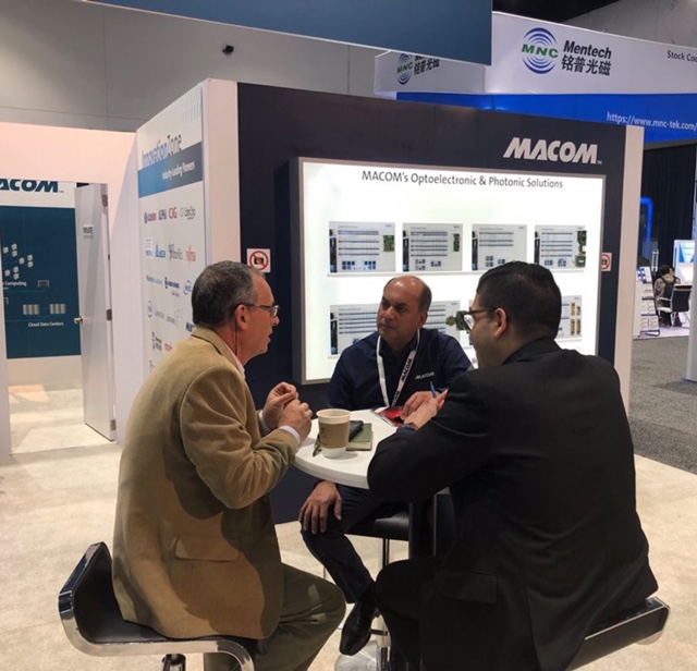
Ayar Labs is using Macom as its volume supplier of DFB lasers.
Significance
Ayar Labs believes the 1-terabit chip-to-chip WDM link is an industry first.
The demo also highlights how the company is getting closer to a design that can be run in the field. The silicon was made less than a month before the demonstration and was assembled quickly. “It was not behind glass and was operating at room temperature,” says Saleh. “It’s not a lab setting but a production setting.”
The same applies to the SuperNova. The light source is compliant with the Continuous-Wave Wavelength Division Multiplexing (CW-WDM) Multi-Source Agreement (MSA) Group that released its first specification revision to coincide with OFC. The CW-WDM MSA Group has developed a specification for 8, 16, and 32-wavelength optical sources.
The CW-WDM MSA promoter and observer members include all the key laser makers as well as the leading ASIC vendors. “We hope to establish an ecosystem on the laser side but also on the optics,” says Saleh.
“Fundamentally, there is a change at the physical (PHY) level that is required to open up these bottlenecks,” says Saleh. “The CW-WDM MSA is key to doing that; without the MSA you will not get that standardisation.”
Saleh also points to the TeraPHY’s optical I/O’s low power consumption which for each link equates to 5pJ/bit. This is about a tenth of the power consumed by electrical I/O especially when retimers are used. Equally, the reach is up to 2km not tens of centimetres associated with electrical links.
Chiplet demand
At OFC, Arista Networks outlined how pluggable optics will be able to address 102.4 terabit Ethernet switches while Microsoft said it expects to deploy co-packaged optics by the second half of 2024.
Nvidia also discussed how it clusters its graphics processing units (GPUs) that are used for AI applications. However, when a GPU from one cluster needs to talk to a GPU in another cluster, a performance hit occurs.
Nvidia is looking for the optical industry to develop interfaces that will enable its GPU systems to scale while appearing as one tightly coupled cluster. This will require low latency links. Instead of microseconds and milliseconds depending on the number of hops, optical I/O reduces the latency to tens of nanoseconds.
“We spec our chiplet as sub-5ns plus the time of flight which is about 5ns per meter,” says Saleh. Accordingly, the transit time between two GPUs 1m apart is 15ns.
Ayar Labs says that after many conversations with switch vendors and cloud players, the consensus is that Ethernet switches will have to adopt co-packaged optics. There will be different introductory points for the technology but the industry direction is clear.
“You are going to see co-packaged optics for Ethernet by 2024 but you should see the first AI fabric system with co-packaged I/O in 2022,” says Saleh.
Intel published a paper at OFC involving its Stratix 10 FPGA using five Ayar Labs’ chiplets, each one operating at 1.6 terabits (each optical channel operating at 25Gbps, not 16Gbps). The resulting FPGA has an optical I/O capacity of 8Tbps, the design part of the US DARPA PIPES (Photonics in the Package for Extreme Scalability) project.
“A key point of the paper is that Intel is yielding functional units,” says Saleh. The paper also highlighted the packaging and assembly achievements and the custom cooling used.
Intel Capital is a strategic investor in Ayar Labs, as is GlobalFoundries, Lockheed Martin Ventures, and Applied Materials.

Macom readies its silicon photonics platform for 400G
-
Macom has announced a laser-integrated photonic integrated circuit (L-PIC) for the 400G-FR4 standard
-
The company is also working with GlobalFoundries to use the semiconductor foundry’s 300mm wafer silicon photonics process
Vivek Rajgarhia (centre) being interviewed at OFC. Source: Macom.
Macom has detailed its latest silicon photonics chip to meet the upcoming demand for 400-gigabit interfaces within the data centre.
The chip, a laser-integrated photonic integrated circuit (L-PIC), was unveiled at the OFC show held last month in San Diego. The L-PIC implements the transmitter circuitry for the 400G FR4 2km interface standard.
Backing silicon photonics
“Five to six years ago, we saw that silicon photonics would have a key role to play in photonics and optical interconnect,” says Vivek Rajgarhia, senior vice president and general manager, lightwave at Macom.
Macom acquired several companies to gain the capabilities needed to become a silicon photonics player.
In 2014 the company paid $230 million for BinOptics which provided Macom with etched facet laser technology that plays a key role in how its L-PIC platform is assembled. Also acquired was the silicon photonics design company, Photonic Controls. In 2015 Macom added FiBest, a packaging specialist, for $60 million.
“We also have the electronics expertise to go alongside [the photonics] to provide chipset solutions,” says Rajgarhia.
>
“Today, as a photonics company, if you don’t have a play in silicon photonics, you are legacy ”
Laser-integrated PIC
The biggest challenge in silicon photonics is integrating the laser, says Rajgarhia. Coupling and aligning the laser, especially when developing optical interfaces for the high-volume data centre market, needs to be done in a cost-effective and scalable way, he says.
The L-PIC, a coarse wavelength division multiplexing (CWDM) design, tackles this by having four cavities for the lasers. “Each laser is flip-chipped and inserted into a cavity without any lens or isolator, and without active alignment,” says Rajgarhia.
The self-alignment is possible by using the etched-facet laser technology from BinOptics. “When you cleave the laser facet, the dimensional control has a lot of play - the tolerance is very high - but with an etched facet, you lithographically define the mechanical dimensions,” he says. “We create a cavity in the silicon that matches the laser’s dimensions.” Macom has also incorporated multiple alignment structures as part of its L-PIC platform to enable the self-alignment.
Macom has already developed the L-PIC for the 100-gigabit CWDM4 standard. “We started with the CWDM4 because it had four wavelengths,” says Rajgarhia. “The CWDM4 is a more challenging design [than the 100-gigabit PSM4 interface] because it requires multiplexing.”
The L-PIC has now been extended to support 100-gigabit channels, to address the DR single channel and the four-channel 400-gigabit FR4 standards. The modulator bandwidth had to be extended and the laser power is different but the approach - the platform - remains the same, says Rajgarhia.
Macom refers to the L-PIC as a smart device. The electro-absorptive modulated lasers (EMLs) used for the FR4 are uncooled. The L-PIC includes ‘structures’ in the silicon such as heaters for tuning the optical elements and photo-detectors that monitor the optical performance. Macom has developed an accompanying micro-controller that sets and controls the device using such structures.
“We have developed software which we give to customers,” says Rajgarhia. “You can type in what extinction ratio you want, what power you want and it sets that up.”
The company has also started the FR4 receiver development that will also be an integrated design with a demultiplexer and four optical receiver channels.
Macom is not saying when the L-PIC will be available. However, the company says 'meaningful demand' for 400-gigabit interfaces will start from 2021.
GlobalFoundries
Macom also announced at OFC that it is working with GlobalFoundries to use the chip maker’s 90nm silicon-on-insulator 300mm wafer processing line.
“Today, as a photonics company, if you don’t have a play in silicon photonics, you are legacy,” says Rajgarhia, adding that in order to make money, what is needed is a working solution that can scale.
“When we started developing [silicon photonics devices], we and others used research foundries to get our products ready,” says Rajgarhia. “Now, what we have announced is that we are scaling this up at GlobalFoundries.”
Macom has started the development at GlobalFoundaries’ East Fishkill fab, the former IBM Microelectronics site that has undertaken a lot of research in silicon photonics, says Rajgarhia.
GlobalFoundries recently created a process development kit (PDK) for its silicon photonics line. Now Macom is an early user of the PDK.
Last year, silicon photonics start-up, Ayar Labs, entered into a strategic agreement with GlobalFoundries, providing the foundry with its optical input-output (I/O) technology while gaining access to its 45nm silicon photonics process.

MACOM acquires Mindspeed to boost 100 Gig offerings
 Ray MoroneyThe Mindspeed acquisition increases the serviceable addressible market for MACOM, both geographical - the company will strengthen its presence in Asia Pacific - and by gaining new equipment vendor accounts. It also broadens MACOM's 100 Gigabit physical device portfolio.
"We are targeting the 100 Gig buildout and the growth coming from that," says Ray Moroney, product line manager, opto-device business unit at MACOM.
Mindpeed also makes a broad portfolio of crosspoint switches used in datacom equipment, and several families of communications processors.
With the acquisition of Mindspeed we have the full electronics bill-of-materials for CFP2 and CFP4 [module] client-side applications
MACOM entered opto-electronics with the acquisition of Optimai in 2011 that had long-haul and client-side modulator drivers and trans-impedance amplifiers (TIAs). Now with Mindspeed's products, MACOM can capture client-side designs with clock data recovery chips and quad-channel TIAs for 100 Gig modules. "With the acquisition of Mindspeed we have the full electronics bill-of-materials for CFP2 and CFP4 [module] client-side applications," says Moroney.
MACOM also gains silicon germanium technology alongside its indium phosphide and gallium arsenide technologies. Silicon germanium has a lower cost structure once a design is being made in volume production, says Moroney, but the R&D and mask costs are generally higher. Silicon germanium also allows significant integration. "It is BiCMOS in nature," says Moroney. "You can integrate full CMOS functionality into a design too." For example digital control can be added alongside analogue functions. Moroney says the company will use silicon germanium for high-performance analogue designs like TIAs as well as high-frequency millimeter wave and microwave applications.
The company is considering its options regarding the future of the communications processors arm of Mindspeed's business. "MACOM is very much an analogue/ RF company," says Moroney. "It [communications processors] is certainly not seen as a core area of investment for MACOM."