ST makes its first PSM4 optical engine deliveries
What gives Benetti confidence is the demand he is seeing for 100-gigabit transceivers in the data centre. “From my visibility today, the tipping point is 2016,” says Benetti, group vice president and general manager, digital and mixed processes ASIC division at STMicroelectronics.
 Flavio Benetti
Benetti and colleagues at ST have spent the last four years working to bring to market the silicon photonics technology that the chip company licensed from Luxtera.
The company has developed a 300mm-wafer silicon photonics production line at its fabrication plant in Crolles that is now up and running. ST also has its first silicon photonics product - a mid-reach PSM4 100-gigabit optical engine - and has just started its very first deliveries.
At the OFC show in March, ST said it had already delivered samples to one unnamed 'customer partner', possibly Luxtera, and Benetti showed a slide of the PSM4 chips as part of a Lumentum transceiver.
Another ST achievement Benetti highlights is the development of a complete supply chain for the technology. In addition to wafer production, ST has developed electro-optic wafer testing. This allows devices to be probed electrically and optically to select working designs before the wafer is diced. ST has also developed a process to 3D-bond chips.
“We have focussed on building an industrial environment, with a supply chain that can deliver hundreds of thousands and millions of devices,” says Benetti.
PSM4 and CWDM4
ST’s first product, the components for a 4x25 gigabit PSM4 transceiver, is a two-chip design.
One chip is the silicon photonics optical engine which integrates the PSM4’s four modulators, four detectors and the grating couplers used to interface the chip to the fibres. The second chip, fabricated using ST’s 55nm BiCMOS process, houses the transceiver’s associated electronics such as the drivers, and trans-impedance amplifiers.
The two chips are combined using 3D packaging. “The 3D packaging consists of the two dies, one copper-pillar bonded to the other,” says Benetti. “It is a dramatic simplification of the mounting process of an optical module.”
The company is also developing a 100-gigabit CWDM4 transceiver which unlike the PSM4 uses four 25-gigabit wavelengths on a single fibre.
The CWDM4 product will be developed using two designs. The first is an interim, hybrid solution that uses an external planar lightwave circuit-based multiplexer and demultiplexer, followed by an integrated silicon photonics design. The hybrid design is being developed and is expected in late 2017; the integrated silicon photonics design is due in 2018.
With the hybrid design, it is not just a question of adding a mux-demux to the PSM4 design. “The four channels are each carrying a different wavelength so there are some changes that need to be done to the PSM4,” says Benetti, adding that ST is working with partners that will provide the mux-demux and do the integration.
We need to have a 100-gigabit solution in high volume for the market, and the pricing pressure that is coming has convinced us that silicon photonics is the right thing to do
Opportunities
Despite the growing demand for 100-gigabit transceivers that ST is seeing, Benetti stresses that these are not 'mobile-phone wafer volumes'. “We are much more limited in terms of wafers,” he says. Accordingly, there is probably only room for one or two large fabs for silicon photonics globally, in his opinion.
So why is ST investing in a large production line? For Benetti, this is an obvious development for the company which has been a provider of electrical ICs for the optical module industry for years.
“ST has entered silicon photonics to provide our customers with a roadmap,” says Benetti. “We need to have a 100-gigabit solution in high volume for the market, and the pricing pressure that is coming has convinced us that silicon photonics is the right thing to do.”
It also offers chip players the possibility of increasing its revenues. “The optical engine integrates all the components that were in the old-fashioned modules so we can increase our revenues there,” he says.
ST is tracking developments for 200-gigabit and 400-gigabit links and is assessing whether there is enough of an opportunity to justify pursuing 200-gigabit interconnects.
For now though, it is seeing strong pricing pressure for 100-gigabit links for reaches of several hundred meters. “We do not think we can compete for very short reach distances,” says Benetti. “We will leave that to VCSELs until the technology can no longer follow.” As link speeds increase, the reach of VCSEL links diminishes. “We will see more room for silicon photonics but this is not the case in the short term,” says Benetti.
Market promise
People have been waiting for years for silicon photonics to become a reality, says Benetti. “My target is to demonstrate it [silicon photonics] is possible, that we are serious in delivering parts to the market in an industrial way and in volumes that have not been delivered before.”
To convince the market, it is not just showing the technological advantages of silicon photonics but the fact that there is a great simplification in constructing the optical module along with the ability to deliver devices in volume. “This is the point,” he says.
Benetti’s other role at ST is overseeing advanced networking ASICs. He argues that over the mid- to long-term, there needs to be a convergence between ASIC and optical connectivity.
“Look at a switch board, for example, you have a big ASIC or two in the middle and a bunch of optical modes on the side,” says Benetti. For him, the two technologies - photonics and ICs - are complementary and the industry’s challenge is to make the two live together in an efficient way.
Silicon photonics: "The excitement has gone"
The opinion of industry analysts regarding silicon photonics is mixed at best. More silicon photonics products are shipping but challenges remain.
Part 1: An analyst perspective
"The excitement has gone,” says Vladimir Kozlov, CEO of LightCounting Market Research. “Now it is the long hard work to deliver products.”
 Dale Murray, LightCounting
However, he is less concerned about recent setbacks and slippages for companies such as Intel that are developing silicon photonics products. This is to be expected, he says, as happens with all emerging technologies.
Mark Lutkowitz, principal at consultancy fibeReality, is more circumspect. “As a general rule, the more that reality sets in, the less impressive silicon photonics gets to be,” he says. “The physics is just hard; light is not naturally inclined to work on the silicon the way electronics does.”
LightCounting, which tracks optical component and modules, says silicon photonics product shipments in volume are happening. The market research firm cites Cisco’s CPAK transceivers, and 40 gigabit PSM4 modules shipping in excess of 100,000 units as examples. Six companies now offer 40 gigabit PSM4 products with Luxtera, a silicon photonics player, having a healthy start on the other five.
Indium phosphide and other technologies will not step back and give silicon photonics a free ride
LightCounting also cites Acacia with its silicon photonics-based low-power 100 and 400 gigabit coherent modules. “At OFC, Acacia made a fairly compelling case, but how much of its modules’ optical performance is down to silicon photonics and how much is down to its advanced coherent DSP chip is unclear,” says Dale Murray, principal analyst at LightCounting. Silicon photonics has not shown itself to be the overwhelming solution for metro/ regional and long-haul networks to date but that could change, he says.
Another trend LightCounting notes is how PAM-4 modulation is becoming adopted within standards. PAM-4 modulates two bits of data per symbol and has been adopted for the emerging 400 Gigabit Ethernet standard. Silicon photonics modulators work really well with PAM-4 and getting it into standards benefits the technology, says LightCounting. “All standards were developed around indium phosphide and gallium arsenide technologies until now,” says Kozlov.
You would be hard pressed to find a lot of OEMs or systems integrators that talk about silicon photonics and what impact it is going to have
Silicon photonics has been tainted due to the amount of hype it has received in recent years, says Murray. Especially the claim that optical products made in a CMOS fabrication plant will be significantly cheaper compared to traditional III-V-based optical components.
First, Murray highlights that no CMOS production line can make photonic devices without adaptation. “And how many wafers starts are there for the whole industry? How much does a [CMOS] wafer cost?” he says.
“You would be hard pressed to find a lot of OEMs or systems integrators that talk about silicon photonics and what impact it is going to have,” says Lutkowitz. “To me, that has always said everything.”
![]() Mark Lutkowitz, fibeReality LightCounting highlights heterogeneous integration as one promising avenue for silicon photonics. Heterogeneous integration involves bonding III-V and silicon wafers before processing the two.
Mark Lutkowitz, fibeReality LightCounting highlights heterogeneous integration as one promising avenue for silicon photonics. Heterogeneous integration involves bonding III-V and silicon wafers before processing the two.
This hybrid approach uses the III-V materials for the active components while benefitting from silicon’s larger (300 mm) wafer sizes and advanced manufacturing techniques.
Such an approach avoids the need to attach and align an external discrete laser. “If that can be integrated into a WDM design, then you have got the potential to realise the dream of silicon photonics,” says Murray. “But it’s not quite there yet.”
This poses a real challenge for silicon photonics: it will only achieve low cost if there are sufficient volumes, but without such volumes it will not achieve a cost differential
Murray says over 30 vendors now make modules at 40 gigabit and above: “There are numerous module types and more are being added all the time.” Then there is silicon photonics which has its own product pie split. This poses a real challenge for silicon photonics: it will only achieve low cost if there are sufficient volumes, but without such volumes it will not achieve a cost differential.
“Indium phosphide and other technologies will not step back and give silicon photonics a free ride, and are going to fight it,” says Kozlov. Nor is it just VCSELs that are made in high volumes.
LightCounting expects over 100 million indium phosphide transceivers to ship this year. Many of these transceivers use distributed feedback (DFB) lasers and many are at 10 gigabit and are inexpensive, says Kozlov.
For FTTx and GPON, bi-directional optical subassemblies (BOSAs) now cost $9, he says: “How much lower cost can you get?”
First silicon photonics devices from STMicro in 2014
STMicroelectronics expects to have first silicon photonics products by mid-2014. The chip company announced the licensing of silicon photonics technology from Luxtera in March 2012. Since then STMicro has been developing its 300mm (12-inch) CMOS wafer manufacturing line for silicon photonics at its fab at Crolles, France.
 Flavio Benetti, STMicroelectronics
"We think we are the only ones doing the processing in a 12-inch line," says Flavio Benetti, general manager of mixed processes division at STMicroelectronics.
The company has a manufacturing agreement with Luxtera and the two continue to collaborate. "We have all the seeds to have a long-term collaboration," says Benetti.
"We also have the freedom to develop our own products." STMicro has long supplied CMOS and BiCMOS ICs to optical module makers, and will make the ICs and its photonic circuits separately.
The company's interest in silicon photonics is due to the growth in data rates and the need of its customers to have more advanced solutions at 100 Gig and 400 Gig in future.
"It is evident that traditional electronics circuits for that are showing their limits in terms of speed, reach and power consumption," says Benetti. "So we have been doing our due diligence in the market, and silicon photonics is one of the possible solutions."
It is evident that traditional electronics circuits for that are showing their limits in terms of speed, reach and power consumption
The chip company will need to fill its 300mm production line and is eyeing short-reach interconnect used in the data centre. STMicro is open to the idea of offering a foundry service to other companies in future but this is not its current strategy, says Benetti: "A foundry model is not excluded in the long term - business is business - but we are not going to release the technology to the open market as a wafer foundry."
The photonic circuits will be made using a 65nm lithography line, chosen as it offers a good tradeoff between manufacturing cost and device feature precision. Test wafers have already been run through the manufacturing line. "Being the first time we put an optical process in a CMOS line, we are very satisfied with the progress," says Benetti.
One challenge with silicon photonics is the ability to get the light in and out of the circuit. "There you have some elements like the gratings couplers - the shape of the grating couplers and the degree of precision are fundamental for the efficiency of the light coupling," says Benetti. "If you use a 90nm CMOS process, it may cost less but 65nm is a good compromise between cost and technical performance." The resulting photonic device and the electronics IC are bonded in a 3D structure and are interfaced using copper pillars.
A foundry model is not excluded in the long term - business is business - but we are not going to release the technology to the open market as a wafer foundry
Making the electronics and photonic chips separately has performance benefits and is more economical: the dedicated photonic circuit is optimised for photonics and there are fewer masks or extra processing layers compared to making an electro-optic, monolithic chip. The customer also has more freedom in the choice of the companion chip - whether to use a CMOS or BiCMOS process. Also some STMicro customers already have a electronic IC that they can reuse. Lastly, says Benetti, customers can upgrade the electronics IC without touching the photonic circuit.
Benetti is already seeing interest from equipment makers to use such silicon photonics designs directly, bypassing the optical module makers. Will such a development simplify the traditional optical supply chain? "There is truth in that; we see that," says Benetti. But he is wary of predicting disruptive change to the traditional supply chain. "System vendors understand the issue of the supply chain with the added margins [at each production stage] but to simplify that, I'm not so sure it is an easy job," he says.
Benetti also highlights the progress being made with silicon photonics circuit design tools.
STMicro's test circuits currently in the fab have been developed using electronic design automation (EDA) tools. "Already the first generation design kit is rather complete - not only the physical design tools for the optics and electronics but also the ability to simulate the system [the two together] with the EDA tools," says Benetti.
But challenges remain.
One is the ability to get light in and out of the chip in an industrial way. "Coupling the light in the fibre attachment - these are processes that still have a high degree of improvement," says Benetti. "The process of the fibre attachment and the packaging is something we are working a lot on. We have today at a very good stage of speed and precision in the placement of the fibres but there is still much we can do."
Luxtera's interconnect strategy
Part 1: Optical interconnect
Luxtera demonstrated a 100 Gigabit QSFP optical module at the OFC/NFOEC 2013 exhibition.
 "We're in discussions with a lot of memory vendors, switch vendors and different ASIC providers"
Chris Bergey, Luxtera
The silicon photonics-based QSFP pluggable transceiver was part of the Optical Internetworking Forum's (OIF) multi-vendor demonstration of the 4x25 Gigabit chip-to-module interface, defined by the CEI-28G-VSR Implementation Agreement.
The OIF demonstration involved several optical module and chip companies and included CFP2 modules running the 100GBASE-LR4 10km standard alongside Luxtera's 4x28 Gigabit-per-second (Gbps) silicon photonics-based QSFP28.
Kotura also previewed a 100Gbps QSFP at OFC/NFOEC but its silicon photonics design uses two chips and wavelength-division multiplexing (WDM).
The Luxtera QSFP28 is being aimed at data centre applications and has a 500m reach although Luxtera says up to 2km is possible. The QSFP28 is sampling to initial customers and will be in production next year.
100 Gigabit modules
Current 100GBASE-LR4 client-side interfaces are available in the CFP form factor. OFC/NFOEC 2013 saw the announcement of two smaller pluggable form factors at 100Gbps: the CFP2, the next pluggable on the CFP MSA roadmap, and Cisco Systems' in-house CPAK.
Now silicon photonics player Luxtera is coming to market with a QSFP-based 100 Gigabit interface, more compact than the CFP2 and CPAK.
The QSFP is already available as a 40Gbps interface. The 40Gbps QSFP also supports four independent 10Gbps interfaces. The QSFP form factor, along with the SFP+, are widely used on the front panels of data centre switches.
"The QSFP is an inside-the-data-centre connector while the CFP/CFP2 is an edge of the data centre, and for telecom, an edge router connector," says Chris Bergey, vice president of marketing at Luxtera. "These are different markets in terms of their power consumption and cost."
Bergey says the big 'Web 2.0' data centre operators like the reach and density offered by the 100Gbps QSFP as their data centres are physically large and use flatter, less tiered switch architectures.
"If you are a big systems company and you are betting on your flagship chip, you better have multiple sources"
The content service providers also buy transceivers in large volumes and like that the Luxtera QSFP works over single-mode fibre which is cheaper than multi-mode fibre. "All these factors lead to where we think silicon photonics plays in a big way," says Bergey.
The 100Gbps QSFP must deliver a lower cost-per-bit compared to the 40Gbps QSFP if it is to be adopted widely. Luxtera estimates that the QSFP28 will cost less than US $1,000 and could be as low as $250.
Optical interconnect
Luxtera says its focus is on low-cost, high-density interconnect rather than optical transceivers. "We want to be a chip company," says Bergey.
The company defines optical interconnect as covering active optical cable and transceivers, optical engines used as board-mounted optics placed next to chips, and ASICs with optical SerDes (serialiser/ deserialisers) rather than copper ones.
Optical interconnect, it argues, will have a three-stage evolution: starting with face-plate transceivers, moving to mid-board optics and then ASICS with optical interfaces. Such optical interconnect developments promise lower cost high-speed designs and new ways to architect systems.
Currently optics are largely confined to transceivers on a system׳s front panel. The exceptions are high-end supercomputer systems and emerging novel designs such as Compass-EOS's IP core router.
"The problem with the front panel is the density you can achieve is somewhat limited," says Bergey. Leading switch IC suppliers using a 40nm CMOS process are capable of a Terabit of switching. "That matches really well if you put a ton of QSFPs on the front panel," says Bergey.
But once switch IC vendors use the next CMOS process node, the switching capacity will rise to several Terabits. This becomes far more challenging to meet using front panel optics and will be more costly compared to putting board-mounted optics alongside the chip.
"When we build [silicon photonics] chips, we can package them in QSFPs for the front panel, or we can package them for mid-board optics," says Bergey.
"If it [silicon photonics] is viewed as exotic, it is never going to hit the volumes we aspire to."
The use of mid-board optics by system vendors is the second stage in the evolution of optical interconnect. "It [mid-board optics] is an intermediate step between how you move from copper I/O [input/output] to optical I/O," says Bergey.
The use of mid-board optics requires less power, especially when using 25Gbps signals, says Bergey: “You dont need as many [signal] retimers.” It also saves power consumed by the SerDes - from 2W for each SerDes to 1W, since the mid-board optics are closer and signals need not be driven all the way to the front panel. "You are saving 2W per 100 Gig and if you are doing several Terabits, that adds up," says Bergey.
The end game is optical I/O. This will be required wherever there are dense I/O requirements and where a lot of traffic is aggregated.
Luxtera, as a silicon photonics player, is pursuing an approach to integrate optics with VLSI devices. "We're in discussions with a lot of memory vendors, switch vendors and different ASIC providers," says Bergey.
Silicon photonics fab
Last year STMicroelectronics (ST) and Luxtera announced they would create a 300mm wafer silicon photonics process at ST's facility in Crolles, France.
Luxtera expects that line to be qualified, ramped and in production in 2014. Before then, devices need to be built, qualified and tested for their reliability.
"If you are a big systems company and you are betting on your flagship chip, you better have multiple sources," says Bergey. "That is what we are doing with ST: it drastically expands the total available market of silicon photonics and it is something that ST and Luxtera can benefit from.”
Having multiple sources is important, says Bergey: "If it [silicon photonics] is viewed as exotic, it is never going to hit the volumes we aspire to."
Part 2: Bell Labs on silicon photonics click here
Part 3: Is silicon photonics an industry game-changer? click here
Altera unveils its optical FPGA prototype
Altera has been showcasing a field-programmable gate array (FPGA) chip with optical interfaces. The 'optical FPGA' prototype makes use of parallel optical interfaces from Avago Technologies.
Combining the FPGA with optics extends the reach of the chip's transceivers to up to 100m. Such a device, once commercially available, will be used to connect high-speed electronics on a line card without requiring exotic printed circuit board (PCB) materials. An optical FPGA will also be used to link equipment such as Ethernet switches in the data centre.
"It is solving a problem the industry is going to face," says Craig Davis, product marketing manager at Altera. "As you go to faster bit-rate transceivers, the losses on the PCB become huge."
What has been done
Altera's optical FPGA technology demonstrator combines a large FPGA - a Stratix IV EP4S100G5 - to two Avago 'MicroPod' 12x10.3 Gigabit-per-second (Gbps) optical engines.
 Avago's MicroPod 12x10Gbps optical engine deviceThe FPGA used has 28, 11.3Gbps electrical transceivers and in the optical FPGA implementation, 12 of the interfaces connect to the two MicroPods, a transmitter optical sub-assembly (TOSA) and a receiver optical sub-assembly (ROSA).
The MicroPod measures 8x8mm and uses 850nm VCSELs. The two optical engines interface to a MTP connector and consume 2-3W. Each MicroPod sits in a housing - a land grid array compression socket - that is integrated as part of the FPGA package.
"The reason we are doing it [the demonstrator] with a 10 Gig FPGA and 10 Gig transceivers is that they are known, good technologies," says Davis. "It is a production GT part and known Avago optics."
Why it matters
FPGAs, with their huge digital logic resources and multiple high-speed electrical interfaces, are playing an increasingly important role in telecom and datacom equipment as the cost to develop application-specific standard product (ASSP) devices continues to rise.
The 40nm-CMOS Stratix IV FPGA family have up to 32, 11.3Gbps transceivers, while Altera's latest 28nm Stratix V FPGAs support up to 66x14.1Gbps transceivers, or 4x28Gbps and 32x12.5Gbps electrical transceivers on-chip.
Altera's FPGAs can implement the 10GBASE-KR backplane standard at spans of up to 40 inches. "You have got the distances on the line card, the two end connectors and whatever the distances are across a 19-inch rack," says Davis. Moving to 28Gbps transceivers, the distance is reduced significantly to several inches only. To counter such losses expensive PCBs must be used.
One way to solve this problem is to go optical, says Davis. Adding 12-channel 10Gbps optical engines means that the reach of the FPGAs is up to 100m, simplifying PCB design and reducing cost while enabling racks and systems to be linked.
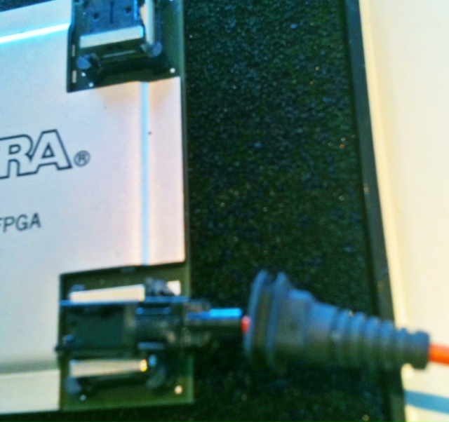 The multimode fibre connector to the MicroPod
Developing an optical FPGA prototype highlights that chip vendors already recognise the role optical interfaces will play.
It is also good news for optical component players as the chip market promises a future with orders of magnitude greater volumes than the traditional telecom market.
The optical FPGA is one target market for silicon photonics players. One, Luxtera, has already demonstrated its technology operating at 28Gbps.
What next
Altera stresses that this is a technology demonstrator only.
The company has not made any announcements regarding when its first optical FPGA product will be launched, and whether the optical technology will enter the market interfacing to its FPGAs' 11.3Gbps, 14.1Gbps or highest-speed 28Gbps transceivers.
 The undersideof the FPGA, showing the 1,932-pin ball grid array
Luxtera's 100 Gigabit silicon photonics chip
Luxtera has detailed a 4x28 Gigabit optical transceiver chip. The silicon photonics company is aiming the device at embedded applications such as system backplanes and high-performance computing (HPC). The chip is also being used by Molex for 100 Gigabit active optical cables. Molex bought Luxtera's active optical cable business in January 2011.

“Do I want to invest in a copper backplane for a single generation or do I switch over now to optics and have a future-proof three-generation chassis?”
Marek Tlalka, Luxtera
What has been done
To make the optical transceiver, a distributed-feedback (DFB) laser operating at 1490nm is coupled to the silicon photonics CMOS-based chip. One laser only is required to serve the four individually modulated 28Gbps transmit channels, giving the chip a 112Gbps maximum data rate. There are also four receive channels, each using a germanium-based photo-detector that is grown on-chip.
The DFB is the same laser that Luxtera uses for its 4x10Gbps and 4x14Gbps designs. What has been changed is the Mach-Zehnder waveguide-based modulators that must now operate at 28Gbps, and the electronics amplifiers at the receivers. “The chip [at 5mmx6mm] is pretty much the same size as our 4x10 and 4x14 Gig designs,” says Marek Tlalka, director of marketing at Luxtera.
 Source: Luxtera
Luxtera is announcing the 100 Gigabit chip which it is sampling to customers. Molex, for example, will package the chip and the laser to make its active optical cable products. Luxtera will package the transceiver chip and laser in a housing as an OptoPHY, a packaged product it already provides at lower speeds. The company will sell the 100Gbps OptoPHY for embedded applications such as system backplanes and HPC.
Applications
The 100GbE transceiver chip is targeted at next-generation backplane applications as well as active optical cables. And it is enterprise vendors that make switches, routers and blade servers that are considering adopting optical backplanes for their next-generation platforms, says Luxtera.
According to Tlalka, system vendors are moving their backplanes from 15Gbps to 28Gbps: “It is pretty obvious that building an electrical backplane at this data rate will be extremely challenging.”
When vendors design a new chassis, they want it to support three generations of line cards. Even if a system vendor develops a 28Gbps copper-based backplane, it will need to go optical when the backplane data rate increases to 40-50Gbps in 2-3 years’ time and 100Gbps when that speed transition occurs. “Do I want to invest in a copper backplane for a single generation or do I switch over now to optics and have a future-proof three-generation chassis?” says Tlalka.
Exascale computers, 1000x more powerful than existing supercomputers planned for the second half of the decade, is another application area. Here there is a need for 25-28Gbps links between chips, says Tlalka.
System platforms and HPC are ideal candidates for the packaged transceiver chip but longer term Luxtera is eyeing the move of optics inside chips such as ASICs. Such system-on-chip optical integration could include Ethernet switch ICs (See example switch ICs from Broadcom and Intel (Fulcrum)) and network interface cards. Another example highlighted by Tlalka is CPU-memory interfaces.
However such applications are at least five years away and there are significant hurdles to be overcome. These include resolving the business model of such designs as well as the technical challenges of coupling the ASIC to the optics and the associated mechanical design.
Standards
Luxtera's 100Gbps transceiver chip supports a variety of standards.
Operating at 25Gbps per channel, the chip supports 100GbE and Enhanced Data Rate (EDR) Infiniband. The ability to go to 28Gbps per channel means that the transceiver can also support the OTN (optical transport network) standard as well as proprietary backplane protocols that add overhead to the basic 25Gbps data rate.
In addition the chip supports the OIF's short reach and very short reach interfaces that define the interface between an ASIC and the optical module.
The chip is also suited for some of the IEEE Next Generation 100Gbps Optical Ethernet Study Group standards now in development. These interfaces will cover a reach of 30m to 2km.
400GbE and HDR Infiniband
Luxtera says that it is working on different channel ’flavours' of 100G. It is also following developments such as Infiniband Hexadecimal Data Rate (HDR) and 400GbE.
HDR will use 40Gbps channels while there is still an industry debate as to whether 400GbE will be implemented using ten channels, each at 40Gbps, or as a 16x25Gbps design.
The InfiniBand roadmap gets redrawn
“We can already demonstrate in silicon a 30Gbps transmitter."
Marek Tlalka, Luxtera
“Our June 2008 roadmap originally projected 4x EDR at less than 80Gbps data rate for 2011,” says Skip Jones, director of technology at QLogic and co-chair of the IBTA’s marketing working group. “The IBTA has increased the data speeds for 2011 due to demand for higher throughput.” A 26Gbps channel rate - or 104Gbps for 4x EDR - is to accommodate the overhead associated with 64/66bit encoding.
The IBTA has also added an interim speed, dubbed Fourteen Data Rate (FDR), operating at 14Gbps per channel or 56Gbps for 4x FDR. This, says the IBTA, is to address midrange enterprise applications in the data centre. “Many server OEMs’ backplanes can support speeds up to 56Gbps,” says Jones. “For those OEMs doing a server refresh using existing backplanes, 56Gbps will be the solution they’ll be looking to implement.”
The IBTA dismisses claims by some industry voices that the re-jigged roadmap is to stop InfiniBand falling behind 100 Gigabit Ethernet (GbE) while FDR is to advance InfiniBand while laser vendors grapple with the challenge of developing 26Gbps vertical-cavity surface-emitting lasers (VCSELs) for EDR.
Jones points out that 4x Quad Data Rate (QDR) InfiniBand (4x10Gbps) now accounts for between 60 and 70 percent of newly deployed InfiniBand systems, and that 100Gbps EDR will appear in 2011/ 2012. “The IBTA has a good track record of releasing products on time; as such, 100Gbps InfiniBand will come out much faster than 100 Gigabit Ethernet.” FDR, meanwhile, will benefit from 14Gbps VCSELs for Fibre Channel that will be available next year. Jones admits that developing a 26Gbps VCSEL poses a challenge but that “InfiniBand markets are mostly electrical interconnects”.
 “The 4x25G short reach is not going to rise and dominate for quite awhile."
Scott Schube, LightCounting
“VCSELs are going to have a tough time at 26Gbps per lane, though they'll get there,” says Scott Schube, senior analyst and strategist at optical transceiver market research firm, LightCounting. “There's definitely a push to go to 26Gbps per lane to reduce pin counts, and the chip guys look like they will be ready before the VCSELs.”
One company looking to benefit from the emerging market for EDR is Luxtera. The silicon photonics specialist says its modulator has already been demonstrated at 30Gbps. This is fast enough to accommodate EDR, 100 Gigabit Ethernet (a 4-channel design) and the emerging 28Gbps Fibre Channel standard.
“We can already demonstrate in silicon a 30Gbps transmitter using the same laser as in our existing products and modulated in our silicon waveguides,” says Marek Tlalka, vice president of marketing at Luxtera. “That allows us to cover 14Gbps, 26Gbps EDR, parallel Ethernet as well as 28Gbps for serial Fibre Channel.”
Luxtera will need to redesign the transistor circuitry to drive the modulator beyond the current 15Gbps before the design can be brought to market. It will also use an existing silicon modulator design though the company says some optimisation work will be required.
There are two main product offerings from Luxtera: QSFP-based active optical cables and OptoPHY, one and four-channel optical engines. Luxtera’s OptoPHY product is currently being qualified and is not yet in volume production.
For multi-channel designs, Luxtera uses a continuous-wave 1490nm distributed feedback (DFB) laser fed to the modulated channels. Addressing 28Gbps Fibre Channel, an SFP+ form factor will be used. Luxtera may offer a transceiver product or partner with a module maker with Luxtera providing the optical engine. “It’s an open question,” says Tlalka.
 “The IBTA has a good track record of releasing products on time; as such, 100Gbps InfiniBand will come out much faster than 100 Gigabit Ethernet.”
Skip Jones, IBTA
The company has said that the single-channel and four-channel 10Gbps OptoPHY engine consumes 450mW and 800mW respectively. Going to 26Gbps will increase the power consumption but only by several tens of percent, it says.
The first product from Luxtera will be a pluggable cable followed by a companion OptoPHY. The pluggable active optical cable from Luxtera will support 100GbE and EDR Infiniband. “I’d still place my bets on InfiniBand deploying first followed by 100GbE,” says Tlalka.
But Schube warns that Luxtera faces a fundamental challenge “Leading-edge designs based on proprietary technology to solve commodity problems - more bandwidth for out-of-the-box connections - are never going to get widely adopted, though Luxtera can fill a niche for awhile," he says.
There is also much work to be done before 100Gbps interfaces will be deployed. “The 4x25G short reach is not going to rise and dominate for quite awhile, no matter what the component availability is,” says Schube. That is because switch ASICs, backplanes, connectors and line cards will all first need to be redesigned.
Meanwhile the IBTA has also announced two future placeholder data rates on its InfiniBand roadmap: High Data Rate (HDR) due in 2014 and the Next Data Rate (NDR) sometime after. “We will refrain from identifying the exact lane speed until we are closer to that timeframe to avoid confusion and the possibility - and probability - of changing future lane speeds,” says Jones.
And Luxtera says its modulator can go faster still. “I think we can easily go 40 and 50Gbps,” says Tlalka. “After 50Gbps we’ll have to look at new magic.”
UNIC silicon modulator
This is the silicon photonic start-up’s first announced modulator. The design has been developed in conjunction with Sun Microsystems as part of the DAPRA Ultraperformance Nanophotonic Intrachip Communications (UNIC) programme.
 An image of the modulator and a cross-section diagram of the ring waveguide. Source: Kotura
Why is it important?
Optical components use a range of specialist, expensive materials. Silicon is one material that could transform the economics for optics. But for this to happen, the main optical functions – light generation, transmission and detection – need to be supported in silicon. To date, all the required functions except the laser itself - waveguides, modulators and photo-detectors - have been mastered and implemented in silicon.
However, the use of silicon photonics in commercial products has till now been limited. For example, Luxtera makes active optical cable that uses silicon photonics-based transceivers while Kotura has been producing silicon photonics-based VOAs for several years. Its VOA is used within reconfigurable optical add/drop multiplexers (ROADMs) and as a dimmer switch to protect optical receivers from network transients.
Kotura is also supplying its silicon-based Echelle gratings product for 40 and 100 Gigabit Ethernet (GbE) transceiver designs that require the multiplexing and demultiplexing of 4 and 10 wavelengths. The company’s gratings are also being used in Santur’s 100Gbit/s (10x10Gbit/s) transceiver design.
Kotura is in volume production of its VOAs and sampling its Ethernet gratings products, says Arlon Martin, vice-president of marketing and sales at Kotura: “The biggest interest is in 40 Gigabit Ethernet.” Given the small size of the gratings, Kotura is also seeing interest from vendors developing 40GbE transceivers in smaller form factors than the CFP module, such as the QSFP.
This will enable 1Tbit/s data rates over a single fibre to connect high-speed multi-core processor computing elements.
Arlon Martin of Kotura.
But the true potential for silicon photonics, one that promises huge volumes, is very short reach optical interconnects for use in high performance computing and within data centres. Having a low power silicon modulator means it can be integrated with other circuitry in CMOS rather than as a discrete design. Such an integrated approach ensures interconnect reliability.
Method used
There are several ways to modulate a laser. Direct modulation uses electronics to switch the laser on and off at the required rate to imprint the data onto the light. An electro-absorption modulated laser, in contrast, adds an element in front of an always-on laser that either passes or absorbs the light. Kotura’s modulator uses a third approach based on a micro-ring resonator and an adjacent waveguide.
The dimension of the ring – its circumference – dictates when optical resonance occurs. And by carefully matching the power coupling of the micro-ring and waveguide to that of the ring loss, signal attenuation– the light-off condition – is improved. The wavelength at which resonance occurs can be changed by playing with the optical properties of the ring waveguide.
Kotura and Sun have demonstrated the silicon modulator working at up to 11GHz, requiring a peak-to-peak voltage of 2V only. The modulator’s insertion loss is also an attractive 2dB though its working spectrum width is only 0.1nm.
“Our power number – 0.5mW at 10GHz - does not include the driver. But if you want to integrate a number of these on one chip, the low power consumption would enable this,” says Martin. Kotura claims the power consumption achieved is the lowest yet reported.
What next?
The modulator is one of the milestones of the DARPA UNIC programme now into the second of its five-year duration. “This [modulator] is prototype work, not a product,” says Martin, adding that Kotura has not fixed a date as to when the modulator will be commercially used.
As for how the device will ultimately be used, Kotura talks of interfaces operating between 100Gbit/s and 1 Tbit/s. Kotura is already working on an independent programme with CyOptics - the NIST Advanced Technology Programme - developing up to 1Tbit/s links using wavelength division multiplexing (WDM). Such designs use separate laser arrays - each laser at a specific wavelength – as well as gratings and photo-detectors.
In the future inexpensive light sources could generate up to 80 separate modulated lightpaths, Martin says. This will enable 1Tbit/s data rates over a single fibre to connect high-speed multi-core processor computing elements.
Is the idea similar to a broadband light source as proposed for WDM-PON? The UNIC partners have yet to reveal the programme’s detail. “Potentially on the right path,” is all Martin would say.
References:
[1] “Low Vpp, ultralow-energy, compact, high-speed silicon electro-optic modulator.” To read Kotura’s technical paper, click here.
[2] "PHOTONICS APPLIED: INTEGRATED PHOTONICS: Can optical integration solve the computational bottleneck?" OptoIQ, March 1, 2009, click here.
Do multi-source agreements benefit the optical industry?
System vendors may adore optical transceivers but there is a concern about how multi-source agreements originate.
Optical transceiver form factors, defined through multi-source agreements (MSAs), benefit equipment vendors by ensuring there are several suppliers to choose from. No longer must a system vendor develop its own or be locked in with a supplier.
 “Personally, the MSA is the worst thing that has happened to the optical industry”
Marek Tlaka, Luxtera
Pluggables also decouple optics from the line card. A line card can address several applications simply by replacing the module. In contrast, with fixed optics the investment is tied to the line card. A system can also be upgraded by swapping the module with an enhanced specification version once it is available.
But given the variety of modules that datacom and telecom system vendors must support, there are those that argue the MSA process should be streamlined to benefit the industry.
Traditionally, several transceiver vendors collaborate before announcing an MSA. The CFP MSA announced in March 2009, for example, was defined by Finisar, Opnext and Sumitomo Electric Device Innovations. Since then Avago Technologies has become a member.
“The industry has an interesting model,” says Niall Robinson, vice president of product marketing at Mintera. “A couple of companies can get together, work behind closed doors and announce suddenly an MSA and try to make it defacto in the market.”
Robinson contrasts the MSA process with the Optical Interconnecting Forum’s (OIF) 100Gbps line side work that defined guidelines for integrated transmitter and receiver modules. Here service providers and system vendors also contributed. “It was a much more effective and fair process, allowing for industry collaboration,” says Robinson
Matt Traverso, senior manager, technical marketing at Opnext, and involved in the CFP MSA, also favours an open process. “But the view that the way MSAs are run is not open is a bit of a fallacy,” he says.
“Any MSA that is well run requires iteration with suppliers,” says Traverso. The opposite is also true: poorly run MSAs have short lives, he says. Having too open a forum also runs the risk of creating a one-size-fits-all: “One vendor may want to use the MSA as a copper interface while a carrier will want it for long-haul dense WDM.”
Optical transceiver vendors benefit in another way if they are the ones developing MSAs. “Transceiver vendors will not make life tough for themselves,” says Padraig OMathuna, product marketing director at optical device maker, GigOptix. “If MSAs are defined by system vendors, [transceiver] designs would be a lot more challenging.”
Avago Technologies argues for standards bodies to play a role especially as industry resources become more thinly spread.
“MSAs are not standards; there are items left unwritten and not enough double checking is done,” says Sami Nassar, director of marketing, fiber optic products division at Avago Technologies. There are always holes in the specifications, requiring patches and fixes. “If they [transceivers] were driven by standards bodies that would be better,” says Nassar.
Organisations such as the IEEE don’t address packaging and connectors as part of their standards work. But this may have to change. “The real challenge, as the industry thins out, is ensuring the [MSA] work is thorough,” says Dan Rausch, Avago’s senior technical marketing manager, fiber optic products division. “The challenge for the industry going forward is ensuring good engineering and more robust solutions.”
Marek Tlalka, vice president of marketing at Luxtera, goes further, questioning the very merits of the MSA: “Personally, the MSA is the worst thing that has happened to the optical industry.”
Unlike the semiconductor industry where a framer chip once on a line card delivers revenue for years, a transceiver company may design the best product yet six months later be replaced by a cheaper competitor. “The return on investment is lost; all that work for nothing,” says Tlalka.
“Is it a good development or not? MSAs are out there,” says Vladimir Kozlov, CEO of optical transceiver market research firm, LightCounting. “It helps system vendors, giving them a freedom to buy.”
But MSAs have squeezed transceiver makers, says Kozlov, and he worries that it is hindering innovation as companies cut costs to maximize their return on investment.
“There is continual pressure to reduce the price of optics,” adds Daryl Inniss, Ovum’s practice leader components. If operators are to provide video and high definition TV services and grow revenues then bandwidth needs to become dirt cheap. “Even today optics is not cheap,” says Inniss. Certainly MSAs play an important role in reducing costs.
“The transceiver vendors’ challenge is our benefit,” admits Oren Marmur, vice president, optical networking line of business, network solutions division at system vendor, ECI Telecom. “But we have our own challenges at the system level.”
Active optical cable: market drivers
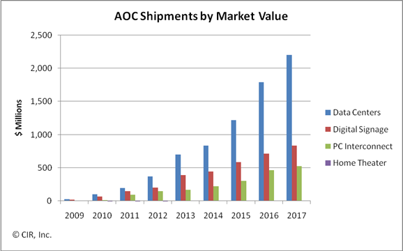
CIR’s report key findings
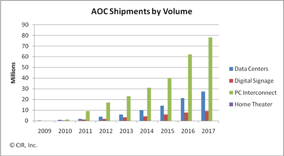
The global market for active optical cable (AOC) is forecast to grow to US $1.5bn by 2014, with the linking of datacenter equipment being the largest single market valued at $835m. Other markets for the cabling technology include digital signage, PC interconnect and home theatre.
CIR’s report entitled Active Optical Cabling: A Technology Assessment and Market Forecast notes how AOC emerged with a jolt. Two years on and the technology is now a permanent fixture that will continue to nimbly address application as they appear. This explains why CIR views AOC as an opportunistic and tactical interconnect technology.

AOC: "Opportunistic and tactical"
Loring Wirbel
What is active optical cable?
An AOC converts an electrical interface to optical for transmission across a cable before being restored to the electrical domain. Optics are embedded as part of the cabling connectors with AOC vendors using proprietary designs. Being self-contained, AOCs have the opportunity to become a retail sale at electronics speciality stores.
A common interface for AOC is the QSFP but there are AOC products that use proprietary interfaces. Indeed the same interface need not be used at each end of the cable. Loring Wirbel, author of the CIR AOC report, mentions a MergeOptics’ design that uses a 12-channel CXP interface at one end and three 4-channel QSFP interfaces at the other. “If it gets traction, everyone will want to do it,” he says.
Origins
AOC products were launched by several vendors in 2007. Start-up Luxtera saw it as an ideal entry market for its silicon photonics technology; Finisar came out with a 10Gbps serial design; while Zarlink identified AOC as a primary market opportunity, says Wirbel.
Application markets
AOC is the latest technology targeting equipment interconnect in the data centre. Typical distances linking equipment range from 10 to 100m; 10m is where 10Gbps copper cabling starts to run out of steam while 100m and above are largely tackled by structured cabling.
“Once you get beyond 100 meters, the only AOC applications I see are outdoor signage and maybe a data centre connecting to satellite operations on a campus,” says Wirbel.
AOC is used to connect servers and storage equipment using either Infiniband or Ethernet. “Keep in mind it is not so much corporate data centres as huge dedicated data centre builds from a Google or a Facebook,” says Wirbel.
AOC’s merits include its extended reach and light weight compared to copper. Servers can require metal plates to support the sheer weight of copper cabling. The technology also competes with optical pluggable transceivers and here the battleground is cost, with active optical cabling including end transceivers and the cable all-in-one.
To date AOC is used for 10Gbps links and for double data rate (DDR) and quad data rate (QDR) Infiniband. But it is the evolution of Infiniband’s roadmap - eight data rate (EDR, 20Gbps per lane) and hexadecimal data rate (HDR, 40Gbps per lane) - as well as the advent of 100m 40 and 100 Gigabit Ethernet links with their four and ten channel designs that will drive AOC demand.
The second largest market for AOC, about $450 million by 2014, and one that surprised Wirbel, is the ‘unassuming’ digital signage.
Until now such signs displaying video have been well served by 1Gbps Ethernet links but now with screens showing live high-definition feeds and four-way split screens 10Gbps feeds are becoming the baseline. Moreover distances of 100m to 1km are common.
PC interconnect is another market where AOC is set to play a role, especially with the inclusion of a high-definition multimedia interface (HDMI) interface as standard with each netbook.
“A netbook has no local storage, using the cloud instead,” says Wirbel. Uploading video from a video camera to the server or connecting video streams to a home screen via HDMI will warrant AOC, says Wirbel.
Home theatre is the fourth emerging application for AOC though Wirbel stresses this will remain a niche application.