
Ciena becomes a computer weaver
- Ciena is to buy optical interconnect start-up Nubis Communications for $270 million.
- The deal covers optical and copper interconnect technology for data centres
Ciena has announced its intention to buy optical engine specialist Nubis Communications for $270 million. If the network is the computer, Nubis’ optical engine and copper integrated circuit (IC) expertise will help Ciena better stitch together AI’s massive compute fabric.
Ciena signalled its intention to target the data centre earlier this year at the OFC show when it showcased its high-speed 448-gigabit serialiser-deserialiser IC technology and coherent lite modem. Now, Ciena has made a move for start-up Nubis, which plays at the core of AI data centres.
“Ciena’s expertise in high-speed components is relevant to 400G per lane Ethernet transceivers, but they never sold any products to this market,” says Vladimir Kozlov, CEO of LightCounting. “Nubis offers them an entry point with several designs and customer engagements.”
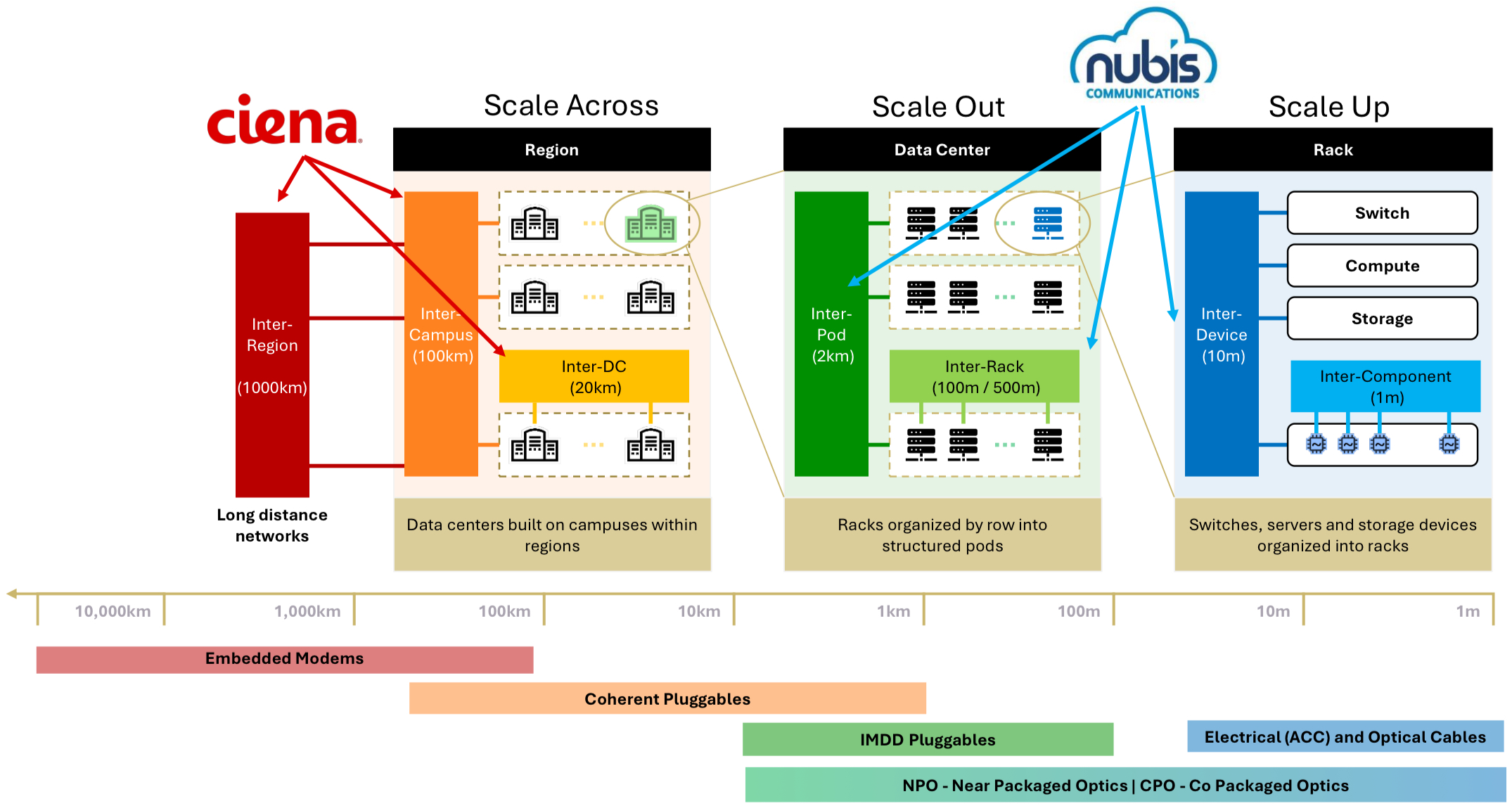
With the deal, Ciena is extending its traditional markets of wide area networks (WAN), metro, and short-reach dense wavelength division multiplexing (DWDM) to include AI networking opportunities. These opportunities include scale-across networks, where AI workloads are shared across multiple data centres, something Ciena can address, to now scale-out and scale-up networks for AI clusters in the data centre.
Puma optical engine
Nubis has developed two generations of compact optical engines for near-package optics (NPO) and co-package optics (CPO) applications. Its first-generation engine operates at 100 gigabits per second (Gbps), while its second, dubbed Puma, operates at 200 Gbps.
Nubis’s optical engine philosophy is based on escaping the optical channels from the surface of the optical engine, not its edge. The start-up also matches the number of optical channels to the electrical ones. The optical engine can be viewed as a sieve: data from the input channels flow through the chip and emerge in the same number of channels at the output. The engine acts as a two-way gateway, with one side handling electrical signals and the other, optical ones.
The Puma optical engine uses 16 channels in each direction, 16 by 200Gbps electrical signals for a total of 3.2 terabits per second (Tbps), and 16 fibres, each fibre carrying 200Gbps of data in the form of a wavelength. Puma’s total capacity is thus 6.4 terabits per second (Tbps). The engine also needs four external lasers to drive the optics, each laser feeding four channels or four fibres. The total fibre bundle of the device consists of 36 fibres: 32 for data (16 for receive and 16 for transmit), and four for the laser light sources.
Nubis is also a proponent of linear drive technology. Here, the advanced serdes on the adjacent semiconductor chip drives the optical engine, thereby avoiding the need for an on-engine digital signal processor (DSP) that requires power. The start-up has also developed a system-based simulator software tool that it uses to model the channel, from the transmitter to the receiver. The tool models not only the electrical and optical components within the channel but also the endpoints, such as the serdes.
Nitro
Nubis has an analogue IC team that designs its trans-impedance amplifiers (TIAs) and drivers used for the optical engine. The hardware compensates for channel impairments with low noise, high linearity, and at high speed. It is this channel simulator tool that Nubis used to optimise its optical engine, and to develop its second key technology, which Nubis calls Nitro —a chip that extends the reach of copper cabling.
“We use our linear optics learning and apply it to copper straight out of the gate, “said Peter Winzer, founder & CTO at Nubis, earlier this year. By using its end-to-end simulator tool, Nubis developed the Nitro IC, which extends the 1m reach of direct-attached copper to 4m using an active copper cable design. “We don’t optimise the driver chip, we optimise the end-to-end system,” says Winzer.
Nubis was also part of a novel design based on a vertical line card to shorten the trace length between an ASIC and pluggable modules.
Ciena’s gain
The acquisition of Nubis places Ciena at the heart of the electrical-optical transition inside the data centre. Ciena will cover both options: copper and optical interconnect. Ciena will gain direct-drive technology expertise for electrical and optical interfaces, enabling scale-up, as well as optical engine technology for scale-out, adding to its coherent technology expertise.

Ciena’s technologies will span coherent ultra-long-haul links all the way to AI accelerators, the heart of AI clusters. By combining Ciena’s 448-gigabit serdes with Nubis’s optical engine expertise, Ciena has a roadmap to develop 12.8Tbps and faster optical engines.
The acquisition places Ciena among new competitors that have chip and optical expertise and deliver co-packaged optics solutions alongside complex ICs such as Broadcom and Marvell.
The deal adds differentiation from Ciena’s traditional system vendor competitors, such as Cisco/ Acacia and Nokia. Huawei is active in long-haul optical and makes AI clusters. Ciena will also compete with existing high-speed optical players, including co-packaged optics specialists Ayar Labs and Ranovus, microLED player Avicena, and optical/IC fabric companies such as LightMatter and Celestial AI.
“Ciena will be a unique supplier in the co-packaged optics/near-packaged optics/active copper cabling data centre interconnect market,” says Daryl Inniss, Omdia’s thought lead of optical components and advanced fibre. “The other suppliers either have multiple products in the intra data centre market, like Broadcom and Nvidia, or they are interconnect-focused start-ups. These suppliers should all wonder what Ciena will do next inside the data centre.”
Ciena will enhance its overall expertise in chips, optics, and signal processing with the Nubis acquisition. It will also put Ciena in front of key processor players and different hyperscaler engineering teams, which drive next-generation AI systems.
Ciena will also have all the necessary parts for the various technologies, regardless of the evolving timescales associated with the copper-to-optical transition within AI systems. Ciena will add direct-detect technology and copper interconnect. On the optical side, it has coherent optical expertise, now coupled with near-package optics and co-packaged optics.
Nubis’ gain
Nubis’ 50-plus staff get a successful exit. The start-up was founded in 2020. Nubis will become a subsidiary of Ciena.
Nubis will be joining a much bigger corporate entity with deep expertise and pockets. Ciena has a good track record with its mergers. Think Nortel at the system level and Blue Planet, a software acquisition. Now the Nubis deal will bring Ciena firmly inside the data centre.
“This is a great deal for Nubis,” says Kozlov. “Congratulations to their team.”
What next?
The deal is expected to close in the fourth quarter of this year. Ciena expects the deal to start adding to its revenues from 2028, requiring Ciena and Nubis to develop products and deliver design wins in the data centre.
“Given the breadth of Ciena’s capabilities, its deep pockets, and products like its data centre out-of-band (DCOM) measurement product, router, and coherent transceivers, one can imagine that Ciena would offer more than co-packaged optics/ near-packaged optics/ active copper cabling inside the data centre,” says Inniss.

Webinar: Scaling AI clusters with optical interconnects
A reminder that this Thursday, September 14th, 8:00-9:00 am PT, I will be taking part in a webcast as part of the OCP Educational Webinar Programme that explores the future of AI computing with optical interconnects.

Data and computation drive AI success, and the hyperscaler are racing to build massive AI accelerator-based compute clusters. The impact of large language models and ChatGPT has turbocharged this race. Scaling demands innovation in accelerator chips, node linkages, fabrics, and topology.
For this webinar, industry experts will discuss the challenge of scaling AI clusters. The other speakers include Cliff Grossner Ph.D., Yang Chen, and Bob Shine. To register, please click here

Books in 2017
Andrew Schmitt, founder and lead analyst of Cignal AI
I didn’t have a good year with books. I bought more than these and either didn’t read them or I lost interest. Hopefully, 2018 will be better.
A Mind at Play: How Claude Shannon Invented the Information Age by Jimmy Soni and Rob Goodman was a big disappointment. It is a well-researched book and has tons of great history on Claude Shannon but there was something about the writing style that made it turgid. I struggled to finish it but learned a lot about Claude Shannon, including that his home in Boston wasn’t far from mine.
The Hard Thing about Hard Things: Building a Business When There are No Easy Answers by Ben Horowitz was the year’s winner. Ben Horowitz started the VC firm A16Z with Marc Andreessen, and both worked at Netscape and later founded Loudcloud. This is easily one of my favourite management books. Each chapter of the book covers an operational topic via a narrative of experiences from the author. Examples include how to build culture and how to scale a sales organisation. The book is highly readable and enjoyable, rare for a title about management advice. Horowitz talks about another book, High Output Management by Andy Grove, which I am reading now.
I reread Cryptonomicon by Neal Stephenson this year for fun. Entertaining book, particularly in light of all the crypto-currency mania. It was written 18 years ago and was way ahead of its time. As William Gibson said, the future is already here, it’s just not evenly distributed. Seveneves was good too (from 2015), but I sure hope that isn’t our future.
The King and Queen of Malibu: The True Story of the Battle for Paradise by David Randall is a history of the large parcel of land now known as Malibu in Southern California. One person owned it after the Spanish American war, and the book is the story of how a rapidly encroaching Los Angeles, spurred on by the automobile, led to its eventual taking by eminent domain. If you know the area and are interested in the history, it is a great book. Otherwise, it is probably of little interest.
I also read a few other sci-fi fiction books while on the road that came highly recommended (Ready Player One, Fortress at the End of Time, Blindsight) but I thought they were not that great.
Vladimir Kozlov, founder and CEO of LightCounting Market Research
I read two books in 2017 that I would highlight.
The first is War and Peace by Leo Tolstoy.
The second is Makers and Takers: The Rise of Finance and the Fall of American Business by Rana Foroohar. The book offers a sobering outlook on modern economic developments and questions the sustainability of growth.
Talking markets: Oclaro on 100 gigabits and beyond
Oclaro’s chief commercial officer, Adam Carter, discusses the 100-gigabit market, optical module trends, silicon photonics, and why this is a good time to be an optical component maker.
Oclaro has started its first quarter 2017 fiscal results as it ended fiscal year 2016 with another record quarter. The company reported revenues of $136 million in the quarter ending in September, 8 percent sequential growth and the company's fifth consecutive quarter of 7 percent or greater revenue growth.
 Adam CarterA large part of Oclaro’s growth was due to strong demand for 100 gigabits across the company’s optical module and component portfolio.
The company has been supplying 100-gigabit client-side optics using the CFP, CFP2 and CFP4 pluggable form factors for a while. “What we saw in June was the first real production ramp of our CFP2-ACO [coherent] module,” says Adam Carter, chief commercial officer at Oclaro. “We have transferred all that manufacturing over to Asia now.”
The CFP2-ACO is being used predominantly for data centre interconnect applications. But Oclaro has also seen first orders from system vendors that are supplying US communications service provider Verizon for its metro buildout.
The company is also seeing strong demand for components from China. “The China market for 100 gigabits has really grown in the last year and we expect it to be pretty stable going forward,” says Carter. LightCounting Market Research in its latest optical market forecast report highlights the importance of China’s 100-gigabit market. China’s massive deployments of FTTx and wireless front haul optics fuelled growth in 2011 to 2015, says LightCounting, but this year it is demand for 100-gigabit dense wavelength-division multiplexing and 100 Gigabit Ethernet optics that is increasing China’s share of the global market.
The China market for 100 gigabits has really grown in the last year and we expect it to be pretty stable going forward
QSFP28 modules
Oclaro is also providing 100-gigabit QSFP28 pluggables for the data centre, in particular, the 100-gigabit PSM4 parallel single-mode module and the 100-gigabit CWDM4 based on wavelength-division multiplexing technology.
2016 was expected to be the year these 100-gigabit optical modules for the data centre would take off. “It has not contributed a huge amount to date but it will start kicking in now,” says Carter. “We always signalled that it would pick up around June.”
One reason why it has taken time for the market for the 100-gigabit QSFP28 modules to take off is the investment needed to ramp manufacturing capacity to meet the demand. “The sheer volume of these modules that will be needed for one of these new big data centres is vast,” says Carter. “Everyone uses similar [manufacturing] equipment and goes to the same suppliers, so bringing in extra capacity has long lead times as well.”
Once a large-scale data centre is fully equipped and powered, it generates instant profit for an Internet content provider. “This is very rapid adoption; the instant monetisation of capital expenditure,” says Carter. “This is a very different scenario from where we were five to ten years ago with the telecom service providers."
Data centre servers and their increasing interface speed to leaf switches are what will drive module rates beyond 100 gigabits, says Carter. Ten Gigabit Ethernet links will be followed by 25 and 50 Gigabit Ethernet. “The lifecycle you have seen at the lower speeds [1 Gigabit and 10 Gigabit] is definitely being shrunk,” says Carter.
Such new speeds will spur 400-gigabit links between the data centre's leaf and spine switches, and between the spine switches. “Two hundred Gigabit Ethernet may be an intermediate step but I’m not sure if that is going to be a big volume or a niche for first movers,” says Carter.
400 gigabit CFP8
Oclaro showed a prototype 400-gigabit module in a CFP8 module at the recent ECOC show in September. The demonstrator is an 8-by-50 gigabit design using 25 gigabaud optics and PAM-4 modulation. The module implements the 400Gbase-LR8 10km standard using eight 1310nm distributed feedback lasers, each with an integrated electro-absorption modulator. The design also uses two 4-wide photo-detector arrays.
“We are using the four lasers we use for the CWDM4 100-gigabit design and we can show we have the other four [wavelength] lasers as well,” says Carter.
Carter says IP core routers will be the main application for the 400Gbase-LR8 module. The company is not yet saying when the 400-gigabit CFP8 module will be generally available.
We can definitely see the CFP2-ACO could support 400 gigabits and above
Coherent
Oclaro is already working with equipment customers to increase the line-side interface density on the front panel of their equipment.
The Optical Internetworking Forum (OIF) has already started work on the CFP8-ACO that will be able to support up to four wavelengths, each supporting up to 400 gigabits. But Carter says Oclaro is working with customers to see how the line-side capacity of the CFP2-ACO can be advanced. “We can definitely see the CFP2-ACO could support 400 gigabits and above,” says Carter. “We are working with customers as to what that looks like and what the schedule will be.”
And there are two other pluggable form factors smaller than the CFP2: the CFP4 and the QSFP28. “Will you get 400 gigabits in a QSFP28? Time will tell, although there is still more work to be done around the technology building blocks,” says Carter.
Vendors are seeking the highest aggregate front panel density, he says: “The higher aggregate bandwidth we are hearing about is 2 terabits but there is a need to potentially going to 3.2 and 4.8 terabits.”
Silicon photonics
Oclaro says it continues to watch closely silicon photonics and to question whether it is a technology that can be brought in-house. But issues remain. “This industry has always used different technologies and everything still needs light to work which means the basic III-V [compound semiconductor] lasers,” says Carter.
“Producing silicon photonics chips versus producing packaged products that meet various industry standards and specifications are still pretty challenging to do in high volume,” says Carter. And integration can be done using either silicon photonics or indium phosphide. “My feeling is that the technologies will co-exist,” says Carter.
Intel's 100-gigabit silicon photonics move
Intel has unveiled two 100-gigabit optical modules for the data centre made using silicon photonics technology.
 Alexis Bjorlin
The PSM4 and CWDM4/CLR4 100-gigabit modules mark the first commercial application of a hybrid integration technique for silicon photonics, dubbed heterogeneous integration, that Intel has been developing for years.
Intel's 100-gigabit module announcement follows the news that Juniper Networks has entered into an agreement to acquire start-up, Aurrion, for $165 million. Aurrion is another silicon photonics player developing this hybrid integration technology for its products.
Hybrid integration
With heterogeneous integration, materials such as indium phosphide and gallium arsenide can be bonded to the silicon substrate before the 300mm wafer is processed to produce the optical circuit. Not only can lasers be added to silicon but other active devices such as modulators and photo-detectors as well as passive functions such as isolators and circulators.
There is no alignment needed; we align the laser with lithography
Intel is using the technique to integrate the laser as part of the 100-gigabit transceiver designs.
"Once we apply the light-emitting material down to the silicon base wafer, we define the laser in silicon," says Alexis Bjorlin, vice president and general manager, Intel Connectivity Group. “There is no alignment needed; we align the laser with lithography.”
Intel claims it gets the highest coupling efficiency between the laser and the optical waveguide and modulator because it is lithographically defined and requires no further alignment.
100-gigabit modules
Intel is already delivering the 100-gigabit PSM4 module. “First volume shipments are happening now,” says Bjorlin. Microsoft is one Internet content provider that is using Intel’s PSM4.
The chip company is also sampling a 100-gigabit CWDM4 module that also meets the more demanding CLR4 Alliance’s optical specification. The 100-gigabit CLR4 module can be used without forward-error correction hardware and is favoured for applications where latency is an issue such as high-performance computing.
Intel is not the first vendor to offer PSM4 modules, nor is it the first to use silicon photonics for such modules. Luxtera and Lumentum are shipping silicon photonics-based PSM4 modules, while STMicroelectronics is already supplying its PSM4 optical engine chip.
We are right on the cusp of the real 100-gigabit connectivity deployments
“Other vendors have been shipping PSM4 modules for years, including large quantities at 40 gigabit,” says Dale Murray, principal analyst at LightCounting Market Research. “Luxtera has the clear lead in silicon photonics-based PSM4 modules but a number of others are shipping them based on conventional optics.”
The PSM4 is implemented using four independent 25-gigabit channels sent over a single-mode ribbon fibre. Four fibres are used for transmission and four fibres for receive.
“The PSM4 configuration is an interesting design that allows one laser to be shared among four separate output fibres,” says Murray. “As Luxtera has shown, it is an effective and efficient way to make use of silicon photonics technology.”
The CWDM4 is also a 4x25-gigabit design but uses wavelength-division multiplexing and hence a single-mode fibre pair. The CWDM4 is a more complex design in that an optical multiplexer and demultiplexer are required and the four lasers operate at different wavelengths.
“While the PSM4 module does not break new ground, Intel’s implementation of WDM via silicon photonics in a CWDM4/CLR4 module could be more interesting in a low-cost QSFP28 module,” says Murray. WDM-based QSFP28 modules are shipping from a number of suppliers that are using conventional optics, he says.
Intel is yet to detail when it will start shipping the CWDM4/CLR4 module.
Market demand
Bjorlin says the PSM4 and the CWDM4/CLR4 will play a role in the data centre. There are applications where being able to break out 100-gigabit into 25-gigabit signals as offered by the PSM4 is useful, while other data centre operators prefer a duplex design due to the efficient use of fibre.
“We are right on the cusp of the real 100-gigabit connectivity deployments,” she says.
As for demand, Bjorlin expects equal demand for the two module types in the early phases: “Longer term, we will probably see more demand for the duplex solution”.
LightCounting says that 100-gigabit PSM4 modules took an early lead in the rollout of 100 Gigabit Ethernet, with VCSEL-based modules not far behind.
“Some are shipping CWDM4/CLR4 and we expect that market to ramp,” says Murray. “Microsoft and Amazon Web Services seem to like PSM4 modules while others want to stick with modules that can use duplex fibre.
 Source: Intel
Data centre switching
“One of the most compelling reasons to drive silicon photonics in the future is that it is an integratable platform,” says Bjorlin.
Switch silicon from the likes of Broadcom support 3.2 terabits of capacity but this will increase to 6.4 terabits by next year and 12.8 terabits using 4-level pulse amplitude modulation (PAM-4) signalling by 2018 (see chart). And by 2020, 25.6-terabit capacity switch chips are expected.
The demand for 100 gigabit is for pluggable modules that fit into the front panels of data center switches. But the market is evolving to 400-gigabit embedded optics that sit on the line card, she says, to enable these emerging higher-capacity switches. Intel is a member of the Consortium of On-Board Optics (COBO) initiative that is being led by Microsoft.
“When you get to 25.6-terabit switches, you start to have a real problem getting the electrical signals in and out of the switch chip,” says Bjorlin. This is where silicon photonics can play a role in the future by co-packaging the optics alongside the switch silicon.
“There will be a need for an integrated solution that affords the best power consumption, the best bandwidth-density that we can get and effectively position silicon photonics for optical I/O [input/output],” says Bjorlin. “Ultimately, that co-packaging is inevitable.”