
OpenLight's CEO on its silicon photonics strategy
Adam Carter, recently appointed the CEO of OpenLight, discusses the company’s strategy and the market opportunities for silicon photonics.
Adam Carter’s path to becoming OpenLight’s first CEO is a circuitous one.
OpenLight, a start-up, offers the marketplace an open silicon photonics platform with integrated lasers and gain blocks.
Having worked at Cisco and Oclaro, which was acquired by Lumentum in 2018, Carter decided to take six months off. Covid then hit, prolonging his time out.
Carter returned as a consultant working with firms, including a venture capitalist (VC). The VC alerted him about OpenLight’s search for a CEO.
Carter’s interest in OpenLight was immediate. He already knew the technology and OpenLight’s engineering team and recognised the platform’s market potential.
“If it works in the way I think it can work, it [the platform] could be very interesting for many companies who don’t have access to the [silicon photonics] technology,” says Carter.
Offerings and strategy
OpenLight’s silicon photonics technology originated at Aurrion, a fabless silicon photonics start-up from the University of California, Santa Barbara.
Aurrion’s heterogeneous integration silicon photonics technology included III-V materials, enabling lasers to be part of the photonic integrated circuit (PIC).
Juniper Networks bought Aurrion in 2016 and, in 2022, spun out the unit that became OpenLight, with Synopsys joining Juniper in backing the start-up.
OpenLight offers companies two services.
The first is design services for firms with no silicon photonics design expertise. OpenLight will develop a silicon photonics chip to meet the company’s specifications and take the design to production.
“If you don’t have a silicon photonics design team, we will do reference architectures for you,” says Carter.
The design is passed to Tower Semiconductor, a silicon photonics foundry that OpenLight, and before that, Juniper, worked with. Chip prototype runs are wafer-level tested and passed to the customer.
OpenLight gives the company the Graphic Data Stream (GDS) file, which defines the mask set the company orders from Tower for the PIC’s production.
OpenLight also serves companies with in-house silicon photonics expertise that until now have not had access to a silicon photonics process with active components: lasers, semiconductor optical amplifiers (SOAs), and modulators.
The components are part of the process design kit (PDK), the set of files that models a foundry’s fabrication process. A company can choose a PDK that best suits its silicon photonics design for the foundry to then make the device.
OpenLight offers two PDKs via Tower Semiconductor: a Synopsys PDK and one from Luceda Photonics.
OpenLight does not make components, but offers reference designs. OpenLight gets a small royalty with every wafer shipped when a company’s design goes to production.
“They [Tower] handle the purchasing orders, the shipments, and if required, they’ll send it to the test house to produce known good die on each wafer,” says Carter
OpenLight plans to expand the foundries it works with. “You have to give customers the maximum choice,” says Carter.
Design focus
OpenLight’s design team continues to add components to its library.
At the OFC show in March, held in San Diego, OpenLight announced a 224-gigabit indium phosphide optical modulator to enable 200-gigabit optical lanes. OpenLight also demoed an eight-by-100-gigabit transmitter alongside Synopsys’s 112-gigabit serialiser-deserialiser (serdes).
OpenLight also offers a ‘PDK sampler’ for firms to gain confidence in its process and designs.
The sampler comes with two PICs. One PIC has every component offered in OpenLight’s PDK so a customer can probe and compare test results with the simulation models of Tower’s PDKs.
”You can get confidence that the process and the design are stable,” says Carter.
The second PIC is the eight by 100 gigabit DR8 design demoed at OFC.
The company is also working on different laser structures to improve the picojoule-per-bit performance of its existing design.
“Three picojoules per bit will be the benchmark, and it will go lower as we understand more about reducing these numbers through design and process,” says Carter.
The company wants to offer the most updated components via its PDK, says Carter.
OpenLight’s small design team can’t do everything at once, he says: “And if I have to license other people’s designs into my PDK, I will, to make sure my customer has a maximum choice.”
Market opportunities
OpenLight’s primary market focus is communications, an established and significant market that will continue to grow in the coming years.
To that can be added artificial intelligence (AI) and machine learning, memory, and high-speed computing, says Carter.
“If you listen to companies like Google, Meta, and Amazon, what they’re saying is that most of their investment in hardware is going into what is needed to support AI and machine learning,” says Carter. “There is a race going on right now.”
When AI and machine learning take off, the volumes of optical connections will grow considerably since the interfaces will not just be for networking but also computing, storage, and memory.
“The industry is not quite ready yet to do that ramp at the bandwidths and the densities needed,” he says, but this will be needed in three to four years.
Large contract manufacturers also see volumes coming and are looking at how to offer optical subassembly, he says.
Another market opportunity is telecoms and, in particular coherent optics for metro networks. However, unit volumes will be critical. “Because I am in a foundry, at scale, I have to fill it with wafers,” says Carter.
Simpler coherent designs – ‘coherent lite’ – connecting data centre buildings could be helpful. There is much interest in short-reach connections, for 10km distances, at 1.6 terabit or higher capacity where coherent could be important and deliver large volumes, he says.
Emerging markets for OpenLight’s platform include lidar, where OpenLight is seeing interest, high-performance computing, and healthcare.
“Lidar is different as it is not standardised,” he says. It is a lucrative market, given how the industry has been funded.
OpenLight wants to offer lidar companies early access to components that they need. Many of these companies have silicon photonics design teams but may not have the actives needed for next-generation products, he says.
“I have a thesis that says everywhere a long-wavelength single-mode laser goes is potential for a PIC,” says Carter
Healthcare opportunities include a monitoring PIC placed on a person’s wrist. Carter also cites machine vision, and cell phone makers who want improved camera depth perception in handsets.
Carter is excited by these emerging silicon photonics markets that promise new incremental revenue streams. But timing will be key.
“We have to get into the right market at the right time with the right product,” says Carter. “If we can do that, then there are opportunities to grow and not rely on one market segment.”
As CEO, how does he view success at OpenLight?
“The employees here, some of whom have been here since the start of Aurrion, have never experienced commercial success,” says Carter. “If that happens, and I think it will because that is why I joined, that would be something I could be proud of.”

Lumentum’s CTO discusses photonic trends
CTO interviews part 2: Brandon Collings
- The importance of moving to parallel channels will only increase given the continual growth in bandwidth.
- Lumentum’s integration of NeoPhotonics’ engineers and products has been completed.
- The use of coherent techniques continues to grow, which is why Lumentum acquired the telecom transmission product lines and staff of IPG Photonics.
“It has changed quite significantly given what Lumentum is engaging in,” he says. “My role spans the entire company; I’m engaged in a lot of areas well beyond communications.”
A decade ago, the main focus was telecom and datacom. Now Lumentum also addresses commercial lasers, 3D sensing, and, increasingly, automotive lidar.
Acquisitions
Lumentum was busy acquiring in 2022. The deal to buy NeoPhotonics closed last August. The month of August was also when Lumentum acquired IPG Photonics’ telecom transmission product lines, including its coherent digital signal processing (DSP) team.
NeoPhotonics’ narrow-linewidth tunable lasers complement Lumentum’s modulators and access tunable modules. Meanwhile, the two companies’ engineering teams and portfolios have now been merged.
NeoPhotonics was active in automotive lidar, but Lumentum stresses it has been tackling the market for several years.
“It’s an area with lots of nuances as to how it is going to be adopted: where, how fast and the cost dependences,” says Collings. “We have been supplying illuminators, VCSELs, narrow-linewidth lasers and other technologies into lidar solutions for several different companies.”
Lumentum gained a series of technological capabilities and some products with the IPG acquisition. “The big part was the DSP capability,” says Collings.
ROADMs
Telecom operators have been assessing IP-over-DWDM anew with the advent of coherent optical modules that plug directly into an IP router.
Cisco’s routed optical networking approach argues the economics of using routers and the IP layer for traffic steering rather than at the optical layer using reconfigurable optical add-drop multiplexers (ROADMs).
Is Lumentum, a leading ROADM technology supplier, seeing such a change?
“I don’t think there is a sea change on the horizon of moving from optical to electrical switching,” says Collings. “The reason is still the same: transceivers are still more expensive than optical switches.”
That balance of when to switch traffic optically or electrically remains at play. Since IP traffic continues to grow, forcing a corresponding increase in signalling speed, savings remain using the optical domain.
“There will, of course, be IP routers in networks but will they take over ROADMs?” says Collings. “It doesn’t seem to be on the horizon because of this growth.”
Meanwhile, the transition to more flexible optical networking using colourless, directionless, contentionless (CDC) ROADMs, is essentially complete.
Lumentum undertook four generations of switch platform design in the last decade to enable CDC-ROADM architectures that are now dominant, says Collings.
Lumentum moved from a simple add-drop to a route-and-select and a colourless, contentionless architecture.
A significant development was Lumentum’s adoption of liquid-crystal-on-silicon (LCOS) technology that enabled twin wavelength-selective switches (WSSes) per node that adds flexibility. LCOS also has enabled a flexible grid which Lumentum knew would be needed.
“We’re increasingly using MEMS technology alongside LCOS to do more complex switching functions embedded in colourless, directionless and contentionless networks today,” says Collings.
Shannon’s limit
If the last decade has been about enabling multiplexing and demultiplexing flexibility, the next challenge will be dealing with Shannon’s limit.
“We can’t stuff much more information into a single optical fibre – or that bit of the amplified spectrum of the optical fibre – and go the same distance,” says Collings. “We’ve sort of tapped out or reached that capacity.”
Adding more capacity requires amplified fibre bandwidth, such as using the L-band alongside the C-band or adding a second fibre.
Enabling such expansion in a cost- and power-efficient way will be fundamental, says Collings, and will define the next generation of optical networks.
Moreover, he expects consumer demand for bandwidth growth to continue. More sensing and more up-hauling of data to the cloud for processing will occur.
Accordingly, optical transceivers will continue to develop over the next decade.
“They are the complement requirement for scaling bandwidth, cost and power effectively,” he says.
Parallelism
Continual growth of bandwidth over the next decade will cause the industry to experience technological ceilings that will drive more parallelism in communications.
“If you look in data centres and datacom interconnects, they have long moved to parallel interface implementations because they felt that bandwidth ceiling from a technological, power dissipation or economic reason.”
Coherent systems have a symbol rate of 128 gigabaud (GBd), and the industry is working on 256GBd systems. Sooner or later, the consensus will be that the symbol rate is fast enough, and it is time to move to a parallel regime.
“In large-scale networks, parallelism is going to be the new thing over the next ten years,” says Collings.
Coherent technology
Collings segments the coherent optical market into three.
There are high-end coherent designs for long-haul transport developed by optical transport vendors such as Ciena, Cisco, Huawei, Infinera and Nokia.
Then there are designs such as 400ZR developed for data centre interconnect. Here a ‘pretty aggressive’ capability is needed but not full-scale performance.
At the lower end, there are application areas where direct-detect optics is reaching its limit. For example, inside the data centre, campus networks and access networks. Here the right solution is coherent or a ‘coherent-light’ technology that is a compromise between direct detection and full-scale coherence used for the long haul.
“So there is emerging this wide continuum of applications that need an equal continuum of coherent technology,” says Collings.
Now that Lumentum has a DSP capability with the IPG acquisition, it can engage with those applications that need solutions that use coherent but may not need the highest-end performance.
800 gigabits and 1.6 terabits
There is also an ongoing debate about the role of coherent for 800-gigabit and 1.6-terabit transceivers, and Collings says the issues remain unclear.
There’s a range of application requirements: 500m, 2km, and 10km. A direct-detect design may meet the 500m application but struggle at 2k and break down at 10km. “There’s a grey area, just in this simple example,” he says.
Also, the introduction of coherent should be nuanced; what is not needed is a long-haul 5,000km DSP. It is more a coherent-light solution or a borrowing from coherent technologies, says Collings: “You’re still trying to solve a problem that you can almost do with direct detect but not quite.”
The aim is to use the minimum needed to accomplish the goal because the design must avoid paying the cost and power to implement the full complement coherent long-haul.
“So that’s the other part of the grey area: how much you borrow?” he says. “And how much do you need to borrow if you’re dealing with 10km versus 2km, or 800 gigabits versus 1.6 terabits.”
Data centres are already using parallel solutions, so there is always the option to double a design through parallelism.
“Eight hundred gigabit could be the baseline with twice as many lanes as whatever we’re doing at 400 gigabits,” he says. “There is always this brute force approach that you need to best if you’re going to bring in new technologies.”
Optical interconnect
Another area Lumentum is active is addressing the issues of artificial intelligence machine-learning clusters. The machine-learning architectures used must scale at an unprecedented rate and use parallelism in processors, multiple such processors per cluster, and multiple clusters.
Scaling processors requires the scaling of their interconnect. This is driving a shift from copper to optics due to the bandwidth growth involved and the distances: 100, 200 and 400 gigabits and lengths of 30-50 meters, respectively.
The transition to an integrated optical interconnect capability will include VCSELs, co-packaged optics, and much denser optical connectivity to connect the graphic processing units (GPUs) rather than architectures based on pluggables that the industry is so familiar with, says Collings.
Co-packaged optics address a power dissipation interconnect challenge and will likely first be used for proprietary interconnect in very high density GPU artificial intelligence clusters.
Meanwhile, pluggable optics will continue to be used with Ethernet switches. The technology is mature and addresses the needs for at least two more generations.
“There’s an expectation that it’s not if but when the switchover happens to co-packaged optics and the Ethernet switch,” says Collings.
Material systems
Lumentum has expertise in several material systems, including indium phosphide, silicon photonics and gallium arsenide.
All these materials have strengths and weaknesses, he says.
Indium phosphide has bandwidth advantages and is best for light generation. Silicon is largely athermal, highly parallelisable and scalable. Staff joining from NeoPhotonics and IPG have strengthened Lumentum’s silicon photonics expertise.
“The question isn’t silicon photonics or indium phosphide. It’s how you get the best out of both material systems, sometimes in the same device,” says Collings. “Sticking in one sandbox is not going to be as competitive as being agile and having the ability to bring those sandboxes together.”

OpenLight's integrated-laser silicon photonics platform

- OpenLight is an independent silicon photonics company backed by Synopsys and Juniper Networks
- The company was created by carving out the silicon photonics arm of Juniper
- The establishment of OpenLight and its open platform highlights the growing maturity of silicon photonics as new applications emerge beyond datacom and telecom
OpenLight is coming to market with an open silicon photonics platform that includes integrated lasers and gain blocks.
Juniper has a long relationship with Synopsys, using its electronic-photonic design automation (EPDA) tools.
So when Juniper said it was spinning out its silicon photonics group, Synopsys was keen to partner. The result is OpenLight, of which Synopsys has a 75 per cent stake costing $67.5 million.
Thomas Mader, OpenLight’s chief operating officer and formerly head of Juniper’s silicon photonics unit, says OpenLight is the first company to offer an open platform that includes monolithically integrated lasers, optical amplifiers and modulators.
Juniper Networks and Synopsys
Juniper gained its silicon photonics technology in 2016 when it acquired Aurrion for $165 million.
Aurrion was a fabless silicon photonics start-up from the University of California, Santa Barbara, with a heterogeneous integration silicon photonics process that includes III-V materials, enabling integrated lasers as part of a photonic circuit.
OpenLight is now making this technology available through its partnership with the foundry Tower Semiconductor.
Juniper’s interests are mainly datacom and telecom, but it recognises the emerging opportunities for silicon photonics such as Lidar, optical computing, high-performance computing and optical interconnect.
“With this kind of technology, you want to drive volumes,” says Mader.

Juniper saw spinning out the unit and opening up access to the technology as the best way to drive volumes and reduce costs. The arrangement also benefits Juniper’s own technology needs.
Synopsys, meanwhile, believes it is the right time to back the OpenLight venture.
“We think it [the open platform] is a great opportunity for growth for Synopsys’s EPDA tools,” says John Koeter, senior vice president of marketing and strategy, solutions group at Synopsys.
OpenLight will give Synopsys insight into how the market is evolving and benefit the company’s tools and, eventually, its IP.
Business model
OpenLight is licensing its process design kit (PDK), the files that model Tower’s fabrication process. A company can enter into an agreement with Tower, access the PDK and design its silicon photonics device.
“What we are offering through Tower, and what we spent significant effort developing and showing Tower how to do, is monolithically integrating lasers and optical gain,” says Mader. “Tower is the first time we’re on a volume eight-inch [wafer] process.”
Juniper entered into a partnership with Tower Semiconductor in 2019.
“We are doing the first MPW [multi-project wafer] this summer with Tower on this process,” says Mader.
OpenLight is also providing designs it has developed and validated for several customers. “But we are not selling PICs [photonic integrated circuits]; that is not part of our plan,” says Mader.
OpenLight intends to partner with other foundries to make more widely available integrated-laser designs.

For now, though, OpenLight is focussed on ratifying its roadmap for the next two years.
“We’re going to be busy building out the component library for Tower to keep customers interested because better components make better circuits,” says Daniel Sparacin, vice president of business development and strategy at OpenLight.
OpenLight offers a 100-gigabit modulator and is working on its next-generation 200-gigabit modulator.
“We’re mostly O-band right now, and we have C-band coming up in the roadmap very shortly,” says Sparacin.
Applications
OpenLight has 400 and 800-gigabit optical designs for the data centre to help customers bring to market their PIC developments.
The company is also seeing interest from Lidar customers, particularly those pursuing coherent-based designs.
“The main reason is the integrated laser,” says Mader. “Otherwise, with standard silicon photonics, you have to attach a laser separately, which doesn’t scale well to multiple channels.” That’s because attaching multiple lasers impacts yield.
Lidar also benefits from on-chip optical amplification. “When you have a complex chip, you have a lot of losses,” says Mader.
OpenLight is working with firms pursuing optical computing for machine learning which promises greater power efficiency. “There are several of them coming to us because we can put hundreds or thousands of indium phosphide elements monolithically on a chip,” says Mader.
OpenLight says it has no position regarding co-packaged optics and whether a design uses an external light source or integrated lasers.
It believes co-packaged optics designs will eventually use integrated light sources, but its technology supports both and can even be used to make external light sources.
Overall, OpenLight says it is working with dozens of companies.
Design tools and integration
Synopsys has been an early mover with its integrated optical design automation tools. The tools include:
- OptoCompiler, a photonic IC design environment.
- The OptSim photonic circuit and system simulator.
- The Sentaurus TCAD and RSoft Photonic Device tools for process modelling and device design.
Working closely with OpenLight will benefit Synopsys’s tool environment, says Koeter. Synopsys is adding functionalities and design capabilities to its tools to support the integration of lasers. OpenLight is also providing Synopsys feedback on what will improve the experience of using its design platform.
Synopsys is one of three leading electronic design automation (EDA) tool companies. However, design tools for photonics are a more recent development.
“EDA quite a while ago is where photonic design is now going,” says Mader.
Integration is the underlying trend driving optics.
“We see the scaling already with 400- and 800-gigabit for datacom and some of the other applications; you see the shift to silicon photonics,” says Mader. “The higher the complexity, the more you see it shifting this way because there’s a cost advantage with the integrated laser and optical gain.”
Photonics may not come close to chip designs with billions of transistors. Still, photonic designs that go beyond four-channel design to ones with 32 or 64 channels or optical computing with hundreds or thousands of components are emerging.
“So you see a scaling even though it’s decades behind the electronics field,” says Mader.
With monolithically integrated lasers, yields remain high, whereas scaling a design with discrete components results in unacceptable yields.
“And so we will be able to go where you can’t go otherwise,” says Mader. “It’s not billions, but even dozens [of components] at this point is revolutionary.”
Intel details its 800-gigabit DR8 optical module

The company earmarks 2023 for its first co-packaged optics product
Intel is sampling an 800-gigabit DR8 in an OSFP pluggable optical module, as announced at the recent OFC virtual conference and show.
“It is the first time we have done a pluggable module with 100-gigabit electrical serdes [serialisers/ deserialisers],” says Robert Blum, Intel’s senior director, marketing and new business. “The transition for the industry to 100-gigabit serdes is a big step.”
The 800-gigabit DR8 module has eight electrical 100-gigabit interfaces and eight single-mode 100-gigabit optical channels in each transmission direction.
Intel demonstrated a prototype 12.8-terabit co-packaged optics design
The attraction of the single-module DR8 design, says Blum, is that it effectively comprises two 400-gigabit DR4 modules. “The optical interface allows you the flexibility that you can break it out into 400-gigabit DR4,” says Blum. “You can also do single 100-gigabit breakouts or you can do 800-gigabit-to-800-gigabit traffic.”
Intel expects volume production of the DR8 in early 2022. Developing a DR8 in a QSFP-DD800 form factor will depend on customer demand, says Blum.
Intel will follow the 800-gigabit DR8 module with a dual 400G FR4, expected later in 2022. The company is also developing a 400-gigabit FR4 module that is expected then.
Meanwhile, Intel is ramping its 200-gigabit FR4 and 400-gigabit DR4 modules.
51.2-terabit co-packaged optics
Intel demonstrated a prototype 12.8-terabit co-packaged optics design, where the optics is integrated alongside its Tofino 2 Ethernet switch chip, at last year’s OFC event.
The company says its first co-packaged optics design will be for 51.2-terabit switches and is scheduled in late 2023. “We see smaller-scale deployments at 51.2 terabits,” says Blum.
Moving the industry from pluggable optical modules to co-packaged optics is a big shift, says Intel. The technology brings clear system benefits such as 30 per cent power savings and lower cost but these must be balanced against the established benefits of using pluggable modules and the need to create industry partnerships for the production of co-packaged optics.
The emergence of 800-gigabit client-side pluggable modules such as Intel’s also means a lesser urgency for co-packaged optics. “You have something that works even if it is more expensive,” says Blum.
Thirty-two 800-gigabit modules can serve a 25.6-terabit switch in a one rack unit (1RU) platform.
However, for Intel, the crossover point occurs once 102.4-terabit switch chips and 200-gigabit electrical interfaces emerge.
“We see co-packaged optics as ubiquitous; we think pluggables will no longer make sense at that point,” says Blum.
FPGA-based optical input-output
Intel published a paper at OFC 2021 highlighting its latest work a part of the U.S. DARPA PIPES programme.
The paper describes a co-packaged optics design that adds 8 terabits of optical input-output (I/0) to its Stratix 10 FPGA. The design uses Ayar Labs’ TeraPHY chiplet for the optical I/O.
The concept is to use optical I/O to connect compute nodes – in this case, FPGAs – that may be 10s or 100s of meters apart.
Intel detailed its first Stratix 10 with co-packaged optical I/O two years ago.
The latest multi-chip package also uses a Stratix 10 FPGA with Intel’s Advanced Interface Bus (AIB), a parallel electrical interface technology, as well as the Embedded Multi-die Interconnect Bridge (EMIB) technology which supports the dense I/O needed to interface the FPGA to the TeraPHY chiplet. The latest design integrates five TeraPHYs compared to the original one that used two. Each chiplet offers 1.6 terabits of capacity such that the FPGA-based co-package has 8 terabits of I/O in total.
Optically enabling Ethernet silicon or an FPGA is part of the industry’s vision to bring optics close to the silicon. Other devices include CPUs and GPUs and machine-learning devices used in computing clusters that require high-density interconnect (see diagram below).
“It is happening first with some of the highest bandwidth Ethernet switches but it is needed with other processors as well,” says Blum.
The Intel OFC 2021 paper concludes that co-packaged optics is inevitable.
Milestones, LiDAR and sensing
Intel has shipped a total of over 5 million 100-gigabit optical modules, generating over $1 billion of revenues.
Blum also mentioned Intel’s Mobileye unit which in January announced its LiDAR-on-a-chip design for autonomous vehicles.
“We have more than 6,000 individual components on this LiDAR photonic integrated circuit,” says Blum. The count includes building blocks such as waveguides, taps, and couplers.
“We have this mature [silicon photonics] platform and we are looking at where else it can be applied,” says Blum.
LiDAR is one obvious example: the chip has dozens of coherent receivers on a chip and dozens of semiconductor optical amplifiers that boost the output power into free space. “You really need to integrate the different functionalities for it to make sense,” says Blum.
Intel is also open to partnering with companies developing biosensors for healthcare and for other sensing applications.
Certain sensors use spectroscopy and Intel can provide a multi-wavelength optical source on a chip as well as ring-resonator technology.
“We are not yet at a point where we are a foundry and people can come but we could have a collaboration where they have an idea and we make it for them,” says Blum.

Silicon Photonics spills over into new markets
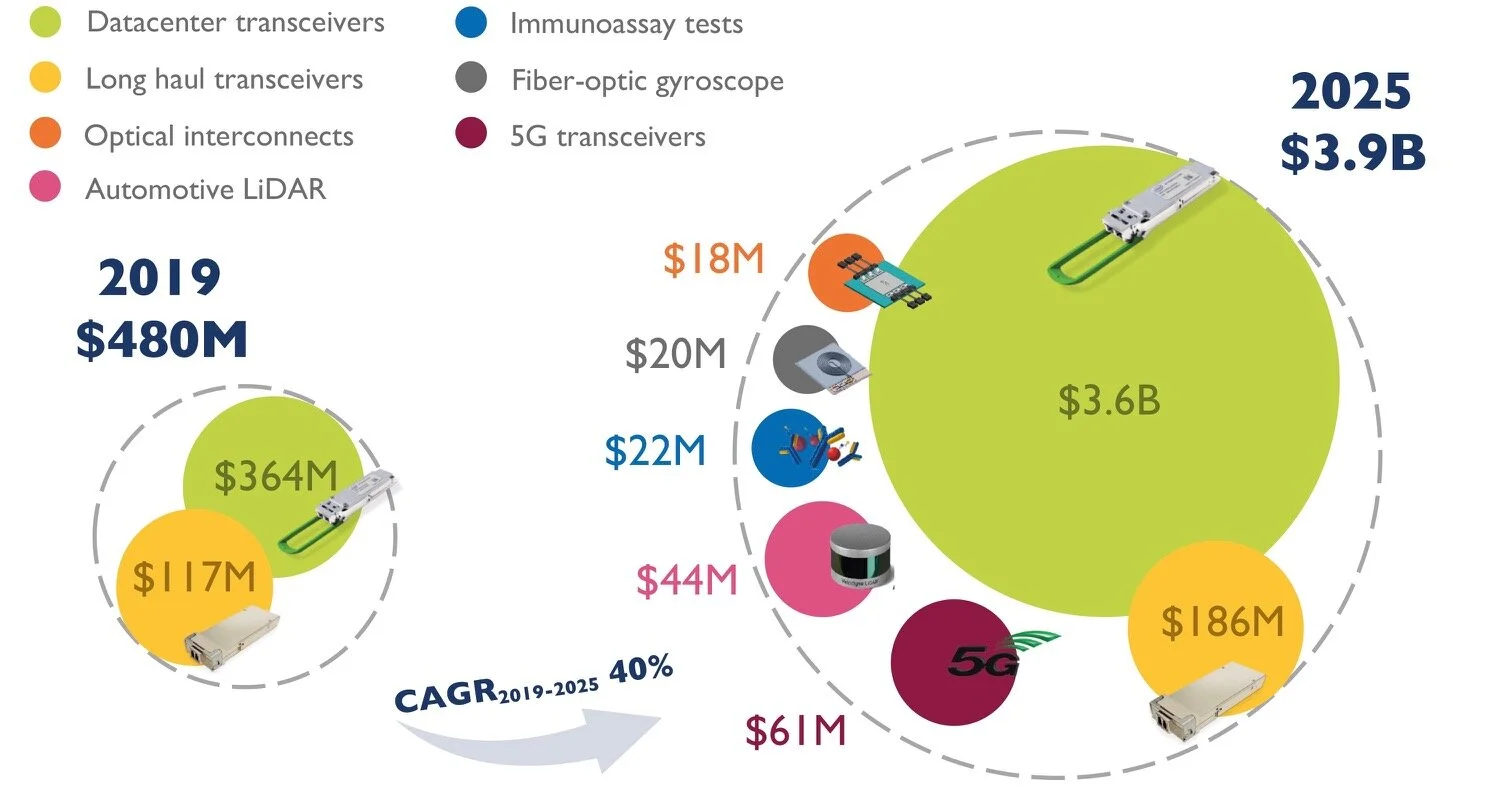
The market for silicon photonics is set to grow eightfold by 2025. So claims market research firm, Yole Développement, in its latest report on silicon photonics, a technology that enables optical components to be made on a silicon substrate.
Silicon photonics is also being used in new markets although optical transceivers will still account for the bulk of the revenues in 2025.
Source: Yole
Market forecast
“We are entering a phase where we are beyond the tipping point [for silicon photonics],” says Eric Mounier, fellow analyst at Yole. “There is no doubt silicon photonics will grow and will be used beyond the data centre.”
Yole sized the 2019 global silicon photonics market at US $480 million, dominated by sales of optical transceivers for the data centre. In 2025 the forecast is for a $3.9 billion market, with data centre transceivers accounting for over 90 per cent of the market.
Eric Mounier
Revenues from new markets such as 5G optical transceivers, automotive, co-packaged optics, fibre-optic gyroscopes, and biochemical sensors will generate $165 million revenues in 2025.
The Yole report also highlights a maturing supply chain, advances in co-packaged optics, and more silicon photonics start-up announcements in the last year.
“It seems the big data centre operators, telecom players and sensor companies are convinced silicon photonics is a key technology for integration, lower cost and smaller components for interconnect and sensing applications,” says Mounier.
Optical transceivers
Data centre optical transceivers account for the bulk of silicon photonics’ market value and unit volumes.
Three-quarters of revenues in 2019 were for data centre transceivers for reaches ranging from several hundred meters to 2km and 10km. This market for silicon photonics is dominated by two players: Intel and Cisco with its Luxtera acquisition.
“For 100-gigabit transceivers, silicon photonics is probably the most used technology compared to legacy optics,” says Mounier.
The remaining 2019 revenues were from long-haul coherent transceiver sales, a market dominated by Acacia that is being acquired by Cisco.
Other companies involved in the transceiver supply chain include Innolight, Juniper Networks, and Alibaba with its work with Elenion Technologies (Elenion was recently acquired by Nokia). HP is working with several firms to develop its silicon photonics supply chain, from device design to final products.
The rollout of 5G is generating a need for 10-gigabit and 25-gigabit transceivers for distances up to 100m, linking remote radio heads and the baseband unit, part of the 5G radio access network.
Yole forecasts a $61 million 5G transceiver market in 2025.
Co-packaged optics
The packaging of optical input-output with a digital chip, known as co-packaged optics, has made notable progress in the last year.
“We are pretty convinced that co-packaged optics is the next big application for silicon photonics,” says Mounier.
Intel has demonstrated its optics packaged with the Tofino 2 Ethernet switch chip it gained with the Barefoot Networks acquisition. “Talking to Intel, I believe in two to three years from now, there will be the first product,” he says.
Other firms pursuing co-packaged optics include Ranovus, Rockley Photonics, Ayar Labs and Sicoya.
The doubling in Ethernet switch-chip capacity every two years is a key driver for co-packaged optics. Switch chips with 25.6-terabit capacity exist and 51.2-terabit switches will be shipping by 2025.
There will also be eight-hundred-gigabit pluggable transceivers in 2025 but Yole says co-packaged optics offers a systems approach to increasing channel counts to keep pace with growing switch capacities.
Foundries and design houses
More than 10 foundries exist worldwide offering silicon photonics services.
“Foundries are interested in silicon photonics because they see a future opportunity for them to fill their fabs,” says Mounier.
Yole cites how GlobalFoundries is working with Ayar Labs, HP with TSMC, Sicoya with IHP Microelectronics, and Rockley Photonics with VTT Memsfab. TSMC also works with Cisco through its Luxtera acquisition.
Swedish MEMS foundry, Silex Microsystems, is developing a portfolio of silicon photonics technology. “They are working with many players developing telecom photonic platforms,” says Mounier.
There are also several design houses offering photonic design services to companies that want to bring products to market. Examples include VLC Photonics, Luceda, Photon Design and Effect Photonics.
Optical design requires know-how that not all firms have, says Mounier. Such silicon photonics design services recall the ASIC design houses that provided a similar service to the electronics industry some two decades ago.
Sensors
Lidar used for autonomous cars and biochemical chips are two emerging sensor markets embracing silicon photonics. Lidar (light detection and ranging) uses light to sense a vehicle’s surroundings.
“Lidar systems are bulky and expensive and a car needs several, at the front, rear and sides,” says Mounier. “Silicon photonics is an emerging platform for the integration of such devices.”
Two Lidar approaches are using silicon photonics: frequency modulation continuous wave (FMCW) Lidar, also known as coherent Lidar, and an optical phased array.
For coherent Lidar, the transmitted frequency of the laser - represented by the local oscillator - and the reflected signal are mixed coherently. This enables phase and amplitude information to be recovered to determine an object’s position and velocity.
SiLC Technologies has developed a FMCW Lidar chip. Working with Varroc Lighting Systems, the two firms have demonstrated Lidar integrated into a car headlamp.
The second approach - an optical phased array - steers the beam of light without using any moving parts.
Lidar is complex and can be implemented using other technologies besides silicon photonics, says Mounier: “Silicon photonics for Lidar has several advantages but it is not clear why the technology will be used in the car or for robotic vehicles.”
In turn, the emerging economic crisis worldwide will likely delay the development of the autonomous car, he says.
Other sensor developments include silicon photonics-based biosensors from Genalyte that use lasers, micro-ring resonators and detectors to produce fast biological test results. The US company has raised over $90 million in three rounds of funding.
French firm Aryballe produces a tiny photonic IC that acts as an electronic nose (digital olfaction). “Using silicon photonics, you can integrate everything on a chip,” says Mounier. “It needs less packaging and assembly and you get a tiny chip at the end.”
COVID-19
Silicon photonics shipments have been delayed in the first half of 2020 due to the COVID-19 pandemic, says Yole. But the market for silicon photonics will still grow this year albeit not at the originally forecasted 10 per cent.
“Everyone is working from home and there is a need for more networking bandwidth,” says Mounier. There will continued demand for transceivers for the data centre and telecom services.
“Market growth will be positive for telecoms, and markets such as defence and medical will not be much impacted,” he says.

Interview: Finisar’s CEO reflects on a notable year
Michael Hurlston has had an eventful 2018.
The year started with him replacing Finisar’s veteran CEO, Jerry Rawls, and it is now ending with Finisar being acquired by the firm II-VI for $3.2 billion.
Finisar is Hurlston’s first experience in the optical component industry, having spent his career in semiconductors. One year in and he already has strong views about the industry and its direction.

Michael Hurlston
“We have seen in the semiconductor industry a period of massive consolidation in the last three to four years,” says Hurlston, in his first interview sinced the deal was announced. “I think it is not that different in optics: scales matters.”
Hurlston says that, right from the start, he recognised the need to drive industry consolidation. “We had started thinking about that fairly deeply at the time the Lumentum-Oclaro acquisition was announced and that gave us more impetus to look at this,” says Hurlston. The result was revealed in November with the announced acquisition of Finisar by II-VI.
“Finisar considered so many deals in the past but could not converge on a solution,” says Vladimir Kozlov, CEO and founder of market research firm, LightCounting. "It needed a new CEO to bring a different perspective. The new II-VI will look more like many diversified semiconductor vendors, addressing multiple markets: automotive, industrial and communications."
“We really have two complementary companies for the most part,” says Hurlston, who highlights VCSELs and reconfigurable optical add-drop multiplexers (ROADMs) as the only product segments where there is overlap. Merging II-VI and Finisar with disparate portfolios further benefits scale, he says.
Chip background
Hurlston’s semiconductor experience was gained at Broadcom and involved Wi-Fi devices. The key lessons he learned there is the importance of offering differentiated products to customers and the need to expand into new application areas.
“Wi-Fi is a standard, a technology, that has rules as you have to interoperate between different chipsets and different producers,” says Hurlston. “But we did find ways to differentiate under a standards umbrella.”
>
“It turns out co-packaging is a great top-line opportunity for optics companies because eventually we will be tasked with pulling together that sub-system”
What he has found, to his surprise, is that it is harder to differentiate in the optical components industry. “What we are trying to do is find spots where we can offer differentiation,” says Hurlston.
Optical components usage needs to also expand into new segments, he says, just as Wi-Fi evolved from a PC-centric technology to home networking and ultimately mobile handsets.
Hurlston cites as an example in the optical components industry how VCSELs are now being used for 3D sensing in handsets. There are also emerging opportunities in automotive and the data centre.
For the automative market, applications include in-cabin sensing to assist drivers and LIDAR (laser detection and ranging) to help vehicles build up an image of their surroundings in real-time. “LIDAR is further out but it is a significant opportunity,” says Hurlston.
For data centres, a key opportunity silicon co-packaging: bringing optics closer to switch silicon.
Currently, switch platform use pluggable optical modules on the faceplate to send and receive data. But with switch silicon capacity doubling every two years, the speed and density of the input-output means optics will have to get closer to the switch silicon.
On-board optics - as promoted by the Consortium for On-Board Optics (COBO) - is one option. Another is co-packaged optics, where the optics and silicon are placed in the same package.
“It turns out co-packaging is a great top-line opportunity for optics companies because eventually we will be tasked with pulling together that sub-system,” says Hurlston. “The integration of the switch chip and optics is something that will be technically difficult and necessitate differentiation.”
Challenges
As well as the issue of acquisitions, another area Hurlston has tackled in his short tenure is Finisar’s manufacturing model and how it can be improved.
“Finisar is a technology company at heart but the life-blood of the company is manufacturing,” he says.
Manufacturing is also one area where there is a notable difference between chips and optics. “There are manufacturing complexities with semiconductors and semiconductor process but optics takes it to a whole different level,” he says.
This is due to the manufacturing complexity of optical transceiver which Finisar’s CEO likens to manufacturing a mobile phone. There are chips that need a printed circuit board onto which are also added optical subassemblies housing such components as lasers and photo-detectors.
“Part of it [the complexity] is the human labour - the human touch - that is involved in the manufacturing and assembling of these transceivers ” he says. Finisar says its laser fab employs several hundred people whereas its optical transceiver factories employ thousands: 5,000 staff in Malaysia and some 5,500 in China.
“Our manufacturing model has been where I’ve spent a lot of time,” says Hurston. Some efficiencies have been gained but not nearly as much as he initially hoped.
Consolidation
One of the issues that has hindered greater industry consolidation has been the need for synergy between companies. A semiconductor company will only acquire or merge with another semiconductor company, and the same with a laser company looking for another laser player, he says. “What I admire about II-VI is that they are pretty bold,” says Hurlston. “What II-VI did is go after something that is not overlapping.”
He believes the creation of such broad-based suppliers is something the optics industry will have to do more of: “The transceiver guys are going to have to go after different areas of the value chain.”
In most mature industries, three large diversified companies typically dominate the marketplace. Given Lumentum’s acquisition of Oclaro has just closed and II-VI’s acquisition of Finisar is due to be completed in mid-2019, will there be another large deal?
“This is a big industry and the opportunity today and going forward is big,” says Hurlston. But there are so many players in different parts of the supply chain such that he is unsure whether these niche companies will survive in the long run.
“Whether there will be three, four or five large players, I don’t know,” he says. “But we are definitely going to see fewer; this [II-VI - Finisar deal] isn't the last transaction that drives industry consolidation.”
>
“Whether there will be three, four or five large players, I don’t know but we are definitely going to see fewer”
How will Finisar make optical transceivers in such a competitive marketplace, that includes an increasing number of Chinese entrants, while delivering gross margins that meet Wall Street expectations?
Finisar does have certain advantages, he says, such as making its own lasers. “We also make our own semiconductors, a lot of the semiconductor solutions the Chinese guys have are sourced,” he says. “That gives us an inherent advantage.”
Having its own manufacturing facilities in the Far East means that Chinese players have no inherent manufacturing advantage there. However, he admits that the gross margin expected of Finisar is higher that its Chinese competitors.
This is why Finisar’s CEO stresses the need to pursue pockets of differentiation and why the company has to be first to market in important productareas that all players will target. “We historically have not been first to market,” he says. “We have made adjustments in the last year in our time-to-market and our ability to get to big products transitions that will be hyper-competitive first.”
Hurston expresses some satisfaction in the improved revenues and gross margins as reported in Finisar’s last two quarters’ results, albeit these quarters coming after what he calls ‘a low base’.
“We have also made significant progress in 3D sensing that has been a big challenge for us,” he says.
What next?
Hurlston says he hopes to have a role in the new company once the deal closes.
“But If I don’t, I’ve really enjoyed working with the [Finisar] team and in this space,” he says. “It’s been a bit of a learning curve but I’ve learnt a couple of tricks. Hopefully there will be another opportunity to apply some of that learning to a job elsewhere.”
Pilot Photonics makes a one terabit coherent comb source
Pilot Photonics has produced a four-wavelength laser chip for one-terabit coherent transmissions.
It is one of several applications the Irish start-up is pursuing using its optical comb source that produces multiple tunable outputs, the equivalent of a laser array.
The company is using its laser technology and photonic integration expertise to address Next Generation Passive Optical Network 2 (NG-PON2), coherent long-haul transmission, and non-telecom applications such as Light Detection and Ranging (LiDAR) and sensing.
 Frank Smyth (right)
“We have a number of chips reaching maturity and we are transitioning from an R&D-focussed company to early commercial activity,” says Frank Smyth, CEO of Pilot Photonics.
Start-up
Pilot Photonics was founded in 2011 and developed a lab instrumentation product. But its limited market resulted in the company changing tack, adding photonic integration expertise to its optical comb source intellectual property.
The company secured two grants that furthered its photonic integration know-how. One - Big Pipes - was a European Commission Seventh Framework Programme (FP7) project addressing optical transport and data centre applications using combs. The second, an Irish government grant, helped the start-up to commercialise its comb technology.
But this was also a challenging period for the company which could only employ two full-time staff. “I wasn't even full time for a few years,” says Smyth, who worked evenings and weekends. “We went into a lean period out of necessity.”
But building a photonic integration capability gained the company a market presence and led to it raising nearly €1million in funding.
Pilot Photonics now has 11 staff and two products being evaluated by customers. One is a directly-modulated laser for NG-PON2 while the second is a fibre-sensing product. The coherent four-channel source chip will soon be its third evaluation product.
The company is also working on a further funding round of several million Euro that it hopes to close by the year-end.
Optical comb source
There are several ways to implement an optical comb source. These include solid-state and fibre-based comb sources commonly used for scientific instrumentation but they are unsuited for high-volume applications, says Smyth.
Pilot Photonics’ approach, dubbed gain switching, is suited to high-volume applications and involves the direct modulation of a laser chip. “A close competitor of our technology is mode-locked laser diodes,” he says. This is the technology used by Ranovus for its module designs.
The start-up claims its technology has distinct advantages. “Our approach gives you better optical properties such as a narrow line-width," he says. The source also offers tunable wavelength spacing, in contrast to most optical combs that use a fixed-cavity design. Pilot Photonics says it can tune the spacing of the sources with sub-kilohertz precision.
The advantage of the comb source for coherent transmission is that a single chip can replace four or eight distinct lasers, saving packaging, size and cost
Pilot Photonics’ comb sources exploit injection locking between two lasers. Injection locking refers to an effect when two closely matched oscillating systems - in this case, lasers - interact to become synchronised.
The start-up’s comb source comprises a short-cavity ‘slave’ laser and a long-cavity ‘master’ one. The slave laser is modulated with a sine wave, turning the laser on briefly each cycle, to create a train of optical light pulses.
Linking the two lasers, injection locking occurs which increases the coherence between the output pulses. As Smyth explains, this reduces the jitter of the slave laser’s output in that the laser is turned on and off at the same exact points each cycle. This turns the slave’s output, when viewed on a spectrum analyser, into equally-spaced narrow line-width light sources.
The dimensions of the master laser’s cavity set the sources’ line widths while their spacing is dictated by the modulating sine wave. The master laser also determines the central wavelength of the comb sources while the sine wave’s frequency sets the spacings either side. “The master laser gives you a locked centre point and then the tones emanating from the centre can be tuned quite precisely,” says Smyth.
Pilot Photonics’ core intellectual property is making the indium-phosphide optical comb source using its patented gain-switching approach.
Photonic integration
The start-up has built a library of indium-phosphide optical functions in addition to the lasers used for the comb source. The functions include semiconductor optical amplifiers, waveguides, optical couplers, splitters and an active optical filter.
The splitters are used to place the comb source output on waveguides while an active optical filter on each selects the wanted source.
“This [active optical filter] is what we use to separate out individual comb lines so we can do fancy things with them,” says Smyth. For example, modulating the source with data, or beating two sources together for frequency multiplication to create sources in the millimetre wave or sub-terahertz ranges.
Pilot Photonics’ optical circuits are built in an indium-phosphide foundry where the comb source fabrication in done without using regrowth stages. This equates to fewer mask stages to process the indium-phosphide wafer. “There is no regrowth of material back over etched areas,” says Smyth. Fewer steps equates to a less-costly manufacturing process and improved yields.
The start-up sees NG-PON2, the 10-gigabit four-wavelength PON standard, as the largest and closest market opportunity for the company. Coherent optical transport is another telecom market the company is pursuing.
“The next closest opportunity is optical fibre sensing,” says Smyth, pointing out that there are several optical fibre sensoring techniques that can be made using their laser as a pulse source.
The company is also developing LiDAR technology and is involved with the European Space Agency to develop a light source for high-frequency metrology applications including atomic clocks and gravity meters.
“It is a very broad range of applications that we can apply the technology to,” says Smyth.
NG-PON2
Pilot Photonics is not using its source technology as a comb for an NG-PON2 optical line terminal (OLT) but rather as a directly modulated laser for the customer premises equipment’ optical network unit (ONU).
“What we have done is develop a wavelength-tunable directly-modulated laser for NG-PON2,” says Smyth. The benefit of its design is that the laser chip meets the stringent specification of the ONU by being tunable, meeting a reach of 40km and enabling sub-$100 designs.
The start-up is engaged with several potential NG-PON2 customers including manufacturers, systems vendors and module makers, and has delivered an evaluation board with the chip to its lead customer.
Two or three network equipment manufacturers are eager to evaluate the chip
Coherent source
The advantage of the comb source for coherent transmission is that a single chip can replace four or eight distinct lasers, saving packaging, size and cost.
Smyth estimates that a four-channel comb source is a third of the cost of a design using four single-mode lasers. The power consumption is also less; only one thermo-electric cooler is required instead of four.
Pilot Photonics says that it has demonstrated its four-channel comb-source transmitting over hundreds of kilometres.
The comb source can be used to send 400-gigabit (100 gigabit/wavelength) and 1-terabit (250 gigabit/wavelength) super-channels. “We’ve done two terabits using 16-QAM on most of the channels and QPSK on the outer ones,” says Smyth.
There are also other system performance benefits using a comb source. There is no need for guard bands to separate between the tones. “You are packing them as tight as can be allowed, the ultimate in spectral efficiency,” he says.
Smyth also points out that non-linear compensation techniques can be used because the frequency spacings are known precisely. Using non-linear compensation methods benefits reach; the laser source can be launched at higher power and the non-linear effects that result can be compensated for.
Pilot Photonics has shown its sources spaced as close as 6.25GHz to 87.5GHz apart. The start-up also says the tones do not need to be evenly spaced.
The start-up now has its four-channel comb-source chip on an evaluation board that it is about to deliver to interested systems vendors and large-scale data centre operators.
“Two or three network equipment manufacturers are eager to evaluate the chip,” says Smyth. “They are less forthcoming as to what they are applying it to.”
IoT will drive chip design and new styles of computing
Looking back 20 years hence, how will this period be viewed? The question was posed by the CEO of imec, Luc Van de hove, during his opening talk at a day event imec organised in Tel-Aviv.
For Van den hove, this period will be seen as one of turbulent technological change. “The world is changing at an incredible rate,” he says. “The era of digital disruption is changing our industry and this disruption is not going to stop.”
 Luc Van den hove
It was the Belgium nonoelectronics R&D centre’s second visit to Israel to promote its chip and systems expertise as it seeks to expand its links with Israel’s high-tech industry. And what most excites imec is the Internet of Things (IoT), the advent of connected smart devices that turn data into information and adapt the environment to our needs.
The world is changing at an incredible rate. The era of digital disruption is changing our industry and this disruption is not going to stop
Internet of Things
Imec is focussing on five IoT areas: Smart Health - wearable and diagnostic devices, Smart Mobility which includes technologies for autonomous cars, drones and robots, Smart Cities, Smart Industry and Smart Energy. “In all these areas we look at how we can leverage our semiconductor know-how,” says Van den hove. “How we can bring innovative solutions by using our microchip technology.”
The broad nature of the IoT means imec must form partnerships across industries while strengthening its systems expertise. In healthcare, for example, imec is working with John Hopkins University, while last October, imec completed the acquisition of iMinds, a Belgium research centre specialising in systems software and security.
“One of the challenges of IoT is that there is not one big killer application,” says Van den hove. “How to bring these technologies to market is a challenge.” And this is where start-ups can play a role and explains why imec is visiting Israel, to build its partnerships with local high-tech firms.
Imec also wants to bring its own technologies to market through start-ups and has established a €100 million investment fund to incubate new ideas and spin-offs.
Technologies
Imec’s expertise ranges from fundamental semiconductor research to complex systems-on-chip. It is focussing on advanced sensor designs for IoT as this is where it feels it can bring an advantage. Imec detailed a radar chip design for cars that operates at 79GHz yet is implemented in CMOS. It is also developing a Light Detection and Ranging (LIDAR) chip for cars based on integrated photonics. Future cars will have between 50 to 100 sensors including cameras, LIDAR, radar and ultrasound.
 Imec's multi-project wafers. Source: imec
The data generated from these sensors must be processed, fused and acted upon. Imec is doing work in the areas of artificial intelligence and machine learning. In particular, it is developing neuromorphic computing devices that use analogue circuits to mimic the biological circuitry of the brain. Quantum computing is another area imec has begun to explore.
One of the challenges of IoT is that there is not one big killer application
“There is going to be so much data generated,” says Van den Hove. “And it is better to do it [processing] locally because computation is cheaper than bandwidth.”
Imec envisages a network with layers of intelligence, from the sensors all the way to the cloud core. As much of the data as possible will be processed by the sensor so that it can pass on more intelligent information to the network edge, also known as fog computing. Meanwhile, the cloud will be used for long-term data storage, for historical trending and for prediction using neuromorphic algorithms, says Van den Hove.
But to perform intensive processing on-chip and send the results off-chip in a power-efficient manner will require advances in semiconductor technology and the continuation of Moore’s law.
Moore's law
Imec remains confident that Moore’s law will continue to advance for some years yet but notes it is getting harder. In the past, semiconductor technology had a predictable roadmap such that chip designers could plan ahead and know their design goals would be met. Now chip technologists and designers must work together, a process dubbed technology-design co-optimisation.
Van den hove cites the example of imec’s work with ARM Holdings to develop a 7nm CMOS process node. “You can create some circuit density improvement just by optimising the design, but you need some specific technology features to do that,” he says. For example, by using a self-alignment technique, fewer metal tracks can be used when designing a chip's standard cell circuitry. "Using the same pitch you get an enormous shrink," he says. But even that is not going to be enough and techniques such as system-technology co-optimisation will be needed.
Imec is working on FinFETs, a style of transistor, to extend CMOS processes down to 5nm and then sees the use of silicon nanowire technology - first horizontal and then vertical designs - to extend the roadmap to 3nm, 2.5nm and even 1.8nm feature sizes.
Imec is also working on 3D chip stacking techniques that will enable multi-layer circuits to be built. “You can use specific technologies for the SRAM, processing cores and the input-output.” Imec is an active silicon photonics player, seeing the technology playing an important role for optical interconnect.
Imec awarded Gordon Moore a lifetime of innovation award last year, and Van den hove spent an afternoon at Moore’s home in Hawaii. Van den hove was struck with Moore’s humility and sharpness: “He was still so interested in the technology and how things were going.”
Mario Paniccia: We are just at the beginning
 During that time, his Intel team had six silicon photonics papers published in the science journals, Nature and Nature Photonics, and held several world records - for the fastest modulator, first at 1 gigabit, then 10 gigabit and finally 40 gigabit, the first pulsed and continuous-wave Raman silicon laser, the first hybrid silicon laser working with The University of California, Santa Barbara, and the fastest silicon germanium photo-detector operating at 40 gigabit.
It got to the stage where Intel’s press relations department would come and ask what the team would be announcing in the coming months. “ 'Hey guys,' I said, 'it doesn't work that way ' ”.
Since leaving Intel last year, Paniccia has been working as a consultant and strategic advisor. He is now exploring opportunities for silicon photonics but in segments other than telecom and datacom.
“I didn't want to go into developing transceivers for other big companies and compete with my team's decade-plus of development; I spent 20 years at Intel,” he says.
Decade of development
Intel’s silicon photonics work originated in the testing of its microprocessors using a technique known as laser voltage probing. Infra-red light is applied to the back side of the silicon to make real-time measurements of the chip’s switching transistors.
For Paniccia, it raised the question: if it is possible to read transistor switching using light, can communications between silicon devices also be done optically? And can it be done in parallel to the silicon rather than using the back side of silicon?
In early 2000 Intel started working with academic Graham Reed, then at the University of Surrey, and described by Paniccia as one of the world leaders in silicon photonics devices. “We started with simple waveguides and it just progressed from there,” he says.
The Intel team set the target of developing a silicon modulator working at 1 gigahertz (GHz); at the time, the fastest silicon modulator operated at 10 megahertz. “Sometimes leadership is about pushing things out and putting a stake in the ground,” he says.
It was Intel’s achievement of a working 1GHz silicon modulator that led to the first paper in Nature. And by the time the paper was published, Intel had the modulator working at 2GHz. The work then progressed to developing a 10 gigabit-per-second (Gbps) modulator and then broadened to include developing other silicon photonics building-block devices that would be needed alongside the modulator – the hybrid silicon laser, the photo-detector and other passive devices needed for an integrated transmitter.
There is a difference between proving the technology works and making a business out of it
Once 10Gbps was achieved, the next milestone was 20Gbps and then 40Gbps. Once the building block devices achieved operation in excess of 40Gbps, Intel’s work turned to using these optical building blocks in integrated designs. This was the focus of the work between 2010 to 2012. Intel chose to develop a four-channel 40Gbps (4x10 gigabit) transceiver using four-wavelength coarse WDM which ended up working at 50Gbps (4x12.5 gigabit) and then, most recently, a 100Gbps transceiver.
He says the same Intel team is no longer talking about 50Gbps or 100Gbps but how to get multiple terabits coming out of a chip.
Status
Paniccia points out that in little more than a decade, the industry has gone from not knowing whether silicon could be used to make basic optical functions such as modulators and photo-detectors, to getting them to work at speeds in excess of 40Gbps. “I’d argue that today the performance is close to what you can get in III-V [compound semiconductors],” he says.
He believes silicon photonics is the technology of the future, it is just a question of when and where it is going to be applied: “There is a difference between proving the technology works and making a business out of it”.
In his mind, these are the challenges facing the industry: proving silicon photonics can be a viable commercial technology and determining the right places to apply it.
For Paniccia, the 100-gigabit market is a key market for silicon photonics. “I do think that 100 gigabit is where the intercept starts, and then silicon photonics becomes more prevalent as you go to 200 gigabit, 400 gigabit and 1 terabit,” he says.
So has silicon photonics achieved its tipping point?
Paniccia defines the tipping point for silicon photonics as when people start believing the technology is viable and are willing to invest. He cites the American Institute for Manufacturing Integrated Photonics (AIM Photonics) venture, the $610 million public and private funded initiative set up in 2015 to advance silicon photonics-based manufacturing. Other examples include the silicon photonics prototyping service coordinated by nano-electronics research institute imec in Belgium, and global chip-maker STMicroelectronics becoming a silicon photonics player having developed a 12-inch wafer manufacturing line.
Instead of one autonomous LIDAR system in a car, you could have 20 or 50 or 100 sprinkled throughout your vehicle
“All these are places where people not only see silicon photonics as viable but are investing significant funds to commercialise the technology,” says Paniccia. “There are numerous companies now selling commercialised silicon photonics, so I think the tipping point has passed.”
Another indicator that the tipping point has happened, he argues, is that people are not spending their effort and their money solely on developing the technology but are using CMOS processes to develop integrated products.
“Now people can say, I can take this process and build integrated devices,” he says. “And when I put it next to a DSP, or an FPGA, or control electronics or a switching chip, I can do things that you couldn't do next to bulky electronics or bulky photonics.”
It is this combination of silicon photonics with electronics that promises greater computing power, performance and lower power consumption, he says, a view shared by another silicon photonics luminary, Rockley Photonics CEO, Andrew Rickman.
Moreover, the opportunities for integrated photonics are not confined to telecom and datacom. “Optical testing systems for spectroscopy today is a big table of stuff - lasers, detectors modulators and filters,” says Paniccia. Now all these functions can be integrated on a chip for such applications as gas sensing, and the integrated photonics device can then be coupled with a wireless chip for Internet of Things applications.
The story is similar with autonomous vehicle systems that use light detection and ranging (LIDAR) technology. “These systems are huge, complicated, have a high power consumption, and have lots of lasers that are spinning around,” he says. “Now you can integrate that on a chip with no moving parts, and instead of one autonomous LIDAR system in a car, you could have 20 or 50 or 100 sprinkled throughout your vehicle”
Disruptive technology
Paniccia is uncomfortable referring to silicon photonics as a disruptive technology. He believes disruption is a term that is used too often.
Silicon photonics is a technology that opens up a lot of new possibilities, he says, as well as a new cost structure and the ability to produce components in large volume. But it doesn’t solve every problem.
The focus of the optical vendors is very much on cost. For markets such as the large-scale data centre, it is all about achieving the required performance at the right cost for the right application. Packaging and testing still account for a significant part of the device's overall cost and that cannot be forgotten, he says.
Paniccia thus expects silicon photonics to co-exist with the established technologies of indium phosphide and VCSELs in the near term.
“It is all about practical decisions based on price, performance and good-enough solutions,” he says, adding that silicon photonics has the opportunity to be the mass market solution and change the way one thinks about where photonics can be applied.
“Remember we are just at the beginning and it will be very exciting to see what the future holds.”