
Crossing oceans: Loi Nguyen's engineering odyssey

Loi Nguyen arrived in the US with nothing but determination and went on to co-found Inphi, a semiconductor company acquired by Marvell for $10 billion. Now, the renowned high-speed semiconductor entrepreneur is ready for his next chapter.
“What is the timeline?”
It’s a question the CEO of Marvell, Matt Murphy, would pose to Loi Nguyen each year during their one-on-one meetings. “I’ve always thought of myself as a young guy; retirement seemed far away,” says Nguyen. “Then, in October, it seemed like the time is now.”
Nguyen will not, however, disappear. He will work on specific projects and take part in events, but this will no longer be a full-time role.
Early life and journey to the US
One of nine children, Nguyen grew up in Ho Chi Minh City, Vietnam. Mathematically inclined from an early age, he faced limited options when considering higher education.
“In the 1970s, you could only apply to one university, and you either passed or failed,” he says. “That decided your career.”
Study choices were also limited, either engineering or physics. Nguyen chose physics, believing entrance would be easier.
After just one year at university, he joined the thousands of ‘boat people’ that left Vietnam by sea following the end of the Vietnam War in 1975.
But that one year at university was pivotal. “It proved I could get into a very tough competitive environment,” he says. “I could compete with the best.”
Nguyen arrived in the US with limited English and no money. He found work in his first year before signing up at a community college. Here, he excelled and graduated with first-class honours.
Finding a mentor & purpose
Nguyen’s next achievement was to gain a full scholarship to study at Cornell University. At Cornell, Nguyen planned to earn his degree, find a job, and support his family in Vietnam. Then a Cornell academic changed everything.
The late Professor Lester Eastman was a pioneer researcher in high-speed semiconductor devices and circuits using materials such as gallium arsenide and indium phosphide. “Field-effect transistors (FETs), bipolar – any kind of high-speed devices,” says Nguyen. “I was just so inspired by how he talked about his research.”
In his senior year, Nguyen talked to his classmates about their plans. Most students sought industry jobs, but the best students were advancing to graduate school.
“What is graduate school?” Nguyen asked and was told about gaining a doctorate. “How one does that?” he asked and was told about the US Graduate Record Examination (GRE). “I hadn’t a clue,” he says.
The GRE deadline to apply to top US universities was only a week away, including an exam. Nguyen passed. He could now pursue a doctorate at leading US universities, but he chose to stay at Cornell under Professor Eastman: “I wanted to do high-speed semiconductors.”
His PhD addressed gallium arsenide FETs, which became the basis for today’s satellite communications.
Early career breakthroughs
After graduating, he worked for a satellite company focussing on low-noise amplifiers. NASA used some of the work for a remote sensing satellite to study cosmic microwave background radiation. “We were making what was considered the most sensitive low-noise receivers ever,” says Nguyen.
However, the work concluded in the early 1990s, a period of defence and research budget cuts. “I got bored and wondered what to do next,” he says.
Nguyen’s expertise was in specialised compound semiconductor devices, whereas CMOS was the dominant process technology for chip designs. He decided to undertake an MBA, which led to his co-founding the high-speed communications chip company Inphi.
While studying for his MBA, he met Tim Semones, another Inphi co-founder. The third co-founder was Gopal Raghavan whom Nguyen describes as a classic genius: “The guy could do anything.”
Building Inphi: innovation through persistence
The late 1990s internet boom created the perfect environment for a semiconductor start-up. Nguyen, Semones, and Raghavan raised $12 million to found Inphi, shorthand for indium phosphide.
The company’s first decade was focused on analogue and mixed-signal design. The market used 10-gigabit optics, so Inphi focused on 40 gigabits. But then the whole optical market collapsed, and the company had to repurpose.
Inphi went from designing indium phosphide chips at 40 gigabits-per-second (Gbps) to CMOS process circuits for memory working at 400 megabits-per-second (Mbps).
In 2007, AT&T started to deploy 40Gbps, indicating that the optical market was returning. Nguyen asked the chairman for a small team which subsequently developed components such as trans-impedance amplifiers and drivers. Inphi was too late for 40Gbps, so it focussed on chips for 100Gbps coherent optics.
Inphi also identified the emerging cloud data centre opportunity for optics. Initially, Nguyen considered whether 100Gbps coherent optics could be adopted within the data centre. However, coherent was too fast and costly compared to traditional non-return-to-zero (NRZ) signalling-based optics.
It led to Inphi developing a 4-level pulse-amplitude modulation (PAM4) chip. Nguyen says that, at the time, he didn’t know of PAM4 but understood that Inphi needed to develop technology that supported higher-order modulation schemes.
“We had no customer, so we had to spend our own money to develop the first PAM4 chip,” says Nguyen.
Nguyen also led another Inphi group in developing an in-house silicon photonics design capability.
These two core technologies – silicon photonics and PAM4 – would prove key in Inphi’s fortunes and gain the company a key design win with hyperscaler Microsoft with the COLORZ optical module.
Microsoft met Inphi staff at a show and described wanting a 100Gbps optical module that could operate over 80km to link data centre sites yet would consume under 3.5W. No design had done that before.
Inphi had PAM4 and silicon photonics by then and worked with Microsoft for a year to make it happen. “That’s how innovation happens; give engineers a good problem, and they figure out how to solve it,” says Nguyen.

Marvell transformation
The COVID-19 pandemic created unlikely opportunities. Marvell’s CEO, Matt Murphy, and then-Inphi CEO, Ford Tamer, served on the Semiconductor Industry Association (SIA) board together. It led to them discussing a potential acquisition during hikes in the summer of 2020 when offices were closed. By 2021, Marvell acquired Inphi for $10 billion.
“Matt asked me to stay on to help with the transition,” says Nguyen. “I knew that for the transition to be successful, I could play a key role as an Inphi co-founder.”
Nguyen was promoted to manage most of the Inphi optical portfolio and Marvell’s copper physical layer portfolio.
“Matt runs a much bigger company, and he has very well thought-out measurement processes that he runs throughout the year,” he says. “It is one of those things that I needed to learn: how to do things differently.”
The change as part of Marvell was welcome. “It invigorated me and asked me to take stock of who I am and what skills I bring to the table,” says Nguyen.
AI and connectivity
After helping ensure a successful merger integration, Nguyen returned to his engineering roots, focusing on optical connectivity for AI. By studying how companies like Nvidia, Google, and Amazon architect their networks, he gained insights into future infrastructure needs.
“You can figure out roughly how many layers of switching they will need for this and the ratio between optical interconnect and the GPU, TPU or xPU,” he says. “Those are things that are super useful.”
Nguyen says there are two “buckets” to consider: scale-up and scale-out networks. Scale-out is needed when connecting 10,000s, 100,000 and, in the future, 1 million xPUs via network interface cards. Scale-out networks use protocols such as Infiniband or Ethernet that minimise and handle packet loss.
Scale-up refers to the interconnect between xPUs in a very high bandwidth, low latency network. This more local network allows the xPUs to share each other’s memory. Here, copper is used: it is cheap and reliable. “Everyone loves copper,” says Nguyen. But copper’s limitation is reach, which keeps shrinking as signalling speeds increase.
“At 200 gigabits, if you go outside the rack, optics is needed,” he says. “So next-gen scale-up represents a massive opportunity for optics,” he says.
Nguyen notes that scale-up and scale-out grow in tandem. It was eight xPUs in a scale-up for up to a 25,000 xPU scale-out network cluster. Now, it is 72 xPUs scale-up for a 100,000 xPU cluster. This trend will continue.
Beyond Technology
Nguyen’s passion for wildlife photography is due to his wife. Some 30 years ago, he and his wife supported the reintroduction of wolves to the Yellowstone national Park in the US.
After Inphi’s initial public offering (IPO) in 2010, Nguyen could donate money to defend wildlife, and he and his wife were invited to a VIP retreat there.
“I just fell in love with the place and started taking up photography,” he says. Though initially frustrated by elusive wolves, his characteristic determination took over. “The thing about me is that if I’m into something, I want to be the best at it. I don’t dabble in things,” he says, laughing. “I’m very obsessive about what I want to spend my time on.
He has travelled widely to pursue his passion, taking what have proved to be award-winning photos.
Full Circle: becoming a role model
Perhaps most meaningful in Nguyen’s next chapter is his commitment to Vietnam, where he’s been embraced as a high-tech role model and a national hero.
He plans to encourage young people to pursue engineering careers and develop Vietnam’s high-speed semiconductor industry, completing a circle that began with his departure decades ago.
He also wants to spend time with his wife and family, including going on an African safari.
He won’t miss back-to-back Zoom calls and evenings away from home. In the last two years, he estimates that he has been away from home between 60 and 70 per cent of the time.
It seems retirement isn’t an ending but a new beginning.

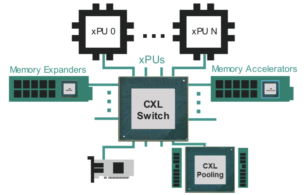
Marvell plans for CXL's introduction in the data centre

The open interconnect Compute Express Link (CXL) standard promises to change how data centre computing is architected.
CXL enables the rearrangement of processors (CPUs), accelerator chips, and memory within computer servers to boost efficiency.
“CXL is such an important technology that is in high focus today by all the major cloud hyperscalers and system OEMs,” says Thad Omura, vice president of flash marketing at Marvell.
Semiconductor firm Marvell has strengthened its CXL expertise by acquiring Tanzanite Silicon Solutions.
Tanzanite was the first company to show two CPUs sharing common memory using a CXL 2.0 controller implemented using a field-programmable gate array (FPGA).
Marvell intends to use CXL across its portfolio of products.
Terms of the deal for the 40-staff Tanzanite acquisition have not been disclosed.
Data centre challenges
Memory chips are the biggest item spend in a data centre. Each server CPU has its own DRAM, the fast volatile memory overseen by a DRAM controller. When a CPU uses only part of the memory, the rest is inactive since other server processors can’t access it.
“That’s been a big issue in the industry; memory has consistently been tied to some sort of processor,” says Omura.
Maximising processing performance is another issue. Memory input-output (I/O) performance is not increasing as fast as processing performance. Memory bandwidth available to a core has thus diminished as core count per CPU has increased. “These more powerful CPU cores are being starved of memory bandwidth,” says Omura.
CXL tackles both issues: it enables memory to be pooled improving usage overall while new memory data paths are possible to feed the cores.
CXL also enables heterogeneous compute elements to share memory. For example, accelerator ICs such as graphic processing units (GPUs) working alongside the CPU on a workload.
CXL technology
CXL is an industry-standard protocol that uses the PCI Express (PCIe) bus as the physical layer. PCI Express is used widely in the data centre; PCIe 5.0 is coming to market, and the PCIe 6.0 standard, the first to use 4-level pulse-amplitude modulation (PAM-4), was completed earlier this year.
In contrast, other industry interface protocols such as OpenCAPI (open coherent accelerator processor interface) and CCIX (cache coherent interconnect for accelerators) use custom physical layers.
“The [PCIe] interface feeds are now fast enough to handle memory bandwidth and throughput, another reason why CXL makes sense today,” says Omura.
CXL supports low-latency memory transactions in the tens of nanoseconds. In comparison, the non-volatile memory express storage (NVMe), which uses a protocol stack run on a CPU, has tens of microseconds transaction times.
“The CXL protocol stack is designed to be lightweight,” says Omura. “It doesn’t need to go through the whole operating system stack to get a transaction out.”
CXL enables cache coherency, which is crucial since it ensures that the accelerator and the CPU see the same data in a multi-processing system.
Memory expansion
The first use of CXL will be to simplify the adding of memory.
A server must be opened when adding extra DRAM using a DIMM (dual in-line memory module). And there are only so many DIMM slots in a server.
The DIMM also has no mechanism to pass telemetry data such as its service and bit-error history. Cloud data centre operators use such data to oversee their infrastructure.
Using CXL, a memory expander module can be plugged into the front of the server via PCIe, avoiding having to open the server. System cooling is also more straightforward since the memory is far from the CPU. The memory expander’s CXL controller can also send telemetry data.
CXL also boosts memory bandwidth. When adding a DIMM to a CPU, the original and added DIMM share the same channel; capacity is doubled but not the interface bandwidth. Using CXL however opens a channel as the added memory uses the PCIe bus.
“If you’re using the by-16 ports on a PCIe generation five, it [the interface] exceeds the [DRAM] controller bandwidth,” says Omura.
Pooled memory
CXL also enables memory pooling. A CPU can take memory from the pool for a task, and when completed, it releases the memory so that another CPU can use it. Future memory upgrades are then added to the pool, not an individual CPU. “That allows you to scale memory independently of the processors,” says Omura.
The likely next development is for all the CPUs to access memory via a CXL switch. Each CPU will no longer needs a local DRAM controller but rather it can access a memory expander or the memory pool using the CXL fabric (see diagram above).
Going through a CXL switch adds latency to the memory accesses. Marvell says that the round trip time for a CPU to access its local memory is about 100ns, while going through the CXL switch to pooled memory is projected to take 140-160ns.
The switch can also connect a CXL accelerator. Here, an accelerator IC is added to memory which can be shared in a cache coherent manner with the CPU through the switch fabric (see diagram above).
I/O acceleration hardware can also be added using the CXL switch. Such hardware includes Ethernet, data processing unit (DPU) smart network interface controllers (smartNICs), and solid-state drive (SSD) controllers.
“Here, you are focused on accelerating protocol-level processing between the network device or between the CPU and storage,” says Omura. These I/O devices become composable using the CXL fabric.
More CXL, less Ethernet
Server boxes in the data are stacked. Each server comprises CPUs, memory, accelerators, network devices and storage. The servers talk to each other via Ethernet and other server racks using a top-of-rack switch.
But the server architecture will change as CXL takes hold in the data centre.

“As we add CXL into the infrastructure, for the first time, you’re going to start to see disaggregate memory,” says Omura. “You will be able to dynamically assign memory resources between servers.”
For some time yet, servers will have dedicated memory. Eventually, however, the architecture will become disaggregated with separate compute, memory and I/O racks. Moreover, the interconnect between the boxes will be through CXL. “Some of the same technology that has been used to transmit high-speed Ethernet will also be used for CXL,” says Omura.
Omura says deployment of the partially-disaggregated rack will start in 2024-25, while complete disaggregation will likely appear around the decade-end.
Co-packaged optics and CXL
Marvell says co-packaging optics will fit well with CXL.

“As you disaggregate memory from the CPU, there is a need to have electro-optics drive distance and bandwidth requirements going forward,” says Nigel Alvares, vice president of solutions marketing at Marvell.
However, CXL must be justified from a cost and latency standpoint, limiting its equipment-connecting span.
“The distance in which you can transmit data over optics versus latency and cost is all being worked out right now,” says Omura. The distance is determined by the transit time of light in fibre and the forward error correction scheme used.
But CXL needs to remain very low latency because memory transactions are being done over it, says Omura: “We’re no longer fighting over just microseconds or milliseconds of networking, now we’re fighting over nanoseconds.”
Marvell can address such needs with its acquisition of Inphi and its PAM-4 and optical expertise, the adoption of PAM-4 encoding for PCIe 6.0, and now the addition of CXL technology.

Marvell's first Inphi chips following its acquisition

Marvell unveiled three new devices at the recent OFC virtual conference and show.
One chip is its latest coherent digital signal processor (DSP), dubbed Deneb. The other two chips, for use within the data centre, are a PAM-4 (4-level pulse-amplitude modulation) DSP, and a 1.6-terabit Ethernet physical layer device (PHY).
The chips are Marvell’s first announced Inphi products since it acquired the company in April. Inphi’s acquisition adds $0.7 billion to Marvell’s $3 billion annual revenues while the more than 1,000 staff brings the total number of employees to 6,000.
Marvell spends 30 per cent of its revenues on R&D.
Acquisitions
Inphi is the latest of a series of Marvell acquisitions as it focusses on data infrastructure.
Marvell acquired two custom ASIC companies in 2019: Avera Semiconductor, originally the ASIC group of IBM Microelectronics, and Aquantia that has multi-gigabit PHY expertise.
A year earlier Marvell acquired processing and security chip player, Cavium Networks. Cavium had acquired storage specialist, QLogic, in 2017.
These acquisitions have more than doubled Marvell’s staff. Inphi brings electro-optics expertise for the data centre and optical transport and helps Marvell address the cloud and on-premises data centre markets as well as the 5G carrier market.
Marvell is also targeting the enterprise/ campus market and what it highlights as a growth area, automotive. Nigel Alvares, vice president of solutions at Marvell, notes the growing importance of in-vehicle networking, what he calls a ‘data-centre-on-wheels’.
“Inphi’s technology could also help us in automotive as optical technologies are used for self-driving initiatives in future,” says Alvares.
Inphi also brings integration, co-packaging and multi-chip module expertise.

Merchant chip and custom ASIC offerings
Cloud operators and 5G equipment vendors are increasingly developing custom chip designs. Marvell says it is combining its portfolio with their intellectual property (IP) to develop and build custom ICs.
Accordingly, in addition to its merchant chips such as the three OFC-announced devices, Marvell partners with cloud players or 5G vendors, providing them with key IP blocks that are integrated with their custom IP. Marvell can also build the ASICs.
Another chip-design business model Marvell offers is the integration of different hardware in a multi-chip package. The components include a custom ASIC, merchant silicon, high-speed memory and third-party chiplets.
“We co-package and deliver it to a cloud hyperscaler or a 5G technical company,” says Alvares.
Marvell says this chip strategy serves two market sectors: the cloud hyperscalers and the telcos.
Cloud players are developing custom solutions as they become more vertically integrated. They also have deep pockets. But they can’t do everything because they are not chip experts so they partner with companies like Marvell.
“The five to 10 hyperscalers in the world, they are doing so much creative stuff to optimise applications that they need custom silicon,” says Alvares.
The telcos, in contrast, are struggling to grow their revenues and favour merchant ICs, given they no longer have the R&D budgets of the past. It is this split in the marketplace which Marvell is targeting its various chip services.
OFC announcements
At OFC, Marvell announced the Deneb coherent DSP, used for optical transport including the linking of equipment between data centres.
The Deneb DSP is designed with open standards in mind and complements the 400-gigabit CMOS Canopus DSP announced by Inphi in 2019.
Deneb adds the oFEC forward error correction scheme to support open standards such as OpenZR+, 100-gigabit ZR, the 400-gigabit OpenROADM MSA and CableLabs’ 100-gigabit standard.
The 100-gigabit ZR is targeted at the 5G access market and mobile backhaul. Like the OIF 400G ZR, it supports reaches of 80-120km but uses quadrature phase-shift keying (QPSK) modulation.
“Not only do we support 100 gigabit [coherent] but we also have added the full industrial temperature range, from -40oC to 85oC,” says Michael Furlong, associated vice president, product marketing at Marvell.
The Deneb DSP is sampling now. Both the Deneb and Canopus DSPs will have a role in the marketplace, says Furlong.

Atlas PAM-4 DSP and the 1.6-terabit PHY
Marvell also announced at OFC the Atlas PAM-4 DSP and a dual 800-gigabit PHY devices used within the data centre.
Atlas advances Marvell’s existing family of Polaris PAM-4 DSPs in that it integrates physical media devices. “We are integrating [in CMOS] the trans-impedance amplifier (TIA) and laser drivers,” says Alvares.
Using the 200-gigabit Atlas reduces an optical module design from three chips to two; the Atlas comprises a transmit chip and a receiver chip (see diagram below). Using the Atlas chips reduces the module’s bill of materials, while power consumption is reduced by a quarter.

The Atlas chips, now sampling, are not packaged but offered as bare die and will be used for 200-gigabit SR4 and FR4 modules. Meanwhile, Marvell’s 1.6-terabit PHY – the 88X93160, – is a dual 800-gigabit copper DSP that performs retimer and gearbox functions.
“We view this as the key data centre building block for the next decade,” says Alvares. “The world is just starting to design 100-gigabit serial for their infrastructure.”
The device, supporting 16, 100-gigabit lanes, is the industry’s first 100-gigabit serial retimer, says Marvell. The device drives copper cable and backplanes and is being adopted for links between the server and the top-of-tack switch or to connect switches in the data centre.
The device is suitable for next-generation 400-gigabit and 800-gigabit Ethernet links that use 100-gigabit electrical serialisers-deserialisers (serdes).
The 5nm CMOS device supports over a 38dB (decibel) link budget and reduces I/O power by 40 per cent compared to a 50-gigabit Nigel PAM4-based PHY.
The 100-gigabit serdes design will also be used with Marvell’s Prestera switch portfolio.

Telecoms embraces 400ZR optics for IP-over-DWDM

Verizon Media has trialled 400-gigabit coherent pluggable optics to improve the delivery of video content to subscribers.
Verizon Media added a 400ZR QSFP-DD module from Inphi to a switch already using 100-gigabit optics.
Adding dense wavelength-division multiplexing (DWDM) optics to a switch enables it to send IP traffic (IP-over-DWDM) directly without needing a separate DWDM data centre interconnect box and additional client-side optics to link the two platforms (see diagram).
“Verizon Media, showing leadership outside the hyperscalers, is moving to IP-over-DWDM,” says Tomas Maj, senior director, marketing, optical interconnect at Inphi. “It shows the maturity of the ecosystem and the confidence of more and more operators in IP-over-DWDM and 400ZR.”
Content distribution network
Inphi cites three applications driving traffic growth between data centres: cloud network virtualisation, content distribution and edge analytics, and data mirroring and backup.
The primary users of these applications are the hyperscalers – it is the hyperscalers that spurred the creation of the OIF’s 120km 400ZR standard – but these applications increasingly apply to the telcos.
Verizon Media uses its content delivery network to share and back-up video between its data centres dubbed super PoPs (points-of-presence). Video is also sent to smaller outlying sites, closer to subscribers, where the most popular content is hosted.
ColorZ II
Verizon Media’s network uses Inphi’s existing 100-gigabit ColorZ QSFP28 pluggable optics.
The ColorZ is a direct-detect module that uses 4-level pulse amplitude modulation (PAM-4) to convert 4×25-gigabit electrical signals to two 50-gigabit PAM-4 optical wavelengths that fit within a 100GHz channel.
The ColorZ module, of which Inphi has now shipped over 100,000 units, has an 80km reach.
Inphi’s second-generation ColorZ II uses the OIF’s 400ZR coherent standard. Both generations employ an silicon photonics chip to implement the optics.
“As you go up in PAM-4 speed, you are taking hits in optical signal-to-noise ratio and receiver sensitivity and the design becomes costly,” says Maj. “At some point, you look at coherent and you have better yield and optical performance.”
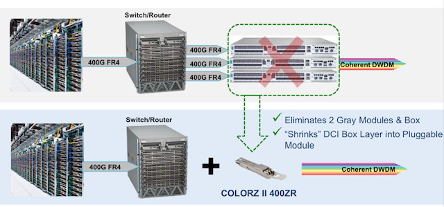
For Verizon Media’s trial, the ColorZ II 400ZR QSFP-DD was added to switches from Arista Networks. Using ColorZ II optics in the same 100GHz channels quadruples fibre capacity from 4 to 16 terabits while halving the transmission cost-per-bit.
Nitin Batta, principal infrastructure architect at Verizon Media, said in a press release that the ColorZ II was chosen to enable it to “rapidly, easily and cost-effectively add terabits of capacity in response to customer demand.”
The 400ZR standard ensures interoperability and gives customers confidence by having several module companies to choose from, says Maj. Adopting the module also provides important diagnostic information regarding a link’s performance.
All the elements for a 400-gigabit ecosystem are coming together, says Inphi.
Four-hundred-gigabit client-side optical modules are leading the way and now 400-gigabit coherent pluggables are at the testing and validation stage before volume deployment.
The ColorZ II will be generally available at the year’s end.
Inphi unveils first 800-gigabit PAM-4 signal processing chip
Inphi has detailed what it claims is the industry’s first digital signal processor (DSP) chip family for 800-gigabit client-side pluggable modules.
Dubbed Spica, the 4-level pulse-amplitude modulation (PAM-4) DSP family is sampling and is in the hands of customers.
The physical-layer company has also announced its third-generation Porrima family of PAM-4 DSPs for 400-gigabit pluggables.
The Porrima DSP with integrated laser driver has being made using a 7nm CMOS process; until now a 16nm CMOS has been used. Fabricating the chip using the more advanced process will reduce the power consumption of 400-gigabit module designs.
Applications
Eight-hundred-gigabit multi-source agreements (MSAs) will enable a new generation of high-speed optical transceivers to come to market.
The 800G Pluggable MSA developing optical specifications for 800-gigabit pluggable modules, is one that Inphi is promoting, while the QSFP-DD800 MSA is extending the double density form factor for 800 gigabits.

The main two markets driving a need for 800-gigabit modules are artificial intelligence (AI) and data centre switching, says Eric Hayes, senior vice president, networking interconnect at Inphi.
“AI, while still in its infancy, has all these applications and workloads that it can drive,” he says. “But one thing they have in common when we look at the data centres building large AI clusters is that they have very large data sets and lots of data flow.”
The speed of the input-output (I/O) of the AI processors used in the clusters is rising to cope with the data flows.
The second application that requires 800-gigabit modules is the advent of 25.6-terabit Ethernet switches used to network equipment within the data centre.
Inphi says there are two types of 25.6-terabit switch chips emerging: one uses 50-gigabit PAM-4 while the second uses 100-gigabit PAM-4 electrical interfaces.
“The 25.6-terabyte switch with 100-gigabit I/O is wanted for one-rack-unit (1RU) platforms,” says Hayes. “To do that, you need an 800-gigabit module.” Such switches have yet to reach the marketplace.
The first-generation AI processors used 25-gigabit non-return-to-zero (NRZ) signalling for the I/O while many of the devices shipping today use 50-gigabit PAM-4. “The latest designs that are coming to market have 100-gigabit I/O and we have the first DSP offering 100-gigabit on the host side,” says Hayes.
Spica and Porrima ICs
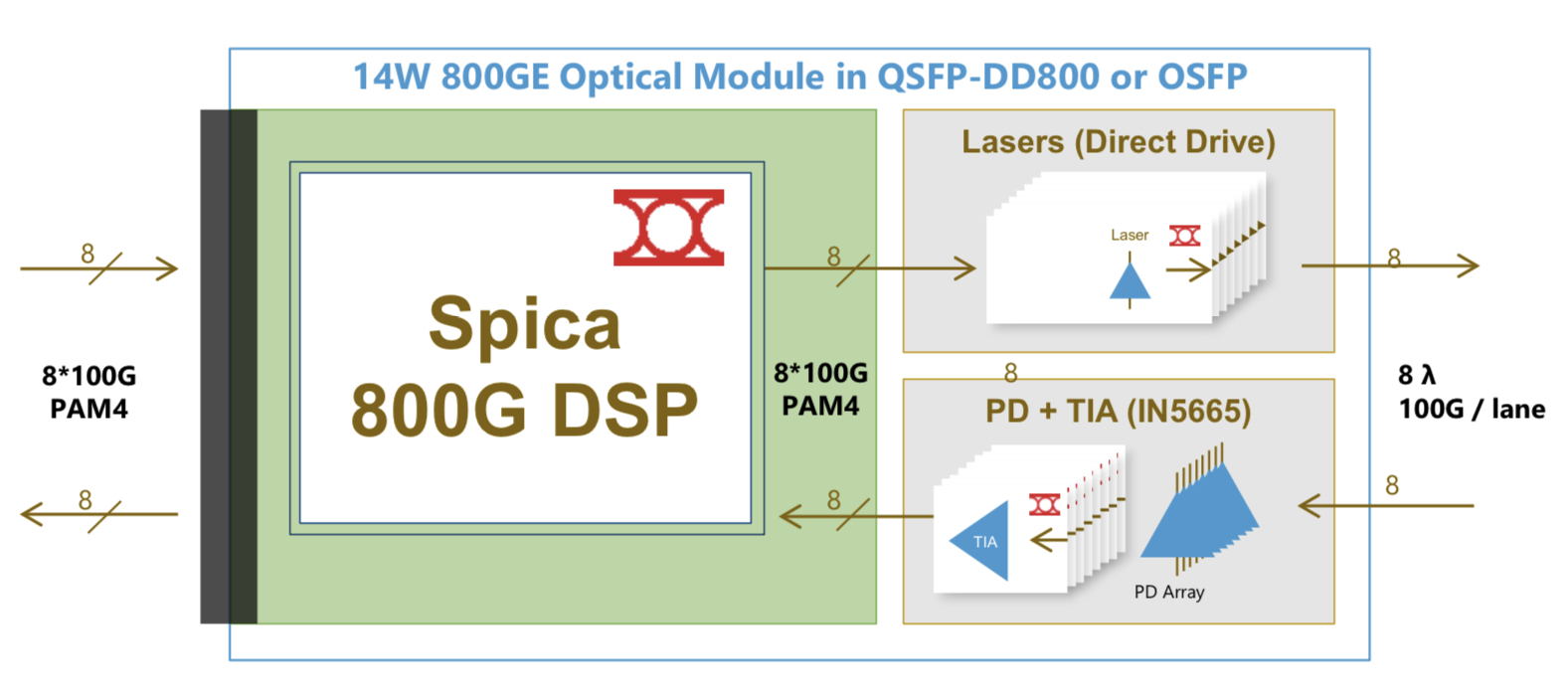
The Spica DSP takes 100-gigabits PAM-4 electrical signals from the host and performs retiming and pre-emphasis to generate the 100-gigabit PAM-4 signals used for modulation the optics before transmission. The laser driver is integrated on-chip.
The transmit path is a simpler design than the Porrima in that the signalling rate is the same at the input and the output. Accordingly, no gearbox circuitry is needed.
The main signal processing is performed at the receiver to recover the sent PAM-4 signals. A hybrid design is used combining analogue and digital signal processing, similar to the design used for the Porrima.
The Spica device supports 2×400-gigabit or 8×100-gigabit module designs and enables 800-gigabit or 8×100-gigabit optical interconnects. The 800-gigabit form factors used are the QSFP-DD800 and the OSFP. Inphi says both designs consume under 14W.
“The first module being built [using the Spica] is the OSFP because the end-user is demanding that, but we also have customers building QSFP-DDs,” says Hayes.
Meanwhile, Inphi’s Porrima family of devices is targeted at the 400G DR4 and 400G FR4 specifications as well as 100-gigabit module designs that use 100-gigabit PAM-4.
The two module types can even be combined when a 400-gigabit pluggable such as a QSFP-DD or an OSFP is used in breakout mode to feed four 100-gigabit modules implement using such form factors as the QSFP, uQSFP or SFP-DD.
Transitioning the Porrima to a 7nm process saves 1.5W of power, says Hayes, resulting in an 8W 400-gigabit module. The latest Porrima is sampling and is with customers.
Roadmap
Inphi says optical modules using the Spica DSP will be deployed in volume from the second half of 2021.
Before then, the DSP will be tested as part of customers’ module designs, then be integrated with the software before the complete 800-gigabit module is tested.
“There will then be interoperability testing between the modules once they become available and then small pilot networks using 800-gigabit modules will be built and tested before the go-ahead to mass deployment,” says Hayes.
All these stages will require at least a year’s work.

The era of 400G coherent pluggables finally emerges

Part 1: 7nm coherent DSPs, ZR and ZR+
The era of 400-gigabit coherent pluggable modules has moved a step closer with Inphi’s announcement of its Canopus coherent digital signal processor (DSP) and its QSFP-DD ColorZ II optical module.
NeoPhotonics has also entered the fray, delivering first samples of its 400-gigabit ClearLight CFP2-DCO module that uses the Canopus DSP.
The ColorZ II and ClearLight modules support the 400ZR OIF standard used to link data centres up to 120km apart. They also support extended modes, known as ZR+, that is not standardised.
ZR+’s modes include 400 Gigabit-per-second (Gbps) over distances greater than 400ZR’s 120km and lower data rates over metro-regional and long-haul distances.
The announcements of the Canopus DSP and 400-gigabit pluggable coherent modules highlight the approaches being taken for ZR+. Optical module vendors are aligning around particular merchant DSPs such that interoperability exists but only within each camp.
The first camp involves Inphi and three other module vendors, one being NeoPhotonics. The second camp is based on the OpenZR+ specification that offers interoperability between the DSPs of the merchant players, Acacia Communications and NTT Electronics (NEL). Cisco is in the process of acquiring Acacia.
Market analysts, however, warn that such partial interoperability for ZR+ harms the overall market opportunity for coherent pluggables.
“ZR+ should be interoperable like ZR, and come along with the hard decisions the ZR standard required,” says Andrew Schmitt, founder and directing analyst at research form, Cignal AI.

The optical module vendors counter that only with specialist designs – designs that are multi-sourced – can the potential of a coherent DSP be exploited.
Applications
The advent of 400-gigabit coherent optics within compact client-side form factors is a notable development, says Inphi. “The industry has been waiting for this inflextion point of having, for the first time, 400-gigabit coherent pluggables that go on router and switch interfaces,” says Pranay Aiya, vice president of product marketing and applications engineering at Inphi.
“IP over DWDM has never happened; we have all heard about it till the cows come home,” says Aiya.
IP-over-DWDM failed to take off because of the power and space demands of coherent optics, especially when router and switch card slots come at a premium. Using coherent optics on such platforms meant trading off client-side faceplate capacity to fit bulkier coherent optics. This is no longer the case with the advent of QSFP-DD and OSFP coherent modules.
“If you look at the reasons why IP-over-DWDM – coloured optics directly on routers – failed, all of those reasons have changed,” says Schmitt. The industry is moving to open line systems, open network management, and more modular network design.
“All of the traffic is IP and layer-1 switching and grooming isn’t just unnecessary, it is more expensive than low-feature layer-2 switching,” says Schmitt, adding that operators will use pluggables wherever the lower performance is acceptable. Moreover, this performance gap will narrow with time.
The Canopus DSP also supports ZR+ optical performance and, when used within a CFP2-DCO module with its greater power enveloped than OSFP and QSFP-DD, enables metro and long-haul distances, as required by the telecom operators. This is what Neophotonics has announced with its ClearLight CFP2-DCO module.

Canopus
Inphi announced the Canopus DSP last November and revealed a month later that it was sampling its first optical module, the ColorZ II, that uses the Canopus DSP. The ColorZ II is a QSFP-DD pluggable module that supports 400ZR as well as the ZR+ extended modes.
Inphi says that, given the investment required to develop the 7nm CMOS Canopus, it had to address the bulk of the coherent market.
“We were not going after the ultra-long-haul and submarine markets but we wanted pluggables to address 80-90 per cent of the market,” says Aiya.
This meant developing a chip that would support the OIF’s 400ZR, 200-gigabit using quadrature phased-shift keying (QPSK) modulation for long haul, and deliver 400-gigabit over 500-600km.
The Canopus DSP also supports probabilistic constellation shaping (PCS), a technology that until now has been confined to the high-end coherent DSPs developed by the leading optical systems vendors.
With probabilistic shaping, not all the constellation points are used. Instead, those with lower energy are favoured; points closer to the origin on a constellation graph. The only time all the constellation points are used is when sending the maximum data rate for a given modulation scheme.
Choosing the inner, lower-energy constellation points more frequently than the outer points to send data reduces the average energy and improves the signal-to-noise ratio. To understand why, the symbol error rate at the receiver is dominated by the distance between neighbouring points on the constellation. Reducing the average energy keeps the distance between the points the same, but since a constant signal power level is used for DWDM transmission, applying gain increases the distance between the constellation points. The result is improved optical performance.
Probabilistic shaping also allows an exact number of bits-per-symbol to be sent, even non-integer values.

For example, using standard modulation schemes such as 64-QAM with no constellation shaping, 6 bits-per-symbol are sent. Using shaping and being selective as to which constellation points are used, 5.7 bits-per-symbol could be sent, for example. This enables finer control of the sent data, enabling operators to squeeze the maximum data rate to suit the margins on a given fibre link.
“This is the first time a DSP with probabilistic shaping has been available in a size and power that enables pluggables,” says Aiya.
The resulting optical performance using the Canopus is up to 1,500km at 300Gbps signals and up to 2,000km for 200Gbps transmissions (see Table above). As for baud rates, the DSP ranges from 30+ to the mid-60s Gigabaud.
Inphi also claims a 75 per cent reduction in power consumption of the Canopus compared to 16nm CMOS DSPs found in larger, 4×5-inch modules.
Several factors account for the sharp power reduction: the design of the chip’s architecture and physical layout, and the use of 7nm CMOS. The Canopus uses functional blocks that extend the reach, and these can be turned off to reduce the power consumption when lower optical performance is acceptable.
The architectural improvements and the physical layout account for half of the overall power savings, says Aiya, with the rest coming from using a 7nm CMOS.
The result is a DSP a third the size of 16nm DSPs. “It [pluggables] requires the DSP to be very small; it’s not a paperweight anymore,” says Aiya.
400ZR and ZR+
The main challenge for the merchant coherent DSP camps is the several, much larger 400ZR eco-systems from Ciena, Cisco and Huawei.
“Each one of these eco-systems will be larger than the total merchant market of 400ZR,” says Vladimir Kozlov, CEO and founder of LightCounting. The system vendors will make sure that their products offer something extra if plugged into their equipment while maintaining interoperability. “This could be some simple AI-like features monitoring the link performance and warning customers of poor operation of devices on the other side of the link if these are made by another supplier,” says Kozlov.
LightCounting says that ZR+ units will be half to a third of the the number of 400ZR units shipped. However, each ZR+ module will command a higher selling price.
Regarding the ZR+ camps, one standardisation effort is OpenZR+ that adopts the forward-error correction (oFEC) scheme of the OpenROADM MSA, supports multiplexing of 100 Gigabit Ethernet (GbE) and 200GbE client signals, and different line rates – 100-400Gbps – to achieve greater reaches.
The backers of OpenZR+ include the two merchant DSP vendors, Acacia and NEL, as well as Fujitsu Optical Components, Lumentum, and Juniper Networks.
The second ZR+ camp includes four module-makers that are adopting the Canopus: Inphi, Molex Optoelectronics, NeoPhotonics and an unnamed fourth company. According to Schmitt, the unnamed module maker is II-VI. II-VI declined to comment when asked to confirm.
Schmitt argues that ZR+ should be interoperable, just like 400ZR. “I think NEL, Acacia, and Inphi should have an offsite and figure this out,” he says. “These three companies are in a position to nail down the specs and create a large, disruptive coherent pluggable market.”

Simon Stanley, founder and principal consultant at Earlswood Marketing Limited, expects several ZR+ solutions to emerge but that the industry will settle on a common approach. “You will initially see both ZR+ and OpenZR+,” says Stanley. “ZR+ will be specific to each operator but over time I expect OpenZR+ or something similar to become the standard solution.”
But the optical vendors stress the importance of offering differentiated designs to exploit the coherent DSP’s full potential. And maximising a module’s optical performance is something operators want.
“We are all for standards where it makes sense and where customers want it,” says Inphi’s Aiya. “But for customers that require the best performance, we are going to offer them an ecosystem around this DSP.”
“It is always a trade-off,” adds Ferris Lipscomb, vice president of marketing at NeoPhotonics. “More specialised designs that aren’t interoperable can squeeze more performance out; interoperable has to be the lowest common denominator.”
Next-generation merchant DSPs
The next stage in coherent merchant DSP development is to use a 5nm CMOS process, says Inphi. Such a state-of-the-art [CMOS] process will be needed to double capacity again while keeping the power consumption constant.
The optical performance of a 5nm coherent DSP in a pluggable will approach the high-end coherent designs. “It [the optical performance of the two categories] is converging,” says Aiya.
However, demand for such a device supporting 800 gigabits will take time to develop. Several years have passed for demand for 400-gigabit client-side optics to ramp and there will be a delay before telecom operators need 400-gigabit wavelengths in volume, says Inphi.
LightCounting points out that it will take Inphi and its ecosystem of suppliers at least a year to debug their products and demonstrate interoperability.
“And keep in mind that we are talking about the industry that is changing very slowly,” concludes Kozlov.


Data centre interconnect drives coherent
-
NeoPhotonics announced at OFC a high-speed modulator and intradyne coherent receiver (ICR) that support an 800-gigabit wavelength
-
It also announced limited availability of its nano integrable tunable laser assembly (nano-ITLA) and demonstrated its pico-ITLA, an even more compact silicon photonics-based laser assembly
-
The company also showcased a CFP2-DCO pluggable
NeoPhotonics unveiled several coherent optical transmission technologies at the OFC conference and exhibition held in San Diego last month.
“There are two [industry] thrusts going on right now: 400ZR and data centre interconnect pizza boxes going to even higher gigabits per wavelength,” says Ferris Lipscomb, vice president of marketing at NeoPhotonics.

Ferris Lipscomb
The 400ZR is an interoperable 400-gigabit coherent interface developed by the Optical Internetworking Forum (OIF).
Optical module makers are developing 400ZR solutions that fit within the client-side QSFP-DD and OSFP pluggable form factors, first samples of which are expected by year-end.
800-gigabit lambdas
Ciena and Infinera announced in the run-up to OFC their latest coherent systems - the WaveLogic 5 and ICE6, respectively - that will support 800-gigabit wavelengths. NeoPhotonics announced a micro intradyne coherent receiver (micro-ICR) and modulator components that are capable of supporting such 800-gigabit line-rate transmissions.
NeoPhotonics says its micro-ICR and coherent driver modulator are class 50 devices that support symbol rates of 85 to 90 gigabaud required for such a state-of-the-art line rate.
The OIF classification defines categories for devices based on their analogue bandwidth performance. “With class 20, the 3dB bandwidth of the receiver and the modulator is 20GHz,” says Lipscomb. “With tricks of the trade, you can make the symbol rate much higher than the 3dB bandwidth such that class 20 supports 32 gigabaud.” Thirty-two gigabaud is used for 100-gigabit and 200-gigabit coherent transmissions.
Class 50 refers to the highest component performance category where devices have an analogue bandwidth of 50GHz. This equates to a baud rate close to 100 gigabaud, fast enough to achieve data transmission rates exceeding a terabit. “But you have to allow for the overhead the forward-error correction takes, such that the usable data rate is less than the total,” says Lipscomb (see table).

Source: Gazettabyte, NeoPhotonics
Silicon photonics-based COSA
NeoPhotonics also announced a 64-gigabaud silicon photonics-based coherent optical subassembly (COSA). The COSA combines the receiver and modulator in a single package that is small enough to fit within a QSFP-DD or OSFP pluggable for applications such as 400ZR.
Last year, the company announced a similar COSA implemented in indium phosphide. In general, it is easier to do higher speed devices in indium phosphide, says Lipscomb, but while the performance in silicon photonics is not quite as good, it can be made good enough.
“It [silicon photonics] is now stretching certainly into the Class 40 [that supports 600-gigabit wavelengths] and there are indications, in certain circumstances, that you might be able to do it in the Class 50.”
Lipscomb says NeoPhotonics views silicon photonics as one more material that complements its indium phosphide, planar lightwave circuit and gallium arsenide technologies. “Our whole approach is that we use the material platform that is best for a certain application,” says Lipscomb.
In general, coherent products for telecom applications take time to ramp in volumes. “With the advent of data centre interconnect, the volume growth is much greater than it ever has been in the past,” says Lipscomb.
NeoPhotonics’ interested in silicon photonics is due to the manufacturing benefits it brings that help to scale volumes to meet the hyperscalers’ requirements. “Whereas indium phosphide has very good performance, the infrastructure is still limited and you can’t duplicate it overnight,” says Lipscomb. “That is what silicon photonics does, it gives you scale.”
NeoPhotonics also announced the limited availability of its nano integrable tunable laser assembly (nano-ITLA). “This is a version of our external cavity ITLA that has the narrowest line width in the industry,” says Lipscomb.
The nano-ITLA can be used as the source for Class 50, 800-gigabit systems and current Class 40 600 gigabit-per-wavelength systems. It is also small enough to fit within the QDFP-DD and OSFP client-side modules for 400ZR designs. “It is a new compact laser that can be used with all those speeds,” says Lipscomb.
NeoPhotonics also showed a silicon-photonics based pico-ITLA that is even smaller than the nano-ITLA.“The [nano-ITLA’s] optical cavity is now made using silicon photonics so that makes it a silicon photonics laser,” says Lipscomb.
Instead of having to assemble piece parts using silicon photonics, it can be made as one piece. “It means you can integrate that into the same chip you put your modulator and receiver on,” says Lipscomb. “So you can now put all three in a single COSA, what is called the IC-TROSA.” The IC-TROSA refers to an integrated coherent transmit-receive optical subassembly, defined by the OIF, that fits within the QSFP-DD and OSFP.
Despite the data centre interconnect market with its larger volumes and much faster product uptakes, indium phosphide will still be used in many places that require higher optical performance. “But for bulk high-volume applications, there are lots of advantages to silicon photonics,” says Lipscomb.
400ZR and 400ZR+
A key theme at this year’s OFC was the 80km 400ZR. Also of industry interest is the 400ZR+, not an OIF specification but an interface that extends the coherent range to metro distances.
Lipscomb says that the initial market for the 400ZR+ will be smaller than the 400ZR, while the ZR+’s optical performance will depend on how much power is left after the optics is squeezed into a QSFP-DD or OSFP module.
“The next generation of DSP will be required to have a power consumption low enough to do more than ZR distances,” he says. “The further you go, the more work the DSP has to do to eliminate the fibre impairments and therefore the more power it will consume.”
Will not the ZR+ curtail the market opportunity for the 400-gigabit CFP2-DCO that is also aimed at the metro?
“It’s a matter of timing,” says Lipscomb. “The advantage of the 400-gigabit CFP2-DCO is that you can almost do it now, whereas the ZR+ won’t be in volume till the end of 2020 or early 2021.”
Meanwhile, NeoPhotonics demonstrated at the show a CFP2-DCO capable of 100-gigabit and 200-gigabit transmissions.
NeoPhotonics has not detailed the merchant DSP it is using for its CFP2-DCO except to say that it working with ‘multiple ones’. This suggests it is using the merchant coherent DSPs from NEL and Inphi.

Inphi adds a laser driver to its 100-gigabit PAM-4 DSP
Inphi has detailed its second-generation Porrima chip family for 100-gigabit single-wavelength optical module designs.

Source: Inphi
The Porrima family of devices is targeted at the 400G DR4 and 400G FR4 specifications as well as 100-gigabit module designs that use 100-gigabit 4-level pulse-amplitude modulation (PAM-4). Indeed, the two module types can be combined when a 400-gigabit pluggable such as a QSFP-DD or an OSFP is used in breakout mode to feed four 100-gigabit modules using such form factors as the QSFP, uQSFP or SFP-DD.
The Gen2 family has been launched a year after the company first announced the Porrima. The original 400-gigabit and 100-gigabit Porrima designs each have three ICs: a PAM-4 digital signal processor (DSP), a trans-impedance amplifier (TIA) and a laser-driver.
“With Gen2, the DSP and laser driver are integrated into a single monolithic CMOS chip, and there is a separate amplifier chip,” says Siddharth Sheth, senior vice president, networking interconnect at Inphi. The benefit of integrating the laser driver with the DSP is lower cost, says Sheth, as well as a power consumption saving.
The second-generation Porrima family is now sampling with general availability expected in mid-2019.
PAM-4 families
Inphi has three families of PAM-4 ICs targeting 400-gigabit interfaces: the Polaris, Vega and Porrima.
The Polaris, Inphi’s first product family, uses a 200-gigabit die and two are used within the same package for 400-gigabit module designs. As well as the PAM-4 DSP, the Polaris family also comprises two companion chips: a laser driver and an amplifier.
Inphi’s second family is the Vega, a 8x50-gigabit PAM-4 400-gigabit DSP chip that sits on a platform’s line card.
“The chip is used to drive backplanes and copper cables and can be used as a retimer chip,” says Sheth.
Siddharth Sheth
“For the Porrima family, you have a variant that does 4x100-gigabit and a variant that does 1x100-gigabit,” says Sheth. The Porrima can interface to a switch chip that uses either 4x25-gigabit non-return-to-zero (NRZ) or 2x50-gigabit PAM-4 electrical signals.
Why come out with a Gen2 design only a year after the first Porrima? Sheth says there was already demand for 400-gigabit PAM-4 chips when the Porrima first became available in March 2018. Optical module makers needed such chips to come to market with 400-gigabit modules to meet the demand of an early hyperscale data centre operator.
“Now, the Gen2 solution is for the second wave of customers,” says Sheth. “There are going to be two or three hyperscalers coming online in 2020 but maybe not as aggressively as the first hyperscaler.” These hyperscalers will be assessing the next generation of 400-gigabit PAM-4 silicon available, he says.
The latest design, like the first generation Porrima, is implemented using 16nm CMOS. The DSP itself has not been modified; what has been added is the laser-driver circuitry. Accordingly, it is the transmitter side that has been changed, not the receiver path where Inphi does the bulk of the signal processing. “We did not want to change a whole lot because that would require a change to the software,” he says.
A 400-gigabit optical module design using the first generation Porrima consumes under 10W but only 9W using the Gen2. The power saving is due to the CMOS-based laser driver consuming 400mW only compared to a gallium arsenide or silicon germanium-based driver IC that consumes between 1.6W to 2W, says Inphi.
The internal driver can achieve transmission distances of 500m while a standalone driver will still be needed for longer 2km spans.
Sheth says that the advent of mature low-swing-voltage lasers will mean that the DSP’s internal driver will also support 2km links.
PAM-4 DSP
The aim of the DSP chip is to recover the transmitted PAM-4 signal. Sheth says PAM-4 chip companies differ in how much signal processing they undertake at the transmitter and how much is performed at the receiver.
“It comes down to a tradeoff, we believe that we are better off putting the heavier signal processing on the receive side,” says Sheth.
Inphi performs some signal processing on the transit side where transmit equalisation circuits are used in the digital domain, prior to the digital-to-analogue converter.
The goal of the transmitter is to emit a signal with the right amplitude, pre-emphasis, and having a symmetrical rise and fall. But even generating such a signal, the PAM-4 signal recovered at the receiver may look nothing like the signal sent due to degradations introduced by the channel. “So we have to do all kind of tricks,” he says.
Inphi uses a hybrid approach at the receiver where some of the signal processing is performed in the analogue domain and the rest digitally. A variable-gain amplifier is used up front to make sure the received signal is at the right amplitude and then feed-forward equalisation is performed. After the analogue-to-digital stage, post equalisation is performed digitally.
Sheth says that depending on the state of the received signal - the distortion, jitter and loss characteristics it has - different functions of the DSP may be employed.
One such DSP function is a reflection canceller that is turned on, depending on how much signal reflection and crosstalk occur. Another functional block that can be employed is a maximum likelihood sequence estimator (MLSE) used to recover a signal sent over longer distances. In addition, forward-error correction blocks can also be used to achieve longer spans.
“We have all sorts of knobs built into the chip to get an error-free link with really good performance,” says Sheth. “At the end of the day, it is about closing the optical link with plenty of margin.”
What next?
Sheth says the next-generation PAM-4 design will likely use an improved DSP implemented using a more advanced CMOS process.
“We will take the learning from Gen1 and Gen2 and roll it into a ‘Gen3’,” says Sheth.
Such a design will also be implemented using a 7nm CMOS process. “We are now done with 16nm CMOS,” concludes Sheth.

Inphi unveils a second 400G PAM-4 IC family
Inphi has announced the Vega family of 4-level, pulse-amplitude modulation (PAM-4) chips for 400-gigabit interfaces.
 The 16nm CMOS Vega IC family is designed for enterprise line cards and is Inphi’s second family of 400-gigabit chips that support eight lanes of 50-gigabit PAM-4.
Its first 8x50-gigabit family, dubbed Polaris, is used within 400-gigabit optical modules and was announced at the OFC show held in Los Angeles in March.
“Polaris is a stripped-down low-power DSP targeted at optical module applications,” says Siddharth Sheth, senior vice president, networking interconnect at Inphi (pictured). “Vega, also eight by 50-gigabits, is aimed at enterprise OEMs for their line-card retimer and gearbox applications.”
A third Inphi 400-gigabit chip family, supporting four channels of 100-gigabit PAM-4 within optical modules, will be announced later this year or early next year.
400G PAM-4 drivers
Inphi’s PAM-4 chips have been developed in anticipation of the emergence of next-generation 6.4-terabit and 12.8-terabit switch silicon and accompanying 400-gigabit optical modules such as the OSFP and QSFP-DD form factors.
Sheth highlights Broadcom’s Tomahawk-III, start-up Innovium’s Teralynx and Mellanox’s Spectrum-2 switch silicon. All have 50-gigabit PAM-4 interfaces implemented using 25-gigabaud signalling and PAM-4 modulation.
“What is required is that such switch silicon is available and mature in order for us to deploy our PAM-4 products,” says Sheth. “Everything we are seeing suggests that the switch silicon will be available by the end of this year and will probably go into production by the end of next year,” says Sheth.
Several optical module makers are starting to build 8x50-gigabit OSFP and QSFP-DD products
The other key product that needs to be available is the 400-gigabit optical modules. The industry is pursuing two main form factors: the OSFP and the QSFP-DD. Google and switch maker Arista Networks are proponents of the OSFP form factor while the likes of Amazon, Facebook and Cisco back the QSFP-DD. Google has said that it will initially use an 8x50-gigabit module implementation for 400 gigabit. Such a solution uses existing, mature 25-gigabit optics and will be available sooner than the more demanding 4x100-gigabit design that Amazon, Facebook and Cisco are waiting for. The 4x100 gigabit design requires 50Gbaud optics and a 50Gbaud PAM-4 chip.
Inphi says several optical module makers are starting to build 8x50-gigabit OSFP and QSFP-DD products and that its Polaris and Vega family of chips anticipate such deployments.
“We expect 100-gigabit optics to be available sometime around mid-2018 and our next-generation 100-gigabit PAM-4 will be available in the early part of next year,” says Sheth.
Accordingly, the combination of the switch silicon and optics means that the complete ecosystem will already exist next year, he says
Vega
The Polaris chip, used within an optical module, equalises the optical non-linearities of the incoming 50-gigabit PAM-4 signals. The optical signal is created using 25-gigabit lasers that are modulated using a PAM-4 signal that encodes two bits per signal. “When you run PAM-4 over fibre - whether multi-mode or single mode - the signal undergoes a lot of distortion,” says Sheth. “You need the DSP to clean up that distortion.”
The Vega chip, in contrast, sits on enterprise line cards and adds digital functionality that is not supported by the switch silicon. Most enterprise boxes support legacy data rates such as 10 gigabit and 1 gigabit. The Vega chip supports such legacy rates as well as 25, 50, 100, 200 and 400 gigabit, says Sheth.
The Vega chip can add forward-error correction to a data stream and decode it. As well as FEC, the chip also has physical coding sublayer (PCS) functionality. “Every time you need to encode a signal with FEC or decode it, you need to unravel the Ethernet data stream and then reassemble it,” says Sheth.
Also on-chip is a crossbar that can switch any lane to any other lane before feeding the data to the switch silicon.
Sheth stresses that not all switch chip applications need the Vega. For large-scale data centre applications that use stripped-down systems, the optical module would feed the PAM-4 signal directly into the switch silicon, requiring the use of the Polaris chip only.
A second role for Vega is driving PAM-4 signals across a system. “If you want to drive 50-gigabit PAM-4 signals electrically across a system line card and noisy backplane then you need a chip like Vega,” says Sheth.
A further application for the Vega chip is as a ‘gearbox’, converting between 50-gigabit and 25-gigabit line rates. Once high-capacity switch silicon with 50G PAM-4 signals are deployed, the Vega chip will enable the conversion between 50-gigabit PAM-4 and 25-gigabit non-return-to-zero (NRZ) signals.System vendors will then be able to interface 100-gigabit (4x25-gigabit) QSFP28 modules with these new switch chips.
One hundred gigabit modules will be deployed for at least another three to four years while the price of such modules has come down significantly. “For a lot of the cloud players it comes down to cost: are 128-ports at 100-gigabit cheaper that 32, 400-gigabit modules?” says Sheth. The company says it is seeing a lot of interest in this application.
We expect 100-gigabit optics to be available sometime around mid-2018 and our next-generation 100-gigabit PAM-4 will be available in the early part of next year
Availability
Inphi has announced two Vega chips: a 400-gigabit gearbox and a 400-gigabit retimer and gearbox IC. “We are sampling,” says Sheth. “We have got customers running traffic on their line cards.” General availability is expected in the first quarter of 2018.
As for the 4x100-gigabit PAM-4 chips, Sheth expects solutions to appear in the first half of next year: “We have to see how mature the optics are at that point and whether something can go into production in 2018.”
Inphi maintains that the 8x50-gigabit optical module solutions will go to market first and that the 4x100-gigabit variants will appear a year later. “If you look at our schedules, Polaris and the 4x100-gigabit PAM-4 chip are one year apart,” he says.
Coherent optics players target the network edge for growth
Part 1: Coherent developments
The market for optical links for reaches between 10km and 120km is emerging as a fierce battleground between proponents of coherent and direct-detection technologies.
Interest in higher data rates such as 400 gigabits is pushing coherent-based optical transmission from its traditional long-distance berth to shorter-reach applications. “That tends to be where the growth for coherent has come from as it has migrated from long-haul to metro,” says Tom Williams, senior director of marketing at Acacia Communications, a coherent technology supplier.
 Source: Acacia Communications, Gazettabyte
Williams points to the Optical Internetworking Forum’s (OIF) ongoing work to develop a 400-gigabit link for data centre interconnect. Dubbed 400ZR, the project is specifying an interoperable coherent interface that will support dense wavelength-division multiplexing (DWDM) links for distances of at least 80km.
Meanwhile, the IEEE standards group defining 400 Gigabit Ethernet has issued a Call-For-Interest to determine whether to form a Study Group to look at 400-Gigabit applications beyond the currently defined 10km 400GBASE-LR8 interface.
“Coherent moving to higher-volume, shorter-reach solutions shows it is not just a Cadillac product,” says Williams. Higher-volume markets will also be needed to fund coherent chip designs using advanced CMOS process nodes. “Seven nanometer [CMOS] becomes a very expensive prospect,” says Williams. “The traditional business case is not going to be there without finding higher volumes.”
Coherent moving to higher-volume, shorter-reach solutions shows it is not just a Cadillac product
Pico DSP
Acacia detailed its next-generation high-end coherent digital signal processor (DSP) at the OFC show held in Los Angeles in March.
 Tom WilliamsDubbed Pico, the DSP will support transmission speeds of up to 1.2 terabits-per-second using two carriers, each carrying 600 gigabits of data implemented using 64-ary quadrature amplitude modulation (64QAM) and a 64 gigabaud symbol rate. The 16nm CMOS dual-core DSP also features an internal crossbar switch to support a range of 100-gigabit and 400-gigabit client interfaces.
ADVA Optical Networking is using the Pico for its Teraflex data centre interconnect product. The Teraflex design supports 3.6 terabits of line-side capacity in a single rack unit (1RU). Each 1RU houses three “sleds”, each supporting two wavelengths operating at up to 600 gigabits-per-second (Gbps).
But ADVA Optical Networking also detailed at OFC its work with leading direct-detection technology proponents, Inphi and Ranovus. For the data centre interconnect market, there is interest in coherent and direct-detection technologies, says ADVA.
Detailing the Pico coherent DSP before it is launched as a product is a new development for Acacia. “We knew there would be speculation about ADVA’s Teraflex technology and we preferred to be up front about it,” says Williams.
The 16nm Pico chip was also linked to an Acacia post-deadline paper at OFC detailing the company’s progress in packaging its silicon photonics chips using ball grid array (BGA) technology. Williams stresses that process issues remain before its photonic integrated circuit (PIC) products will use BGA packaging, an approach that will simplify and reduce manufacturing costs.
“You are no longer running the board with all the electronics through a surface mount line and then have technicians manually solder on the optics,” says Williams. Moreover, BGA packaging will lead to greater signal integrity, an important consideration as the data rates between the coherent DSP and the PIC increase.
It is an endorsement of our model but I do not think it is the same as ours. You still have to have someone providing the DSP and someone else doing the optics
Coherent competition
Ciena's recent announcement that it is sharing its WaveLogic Ai coherent DSP technology with optical module vendors Lumentum, Oclaro and NeoPhotonics is seen as a response to Acacia’s success as a merchant supplier of coherent modules and coherent DSP technologies.
Williams says Acacia’s strategy remains the same when asked about the impact of the partnership between Ciena and the optical module makers: to continue being first to market with differentiated products.
One factor that has helped Acacia compete with merchant suppliers of coherent DSPs - NEL and ClariPhy, now acquired by Inphi - is that it also designs the silicon photonics-based optics used in its modules. This allows a trade-off between the DSP and the optics to benefit the overall system design.
A challenge facing the three optical module makers working with Ciena is that each one will have to go off and optimise their design, says Williams. “It is an endorsement of our model but I do not think it is the same as ours,” he says. “You still have to have someone providing the DSP and someone else doing the optics.”
Coherent roadmap
Acacia has managed to launch a new coherent DSP product every year since 2011 (see diagram, above). In 2015 it launched its Denali DSP, the first to operate at line rates greater than 100Gbps.
Last year it announced the Meru, a low-power DSP for its CFP2-DCO module. The CFP2-DCO operates at 100Gbps using polarisation multiplexing, quadrature phase-shift keying, (PM-QPSK) and two 200Gbps modes: one using 16-ary quadrature amplitude modulation (PM-16QAM) and a longer reach variant, implemented using a higher baud rate and 8-ary quadrature amplitude modulation (PM-8QAM). The CFP2-DCO is already starting to be designed into platforms.
Since 2014, Acacia has launched a low-power DSP design every even year and a high-end DSP every odd year, with the Pico being the latest example.
Acacia has not said when the Pico coherent DSP will be generally available but ADVA Optical Networking has said it expects to launch the Teraflex in early 2018.