Mellanox Technologies to acquire EZchip for $811M
 Eyal Waldman
Mellanox makes InfiniBand and Ethernet interconnection platforms and products for the data centre while EZchip sells network and multi-core processors that are used in carrier edge routers and enterprise platforms.
EZchip’s customers include Huawei, ZTE, Ericsson, Oracle, Avaya and Cisco Systems.
“Mellanox needs to diversify its business; it is still heavily dependent on the high-performance computing market and InfiniBand,” says Bob Wheeler, principal analyst, networking at market research firm The Linley Group. “EZchip helps move Mellanox into markets and customers that it would not have access to with its existing products.”
CEO Eyal Waldman says Mellanox will continue to focus on the data centre and not the WAN, and that it plans to use EZchip’s products to add intelligence to its designs. Mellanox's Ethernet expertise may also find its way into EZchip’s ICs.
But analysts do expect Mellanox to benefit from telecom. “The big change has to do with Network Function Virtualisation (NFV) and the fact that service provider’s data centres are starting to look more and more like cloud data centres,” says Wheeler. “There is an opportunity for Mellanox to start selling to the large carriers and that is a whole new market for the company.”
Acquiring EZchip
Both companies will ensure continuity and use the same product lines to grow into each other’s markets, said Waldman on a conference call to announce the deal: “Later on will come more combined solutions and products.” First product collaborations are expected in 2016 with more integrated products appearing from 2017.
“Mellanox sees a need to add intelligence to its core products and it does not really have the expertise or the intellectual property,” says Wheeler. One future product of interest is the smart or intelligence network interface controller (NIC). “By working together they could product quite a compelling product,” says Wheeler.
In 2014 EZchip acquired Tilera for $50 million. The value of the deal could have risen to $130 million but was dependent on targets that Tilera did not meet, says Wheeler. Tilera's products include multi-core processors, NICs and white box security appliances. EZchip has also announced the Tile-Mx product family using Tilera’s technology, the most powerful family device will feature 100, 64-bit ARM cores.
The primary application of Tilera’s products is security applications: deep-packet inspection and layer 7 processing. Instead of replacing the general-purpose processor in a security appliance, an alternative approach is to use an intelligent NIC card with a Tilera processor connected via the PCI Express bus to an Intel Xeon-based server. “The card can do a lot of the packet processing offloaded from the Xeon,” says Wheeler.
Another area where EZchip’s NPS processor can be used is in more dedicated appliances or in an intelligent top-of-rack switch. The NPS would perform security as well as terminating overlay protocols used for network virtualisation in the data centre. “You can terminate all those [overlay] protocols in a top-of-rack switch and offload that processing from the server,” says Wheeler.
The key benefit of InfiniBand is its very low latency but the flip side is that the protocol is limited with regard routing to larger fabrics. Adding intelligence could benefit Mellanox’s core Infiniband fabric products, notes Wheeler.
EZchip’s founder and CEO Eli Fruchter said he expects the merger to open doors for EZchip among more hyper-scale data centre players: “With the merger we believe we can be a lot more successful in data centres than by continuing by ourselves.”
Mellanox has made several acquisitions in recent years. It acquired data centre switch fabric player Voltaire in 2011, and in 2013 it added silicon photonics start-up Kotura and chip company IPTronics in quick succession. Now with EZchip's acquisition it will add packet processing and multi-core processor IP to its in-house technology portfolio.
The EZchip acquisition is expected to close in the first quarter of 2016.
Further information:
Mellanox’s Waldman: We've discussed merging for years, click here
The CDFP 400 Gig module
- The CDFP will be a 400 Gig short reach module
- Module will enable 4 Terabit line cards
- Specification will be completed in the next year
A CDFP pluggable multi-source agreement (MSA) has been created to develop a 400 Gigabit module for use in the data centre. "It is a pluggable interface, very similar to the QSFP and CXP [modules]," says Scott Sommers, group product manager at Molex, one of the CDFP MSA members.
 Scott Sommers, MolexThe CDFP name stands for 400 (CD in Roman numerals) Form factor Pluggable. The MSA will define the module's mechanical properties and its medium dependent interface (MDI) linking the module to the physical medium. The CDFP will support passive and active copper cable, active optical cable and multi-mode fibre.
"The [MSA member] companies realised the need for a low cost, high density 400 Gig solution and they wanted to get that solution out near term," says Sommers. Avago Technologies, Brocade Communications Systems, IBM, JDSU, Juniper Networks, TE Connectivity along with Molex are the founding members of the MSA.
Specification
Samples of the 400 Gig MSA form factor have already been shown at the ECOC 2013 exhibition held in September 2013, as were some mock active optical cable plugs.
"The width of the receptacle - the width of the active optical cable that plugs into it - is slightly larger than a QSFP, and about the same width as the CFP4," says Sommers. This places the width of the CDFP at around 22mm. The CDFP however will use 16, 25 Gigabit electrical lanes instead of the CFP4's four.
"We anticipate a pitch-to-pitch such that we could get 11 [pluggables] on one side of a printed circuit board, and there is nothing to prohibit someone doing belly-to-belly," says Sommers. Belly-to-belly refers to a double-mount PCB design; modules mounted double sidedly. Here, 22 CDFPs would achieve a capacity of 8.8 Terabits.
The MSA group has yet to detail the full dimensions of the form factor nor has it specified the power consumption the form factor will accommodate. "The target applications are switch-to-switch connections so we are not targeting the long reach market that require bigger, hotter modules," says Sommers. This suggests a form factor for distances up to 100m and maybe several hundred meters.
The MSA members are working on a single module design and there is no suggestion of future additional CDFP form factors as this stage.
"The aim is to get this [MSA draft specification] out soon, so that people can take this work and expand upon it, maybe at the IEEE or Infiniband," says Sommers. "Within a year, this specification will be out and in the public domain."
Meanwhile, companies are already active on designs using these building blocks. "In a complex MSA like this, there are pieces such as silicon and connectors that all have to work together," says Sommers.
OFC/NFOEC 2013 industry reflections - Part 4
Gazettabyte asked industry figures for their views after attending the recent OFC/NFOEC show.

"Spatial domain multiplexing has been a hot topic in R&D labs. However, at this year's OFC we found that incumbent and emerging carriers do not have a near-term need for this technology. Those working on spatial domain multiplexing development should adjust their efforts to align with end-users' needs"
T.J. Xia, Verizon
T.J. Xia, distinguished member of technical staff, Verizon
Software-defined networking (SDN) is an important topic. Looking forward, I expect SDN will involve the transport network so that all layers in the network are controlled by a unified controller to enhance network efficiency and enable application-driven networking.
Spatial domain multiplexing has been a hot topic in R&D labs. However, at this year's OFC we found that incumbent and emerging carriers do not have a near-term need for this technology. Those working on spatial domain multiplexing development should adjust their efforts to align with end-users' needs.
Several things are worthy to watch. Silicon photonics has the potential to drop the cost of optical interfaces dramatically. Low-cost pluggables such as CFP2, CFP4 and QSFP28 will change the cost model of client connections. Also, I expect adaptive, DSP-enabled transmission to enable high spectral efficiencies for all link conditions.
Andrew Schmitt, principal analyst, optical at Infonetics Research
The Cisco CPAK announcement was noteworthy because the amount of attention it generated was wildly out of proportion to the product they presented. They essentially built the CFP2 with slightly better specs.
"It was very disappointing to see how breathless people were about this [CPAK] announcement. When I asked another analyst on a panel if he thought Cisco could out-innovate the entire component industry he said yes, which I think is just ridiculous."
Cisco has successfully exploited the slave labour and capital of the module vendors for over a decade and I don't see why they would suddenly want to be in that business.
The LightWire technology is much better used in other applications than modules, and ultimately the CPAK is most meaningful as a production proof-of-concept. I explored this issue in depth in a research note for clients.
It was very disappointing to see how breathless people were about this announcement. When I asked another analyst on a panel if he thought Cisco could out-innovate the entire component industry he said yes, which I think is just ridiculous.
There were also some indications surrounding CFP2 customers that cast doubt on the near-term adoption of the technology, with suppliers such as Sumitomo Electric deciding to forgo development entirely in favour of CFP4 and/ or QSFP.
I think CFP2 ultimately will be successful outside of enterprise and data centre applications but there is not a near-term catalyst for adoption of this format, particularly now that Cisco has bowed out, at least for now.
SDN is a really big deal for data centres and enterprise networking but its applications in most carrier networks will be constrained to only a few areas relative to multi-layer management.
Within carrier networks, I think SDN is ultimately a catalyst for optical vendors to potentially add value to their systems, and a threat to router vendors as it makes bypass architectures easier to implement.
"Pluggable coherent is going to be just huge at OFC/NFOEC 2014"
Optical companies like ADVA Optical Networking, Ciena and Infinera are pushing the envelope here and the degree to which optical equipment companies are successful is dependent on who their customers are and how hungry these customers are for solutions.
Meanwhile, pluggable coherent is going to be just huge at OFC/NFOEC 2014, followed by QSFP/ CFP4 prototyping and more important production planning and reliability. Everyone is going to use different technologies to get there and it will be interesting to see what works best.
I also think the second half of 2013 will see an increase in deployment of common equipment such as amplifiers and ROADMs.
Magnus Olson, director hardware engineering, Transmode
Two clear trends from the conference, affecting quite different layers of the optical networks, are silicon photonics and SDN.
"If you happen to have an indium phosphide fab, the need for silicon photonics is probably not that urgent. If you don't, now seems very worthwhile to look into silicon photonics"
Silicon photonics, deep down in the physical layer, is now emerging rapidly from basic research to first product realisation. Whereas some module and component companies barely have taken the step from lithium niobate modulators to indium phospide, others have already advanced indium phosphide photonic integrated circuits (PICs) in place.
If you happen to have an indium phosphide fab, the need for silicon photonics is probably not that urgent. If you don't, now seems very worthwhile to look into silicon photonics.
Silicon photonics is a technology that should help take out the cost of optics for 100 Gigabit and beyond, primarily for short distance, data centre applications.
SDN, on the other hand, continues to mature. There is considerable momentum and lively discussion in the research community as well as within the standardisation bodies that could perhaps help SDN to succeed where Generalized Multi-Protocol Label Switching (GMPLS) failed.
Ongoing industry consolidation has reduced the number of companies to meet and discuss issues with to a reasonable number. The larger optical module vendors all have full portfolios and hence the consolidation would likely slow down for awhile. The spirit at the show was quite optimistic, in a very positive, sustainable way.
As for emerging developments, the migration of form factors for 100 Gigabit, from CFP via CFP2 to CFP4 and beyond, is important to monitor and influence from a wavelength-division multiplexing (WDM) vendor point of view.
We should learn from the evolution of the SFP+, originally invented with purely grey data centre applications. Once the form factor is well established and mature, coloured versions start to appear.
If not properly taken into account from the start in the multi-source agreement (MSA) work with respect to, for example, power classes, it is not easy to accommodate tunable dense WDM versions in these form factors. Pluggable optics are crucial for cost as well as flexibility, on both the client side and line side.
Shai Rephaeli, vice president of interconnect products, Mellanox
At OFC, many companies demonstrated 25 Gigabit-per-second (Gbps) prototypes and solutions, both multi mode and single mode.
Thus, a healthy ecosystem for the 100 Gigabit Ethernet (GbE) and EDR (Enhanced Data Rate) InfiniBand looks to be well aligned with our introduction of new NIC (network interface controller)/ HCA (Infiniband host channel adaptor) and switch systems.
However, a significant increase in power consumption compared to current 10Gbps and 14Gbps product is observed. This requires the industry to focus heavily on power optimisation and thermal solutions.
"One development to watch is 1310nm and 1550nm VCSELs"
Standardisation for 25Gbps single mode fibre solutions is a big challenge. All the industry leaders have products at some level of development, but each company is driving its own technology. There may be a real interoperability barrier, considering the different technologies: WDM/ 1310nm, parallel and pulse-amplitude modulation (PAM) which, itself, may have several flavours: 4-levels, 8-levels and 16-levels.
One development to watch is 1310nm and 1550nm VCSELs, which can bring the data centre/ multi-mode fibre volume and prices into the mid-reach market. This technology can be important for the new large-scale data centres, requiring connections significantly longer than 100m.
Part 1: Software-defined networking: A network game-changer, click here
Part 2: OFC/NFOEC 2013 industry reflections, click here
Part 3: OFC/NFOEC 2013 industry reflections, click here
Part 5: OFC/NFEC 2013 industry reflections, click here
Luxtera's 100 Gigabit silicon photonics chip
Luxtera has detailed a 4x28 Gigabit optical transceiver chip. The silicon photonics company is aiming the device at embedded applications such as system backplanes and high-performance computing (HPC). The chip is also being used by Molex for 100 Gigabit active optical cables. Molex bought Luxtera's active optical cable business in January 2011.

“Do I want to invest in a copper backplane for a single generation or do I switch over now to optics and have a future-proof three-generation chassis?”
Marek Tlalka, Luxtera
What has been done
To make the optical transceiver, a distributed-feedback (DFB) laser operating at 1490nm is coupled to the silicon photonics CMOS-based chip. One laser only is required to serve the four individually modulated 28Gbps transmit channels, giving the chip a 112Gbps maximum data rate. There are also four receive channels, each using a germanium-based photo-detector that is grown on-chip.
The DFB is the same laser that Luxtera uses for its 4x10Gbps and 4x14Gbps designs. What has been changed is the Mach-Zehnder waveguide-based modulators that must now operate at 28Gbps, and the electronics amplifiers at the receivers. “The chip [at 5mmx6mm] is pretty much the same size as our 4x10 and 4x14 Gig designs,” says Marek Tlalka, director of marketing at Luxtera.
 Source: Luxtera
Luxtera is announcing the 100 Gigabit chip which it is sampling to customers. Molex, for example, will package the chip and the laser to make its active optical cable products. Luxtera will package the transceiver chip and laser in a housing as an OptoPHY, a packaged product it already provides at lower speeds. The company will sell the 100Gbps OptoPHY for embedded applications such as system backplanes and HPC.
Applications
The 100GbE transceiver chip is targeted at next-generation backplane applications as well as active optical cables. And it is enterprise vendors that make switches, routers and blade servers that are considering adopting optical backplanes for their next-generation platforms, says Luxtera.
According to Tlalka, system vendors are moving their backplanes from 15Gbps to 28Gbps: “It is pretty obvious that building an electrical backplane at this data rate will be extremely challenging.”
When vendors design a new chassis, they want it to support three generations of line cards. Even if a system vendor develops a 28Gbps copper-based backplane, it will need to go optical when the backplane data rate increases to 40-50Gbps in 2-3 years’ time and 100Gbps when that speed transition occurs. “Do I want to invest in a copper backplane for a single generation or do I switch over now to optics and have a future-proof three-generation chassis?” says Tlalka.
Exascale computers, 1000x more powerful than existing supercomputers planned for the second half of the decade, is another application area. Here there is a need for 25-28Gbps links between chips, says Tlalka.
System platforms and HPC are ideal candidates for the packaged transceiver chip but longer term Luxtera is eyeing the move of optics inside chips such as ASICs. Such system-on-chip optical integration could include Ethernet switch ICs (See example switch ICs from Broadcom and Intel (Fulcrum)) and network interface cards. Another example highlighted by Tlalka is CPU-memory interfaces.
However such applications are at least five years away and there are significant hurdles to be overcome. These include resolving the business model of such designs as well as the technical challenges of coupling the ASIC to the optics and the associated mechanical design.
Standards
Luxtera's 100Gbps transceiver chip supports a variety of standards.
Operating at 25Gbps per channel, the chip supports 100GbE and Enhanced Data Rate (EDR) Infiniband. The ability to go to 28Gbps per channel means that the transceiver can also support the OTN (optical transport network) standard as well as proprietary backplane protocols that add overhead to the basic 25Gbps data rate.
In addition the chip supports the OIF's short reach and very short reach interfaces that define the interface between an ASIC and the optical module.
The chip is also suited for some of the IEEE Next Generation 100Gbps Optical Ethernet Study Group standards now in development. These interfaces will cover a reach of 30m to 2km.
400GbE and HDR Infiniband
Luxtera says that it is working on different channel ’flavours' of 100G. It is also following developments such as Infiniband Hexadecimal Data Rate (HDR) and 400GbE.
HDR will use 40Gbps channels while there is still an industry debate as to whether 400GbE will be implemented using ten channels, each at 40Gbps, or as a 16x25Gbps design.
Boosting high-performance computing with optics
Part 2: High-performance computing
IBM has adopted optical interfaces for its latest POWER7-based high-end computer system. Gazettabyte spoke to IBM Fellow, Ed Seminaro, about high-performance computing and the need for optics to address bandwidth and latency requirements.
 “At some point when you go a certain distance you have to go to an optical link”
Ed Seminaro, IBM Fellow
IBM has used parallel optics for its latest POWER7 computing systems, the Power 775. The optical interfaces are used to connect computing node drawers that make up the high-end computer. Each node comprises 32 POWER7 chips, with each chip hosting eight processor cores, each capable of running up to four separate programming tasks or threads.
Using optical engines, each node – a specialised computing card - has a total bandwidth of 224, 120 Gigabit-per-second (12x10Gbps) VCSEL-based transmitters and 224, 120Gbps receivers. The interfaces can interconnect up to 2,048 nodes, over half a million POWER7 cores, with a maximum network diameter of only three link hops.
IBM claims that with the development of the Power 775, it has demonstrated the superiority of optics over copper for high-end computing designs.
High-performance computing
Not so long ago supercomputers were designed using exotic custom technologies. Each company crafted its own RISC microprocessor that required specialised packaging, interconnect and cooling. Nowadays supercomputers are more likely to be made up of aggregated servers – computing nodes - tied using a high-performance switching fabric. Software then ties the nodes to appear to the user as a single computer.
But clever processor design is still required to meet new computing demands and steal a march on the competition, as are ever-faster links – interconnect bandwidth - to connect the nodes and satisfy their growing data transfer requirements.
High-performance computing (HPC) is another term used for state-of-the-art computing systems, and comes in many flavours and deployments, says Ed Seminaro, IBM Fellow, power systems development in the IBM Systems & Technology Group.
“All it means is that you have a compute-intensive workload – or a workload combining compute and I/O [input-output] intensive aspects," says Seminaro. "These occur in the scientific and technical computing world, and are increasingly being seen in business around large-scale analytics and so called ‘big data’ problem sets.”
Within the platform, the computer’s operating system runs on a processor or a group of processors connected using copper wire on a printed circuit board (PCB), typically a few inches apart, says Seminaro
The processor hardware is commonly a two-socket server: two processor modules no more than 10 inches apart. The hardware can run a single copy of the operating system – known as an image - or many images.
Running one copy of the operating system, all the memory and all the processing resource are carefully managed, says Seminaro. Alternatively an image can be broken into hundreds of pieces with a copy of the operating system running on each. “That is what virtualisation means,” says Seminaro. The advent of virtualisation has had a significant impact in the design of data centres and is a key enabler of cloud computing (Add link).
“The biggest you can build one of these [compute nodes] is 32 sockets – 32 processor chips - which may be as much as 256 processor cores - close enough that you can run them as what we call a single piece of hardware,” says Seminaro. But this is the current extreme, he says, the industry standard is two or four-socket servers.
That part is well understood, adds Seminaro, the challenge is connecting many of these hardware pieces into a tightly-coupled integrated system. This is where system performance metrics of latency and bandwidth come to the fore and why optical interfaces have become a key technology for HPC.
Latency and bandwidth
Two data transfer technologies are commonly used for HPC: Ethernet LAN and Infiniband. The two networking technologies are also defined by two important performance parameters: latency and bandwidth.
Using an Ethernet LAN for connectivity, the latency is relatively high when transferring data between two pieces of hardware. Latency is the time it takes before requested data starts to arrive. Normally when a process running on hardware accesses data from its local memory the latency is below 100ns. In contrast, accessing data between nodes can take more than 100x longer or over 10 microseconds.
For Infiniband, the latency between nodes can be under 1 microsecond, still 10x worse than a local transfer but more than 10x better than Ethernet. “Inevitably there is a middle ground somewhere between 1 and 100 microsecond depending on factors such as the [design of the software] IP stack,” says Seminaro.
If the amount of data requested is minor, the transfer itself typically takes nanoseconds. If a large file is requested, then not only is latency important – the time before asked-for data starts arriving – but also the bandwidth dictating overall file transfer times.
To highlight the impact of latency and bandwidth on data transfers, Seminaro cites the example of a node requesting data using a 1 Gigabit Ethernet (GbE) interface, equating to a 100MByte-per-second (MBps) transfer rate. The first bit of data requested by a node arrives after 100ns but a further second is needed before the 100MB file arrives.
A state-of-the-art Ethernet interface is 10GbE, says Seminaro: “A 4x QDR [quad data rate] Infiniband link is four times faster again [4x10Gbps].” The cost of 4x QDR Infiniband interconnect is roughly the same as for 10GbE, so most HPC systems either use 1GbE, for lowest cost networking, or 4x QDR Infiniband, when interconnect performance is a more important consideration. Of the fastest 500 computing systems in the world, over 425 use either 1GbE or Infiniband, only 11 use 10GbE. The remainder use custom or proprietary interconnects, says IBM.
The issue is that going any distance at these speeds using copper interfaces is problematic. “At some point when you go a certain distance you have to go to an optical link,” says Seminaro. “With Gigabit Ethernet there is copper and fibre connectivity; with 10GbE the standard is really fibre connectivity to get any reasonable distance.”
Copper for 10GbE or QDR Infiniband can go 7m, and using active copper cable the reach can be extended to 15m. Beyond that it is optics.
“We have learned that we can do a very large-scale optical configuration cost effectively. We had our doubts about that initially”
Ed Seminaro
The need for optics
Copper’s 7m reach places an upper limit on the number of computing units – each with 32 processor nodes - that can be reached. “To go beyond that, I’m going to have to go optical,” says Seminaro.
But reach is not the sole issue. The I/O bandwidth associated with each node is also a factor. “If you want an enormous amount of bandwidth out of each of these [node units], it starts to get physically difficult to externalise from each that many copper cables,” says Seminaro.
Many data centre managers would be overjoyed to finally get rid of copper, adds Seminaro, but unfortunately optical costs more. This has meant people have pushed to keep copper alive, especially for smaller computing clusters.
People accept how much bandwidth they can get between nodes using technologies such as QDR linking two-socket servers, and then design the software around such performance. “They get the best technology and then go the next level and do the best with that,” says Seminaro. “But people are always looking how they can increase the bandwidth dramatically coming out of the node and also how they can make the node more computationally powerful.” Not only that, if the nodes are more powerful, fewer are needed to do a given job, he says.
What IBM has done
The IBM’s Power 775 computer system is a sixth generation design that started in 2002. The Power 775 is currently being previewed and will be generally available in the second half of 2011, says IBM.
At its core is a POWER7 processor, described by Seminaro as highly flexible. The processor can tackle various problems from commercial applications to high-performance computing and which can scale from one processing node next to the desk to complete supercomputer configurations.
Applications the POWER7 is used for include large scale data analysis, automobile and aircraft design, weather prediction, and oil exploration, as well as multi-purpose computing systems for national research labs.
In the Power 775, as mentioned, each node has 32 chips comprising 256 cores, and each core can process four [programming] threads. “That is 1,024 threads – a lot of compute power,” says Seminaro, who stresses that the number of cores and the computing capability of each thread are important, as is the clock frequency at which they are run. These threads must access memory and are all tightly coupled.
“That is where it all starts: How much compute power can you cram in one of these units of electronics,” says Seminaro. The node design uses copper interconnect on a PCB and in placed into a water-cooled drawer to ensure a relatively low operating temperature, which improves power utilisation and system reliability.
“We have pulled all the stops out with this drawer,” says Seminaro. “It has the highest bandwidth available in a generally commercially available processor – we have several times the bandwidth of a typical computing platform at all levels of the interconnect hierarchy.”
To connect the computing nodes or drawers, IBM uses optical interfaces to achieve a low latency, high bandwidth interconnect design. Each node uses 224 optical transceivers, with each transceiver consisting of an array of 12 send and 12 receive 10Gbps lanes. This equates to a total bandwidth per 2U-high node of 26.88+26.88 Terabit-per-second.
“That is equivalent to 2,688 10Gig Ethernet connections [each way],” says Seminaro. “Because we have so many links coming out of the drawer it allows us to connect a lot of drawers directly to each other.”
In a 128-drawer system, IBM has sufficient number of ports and interconnect bandwidth to link each drawer to every one of the other 127. Using the switching capacity within the drawer, the Power 775 can be further scaled to build systems of up to 2,048 node drawers, with up to 524,288 POWER7 cores.
IBM claims one concern about using optics was cost. However working with Avago Technologies, the supplier of the optical transceivers, it has been able to develop the optical-based systems cost-effectively (see 'Parallel Optics' section within OFC round-up story) . “We have learned that we can do a very large-scale optical configuration cost effectively,” says Seminaro. “We had our doubts about that initially.”
IBM also had concerns about the power consumption of optics. “Copper is high-power but so is optics,” says Seminaro. “Again working with Avago we’ve been able to do this at reasonable power levels.” Even for very short 1m links the power consumption is reasonable, says IBM, and for longer reaches such as connecting widely-separated drawers in a large system, optical interconnect has a huge advantage, since the power required for an 80m link is the same as for a 1m link.
Reliability was also a concern given that optics is viewed as being less reliable than copper. “We have built a large amount of hardware now and we have achieved outstanding reliability,” says Seminaro.
IBM uses 10 out of the 12 lanes - two lanes are spare. If one lane should fail, one of the spare lanes is automatically configured to take its place. Such redundancy improves the failure rate metrics greatly and is needed in systems with a large number of optical interconnects, says Seminaro.
IBM has also done much work to produce an integrated design, placing the optical interfaces close to its hub/switch chip and reducing the discrete components used. And in a future design it will use an optical transceiver that integrates the transmit and receive arrays. IBM also believes it can improve the integration of the VCSEL-drive circuitry and overall packaging.
What next?
For future systems, IBM is investigating increasing the data rate per channel to 20-26Gbps and has already designed the current system to be able to accommodate such rates.
What about bringing optics within the drawer for chip-to-chip and even on-chip communications?
“There is one disadvantage to using optics which is difficult to overcome and that is latency,” says Seminaro. “You will always have higher latency when you go optics and a longer time-of-flight than you have with copper.” That’s because converting from wider, slower electrical buses to narrower optical links at higher bit rate costs a few cycles on each end of the link.
Also an optical signal in a fibre takes slightly longer to propagate, leading to a total increase in propagation delay of 1-5ns. “When you are within that drawer, especially when you are in some section of that drawer say between four chips, the added latency and time-of–flight definitely hurts performance,” says Seminaro.
IBM does not rule out such use of optics in the future. However, in the current Power 775 system, using optical links to interconnect the four-chip processor clusters within a node drawer does not deliver any processing performance advantage, it says.
But as application demands rise, and as IBM’s chip and package technologies improve, the need for higher bandwidth interconnect will steadily increase. Optics within the drawer is only a matter of time.
Further reading
Part 1: Optical Interconnect: Fibre-to-the-FPGA
Get on the Optical Bus, IEEE Spectrum, October 2010.
The InfiniBand roadmap gets redrawn
“We can already demonstrate in silicon a 30Gbps transmitter."
Marek Tlalka, Luxtera
“Our June 2008 roadmap originally projected 4x EDR at less than 80Gbps data rate for 2011,” says Skip Jones, director of technology at QLogic and co-chair of the IBTA’s marketing working group. “The IBTA has increased the data speeds for 2011 due to demand for higher throughput.” A 26Gbps channel rate - or 104Gbps for 4x EDR - is to accommodate the overhead associated with 64/66bit encoding.
The IBTA has also added an interim speed, dubbed Fourteen Data Rate (FDR), operating at 14Gbps per channel or 56Gbps for 4x FDR. This, says the IBTA, is to address midrange enterprise applications in the data centre. “Many server OEMs’ backplanes can support speeds up to 56Gbps,” says Jones. “For those OEMs doing a server refresh using existing backplanes, 56Gbps will be the solution they’ll be looking to implement.”
The IBTA dismisses claims by some industry voices that the re-jigged roadmap is to stop InfiniBand falling behind 100 Gigabit Ethernet (GbE) while FDR is to advance InfiniBand while laser vendors grapple with the challenge of developing 26Gbps vertical-cavity surface-emitting lasers (VCSELs) for EDR.
Jones points out that 4x Quad Data Rate (QDR) InfiniBand (4x10Gbps) now accounts for between 60 and 70 percent of newly deployed InfiniBand systems, and that 100Gbps EDR will appear in 2011/ 2012. “The IBTA has a good track record of releasing products on time; as such, 100Gbps InfiniBand will come out much faster than 100 Gigabit Ethernet.” FDR, meanwhile, will benefit from 14Gbps VCSELs for Fibre Channel that will be available next year. Jones admits that developing a 26Gbps VCSEL poses a challenge but that “InfiniBand markets are mostly electrical interconnects”.
 “The 4x25G short reach is not going to rise and dominate for quite awhile."
Scott Schube, LightCounting
“VCSELs are going to have a tough time at 26Gbps per lane, though they'll get there,” says Scott Schube, senior analyst and strategist at optical transceiver market research firm, LightCounting. “There's definitely a push to go to 26Gbps per lane to reduce pin counts, and the chip guys look like they will be ready before the VCSELs.”
One company looking to benefit from the emerging market for EDR is Luxtera. The silicon photonics specialist says its modulator has already been demonstrated at 30Gbps. This is fast enough to accommodate EDR, 100 Gigabit Ethernet (a 4-channel design) and the emerging 28Gbps Fibre Channel standard.
“We can already demonstrate in silicon a 30Gbps transmitter using the same laser as in our existing products and modulated in our silicon waveguides,” says Marek Tlalka, vice president of marketing at Luxtera. “That allows us to cover 14Gbps, 26Gbps EDR, parallel Ethernet as well as 28Gbps for serial Fibre Channel.”
Luxtera will need to redesign the transistor circuitry to drive the modulator beyond the current 15Gbps before the design can be brought to market. It will also use an existing silicon modulator design though the company says some optimisation work will be required.
There are two main product offerings from Luxtera: QSFP-based active optical cables and OptoPHY, one and four-channel optical engines. Luxtera’s OptoPHY product is currently being qualified and is not yet in volume production.
For multi-channel designs, Luxtera uses a continuous-wave 1490nm distributed feedback (DFB) laser fed to the modulated channels. Addressing 28Gbps Fibre Channel, an SFP+ form factor will be used. Luxtera may offer a transceiver product or partner with a module maker with Luxtera providing the optical engine. “It’s an open question,” says Tlalka.
 “The IBTA has a good track record of releasing products on time; as such, 100Gbps InfiniBand will come out much faster than 100 Gigabit Ethernet.”
Skip Jones, IBTA
The company has said that the single-channel and four-channel 10Gbps OptoPHY engine consumes 450mW and 800mW respectively. Going to 26Gbps will increase the power consumption but only by several tens of percent, it says.
The first product from Luxtera will be a pluggable cable followed by a companion OptoPHY. The pluggable active optical cable from Luxtera will support 100GbE and EDR Infiniband. “I’d still place my bets on InfiniBand deploying first followed by 100GbE,” says Tlalka.
But Schube warns that Luxtera faces a fundamental challenge “Leading-edge designs based on proprietary technology to solve commodity problems - more bandwidth for out-of-the-box connections - are never going to get widely adopted, though Luxtera can fill a niche for awhile," he says.
There is also much work to be done before 100Gbps interfaces will be deployed. “The 4x25G short reach is not going to rise and dominate for quite awhile, no matter what the component availability is,” says Schube. That is because switch ASICs, backplanes, connectors and line cards will all first need to be redesigned.
Meanwhile the IBTA has also announced two future placeholder data rates on its InfiniBand roadmap: High Data Rate (HDR) due in 2014 and the Next Data Rate (NDR) sometime after. “We will refrain from identifying the exact lane speed until we are closer to that timeframe to avoid confusion and the possibility - and probability - of changing future lane speeds,” says Jones.
And Luxtera says its modulator can go faster still. “I think we can easily go 40 and 50Gbps,” says Tlalka. “After 50Gbps we’ll have to look at new magic.”
Active optical cable: market drivers
CIR’s report key findings
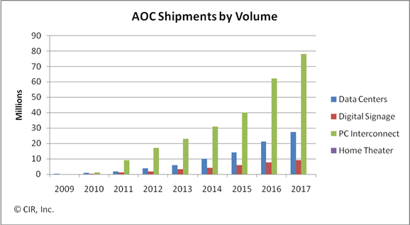
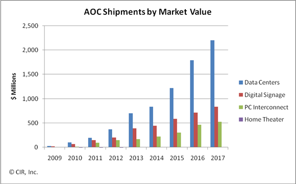
The global market for active optical cable (AOC) is forecast to grow to US $1.5bn by 2014, with the linking of datacenter equipment being the largest single market valued at $835m. Other markets for the cabling technology include digital signage, PC interconnect and home theatre.
CIR’s report entitled Active Optical Cabling: A Technology Assessment and Market Forecast notes how AOC emerged with a jolt. Two years on and the technology is now a permanent fixture that will continue to nimbly address application as they appear. This explains why CIR views AOC as an opportunistic and tactical interconnect technology.

AOC: "Opportunistic and tactical"
Loring Wirbel
What is active optical cable?
An AOC converts an electrical interface to optical for transmission across a cable before being restored to the electrical domain. Optics are embedded as part of the cabling connectors with AOC vendors using proprietary designs. Being self-contained, AOCs have the opportunity to become a retail sale at electronics speciality stores.
A common interface for AOC is the QSFP but there are AOC products that use proprietary interfaces. Indeed the same interface need not be used at each end of the cable. Loring Wirbel, author of the CIR AOC report, mentions a MergeOptics’ design that uses a 12-channel CXP interface at one end and three 4-channel QSFP interfaces at the other. “If it gets traction, everyone will want to do it,” he says.
Origins
AOC products were launched by several vendors in 2007. Start-up Luxtera saw it as an ideal entry market for its silicon photonics technology; Finisar came out with a 10Gbps serial design; while Zarlink identified AOC as a primary market opportunity, says Wirbel.
Application markets
AOC is the latest technology targeting equipment interconnect in the data centre. Typical distances linking equipment range from 10 to 100m; 10m is where 10Gbps copper cabling starts to run out of steam while 100m and above are largely tackled by structured cabling.
“Once you get beyond 100 meters, the only AOC applications I see are outdoor signage and maybe a data centre connecting to satellite operations on a campus,” says Wirbel.
AOC is used to connect servers and storage equipment using either Infiniband or Ethernet. “Keep in mind it is not so much corporate data centres as huge dedicated data centre builds from a Google or a Facebook,” says Wirbel.
AOC’s merits include its extended reach and light weight compared to copper. Servers can require metal plates to support the sheer weight of copper cabling. The technology also competes with optical pluggable transceivers and here the battleground is cost, with active optical cabling including end transceivers and the cable all-in-one.
To date AOC is used for 10Gbps links and for double data rate (DDR) and quad data rate (QDR) Infiniband. But it is the evolution of Infiniband’s roadmap - eight data rate (EDR, 20Gbps per lane) and hexadecimal data rate (HDR, 40Gbps per lane) - as well as the advent of 100m 40 and 100 Gigabit Ethernet links with their four and ten channel designs that will drive AOC demand.
The second largest market for AOC, about $450 million by 2014, and one that surprised Wirbel, is the ‘unassuming’ digital signage.
Until now such signs displaying video have been well served by 1Gbps Ethernet links but now with screens showing live high-definition feeds and four-way split screens 10Gbps feeds are becoming the baseline. Moreover distances of 100m to 1km are common.
PC interconnect is another market where AOC is set to play a role, especially with the inclusion of a high-definition multimedia interface (HDMI) interface as standard with each netbook.
“A netbook has no local storage, using the cloud instead,” says Wirbel. Uploading video from a video camera to the server or connecting video streams to a home screen via HDMI will warrant AOC, says Wirbel.
Home theatre is the fourth emerging application for AOC though Wirbel stresses this will remain a niche application.