
ECOC 2015: Reflections
Valery Tolstikhin, head of a design consultancy, Intengent

ECOC was a big show and included a number of satellite events, such as the 6th European Forum on Photonic Integration, the 3rd Optical Interconnect in Data Center Symposium and Market Focus, all of which I attended. So, lots of information to digest.
My focus was mainly on data centre optical interconnects and photonic integration.
Data centre interconnects
What became evident at ECOC is that 50 Gig modulation and the PAM-4 modulation format will be the basis of the next generation (after 100 Gig) data centre interconnect. This is in contrast to the current 100 Gig non-return-to-zero (NRZ) modulation using 25 Gig lanes.
This paves the way towards 200 Gig (4 x PAM-4 lanes at 25 Gig) and 400 Gig (4 x PAM-4 lanes at 50 Gig) as a continuation of quads of 4 x NRZ lanes at 25 Gig, the state-of-the-art data centre interconnect still to take off in terms of practical deployment.
The transition from 100 Gig to 400 Gig seems to be happening much faster than from 40Gig to 100 Gig. And 40 Gig serial finally seems to have gone; who needs 40 Gig when 50 Gig is available?
Another observation is that despite the common agreement that future new deployments should use single-mode fibre rather than multi-mode fibre, given the latter’s severe reach limitation that worsens with modulation speed, the multi-mode fibre camp does not give up easily.
That is because of the tons of multi-mode fibre interconnects already deployed, and the low cost of gallium arsenide 850 nm VCSELs these links use. However, the spectral efficiency of such interconnects is low, resulting in high multi-mode fibre count and the associated cost. This is a strong argument against such fibre.
Now, a short-wave WDM (SWDM) initiative is emerging as a partial solution to this problem, led by Finisar. Both OM3 and OM4 multi-mode fibre can be used, extending link spans to 100m at 25 Gig speeds.
Single mode fibre 4 x 25 Gig QSFP28 pluggables with a reach of up to 2 km, which a year ago were announced with some fanfare, seems to have become more of a commodity.
The SWDM Alliance was announced just before ECOC 2015, with major players like Finisar and Corning on board, suggesting this is a serious effort not to be ignored by the single mode fibre camp.
Lastly, single mode fibre 4 x 25 Gig QSFP28 pluggables with a reach of up to 2 km, which a year ago were announced with some fanfare, seems to have become more of a commodity. Two major varieties – PSM and WDM – are claimed and, probably shipping, by a growing number of vendors.
Since these are pluggables with fixed specs, the only difference from the customer viewpoint is price. That suggests a price war is looming, as happens in all massive markets. Since the current price still are an order of magnitude or more above the target $1/Gig set by Facebook and the like, there is still a long way to go, but the trend is clear.
This reminds me of that I’ve experienced in the PON market: a massive market addressed by a standardised product that can be assembled, at a certain time, using off-the-shelf components. Such a market creates intense competition where low-cost labour eventually wins over technology innovation.
Photonic integration
Two trends regarding photonic integration for telecom and datacom became clear at ECOC 2015.
One positive development is an emerging fabless ecosystem for photonic integrated circuits (PICs), or at least an understanding of a need for such. These activities are driven by silicon photonics which is based on the fabless model since its major idea is to leverage existing silicon manufacturing infrastructure. For example, Luxtera, the most visible silicon component vendor, is a fabless company.
There are also signs of the fabless ecosystem building up in the area of III-V photonics, primarily indium-phosphide based. The European JePPIX programme is one example. Here you see companies providing foundry and design house services emerging, while the programme itself supports access to PIC prototyping through multi-project wafer (MPW) runs for a limited fee. That’s how the ASIC business began 30 to 40 years ago.
A link to OEM customers is still a weak point, but I see this being fixed in the near future. Of course, Intengent, my design house company, does just that: links OEM customers and the foundries for customised photonic chip and PIC development.
As soon as PICs give a system advantage, which Infinera’s chips do, they become a system solution enabler, not merely ordinary components made a different way
The second, less positive development, is that photonic integration continues to struggle to find applications and markets where it will become a winner. Apart from devices like the 100 Gig coherent receiver, where phase control requirements are difficult to meet using discretes, there are few examples where photonic integration provides an edge.
Even a 4 x 25 Gig assembly using discrete components for today’s 100 Gig client side and data centre interconnect has been demonstrated by several vendors. It then becomes a matter of economies of scale and cheap labour, leaving little space for photonic integration to play. This is what happened in the PON market despite photonic integrated products being developed by my previous company, OneChip Photonics.
On a flip side, the example of Infinera shows where the power of photonic integration is: its ability to create more complicated PICs as needed without changing the technology.
One terabit receiver and transmitter chips developed by Infinera are examples of complex photonic circuits, simply undoable by means of an optical sub-assembly. As soon as PICs give a system advantage, which Infinera’s chips do, they become a system solution enabler, not merely ordinary components made a different way.
However, most of the photonic integration players - silicon photonics and indium phosphide alike - still try to do the same as what an optical sub-assembly can do, but more cheaply. This does not seem to be a winning strategy.
And a comment on silicon photonics. At ECOC 2015, I was pleased to see that, finally, there is a consensus that silicon photonics needs to aim at applications with a certain level of complexity if it is to provide any advantage to the customer.
Silicon photonics must look for more complex things, maybe 400 Gig or beyond, but the market is not there yet
For simpler circuits, there is little advantage using photonic integration, least of all silicon photonics-based ones. Where people disagree is what this threshold level of complexity is. Some suggest that 100 Gig optics for data centres is the starting point but I’m unsure. There are discrete optical sub-assemblies already on the market that will become only cheaper and cheaper. Silicon photonics must look for more complex things, maybe 400 Gig or beyond, but the market is not there yet.
One show highlight was the clear roadmap to 400 Gig and beyond, based on a very high modulation speed (50 Gig) and the PAM-4 modulation format, as discussed. These were supported at previous events, but never before have I seen the trend so clearly and universally accepted.
What surprised me, in a positive way, is that people have started to understand that silicon photonics does not automatically solve their problems, just because it has the word silicon in its name. Rather, it creates new challenges, cost efficiency being an important one. The conditions for cost efficient silicon photonics are yet to be found, but it is refreshing that only a few now believe that the silicon photonics can be superior by virtue of just being ‘silicon’.
I wouldn’t highlight one thing that I learned at the show. Basically, ECOC is an excellent opportunity to check on the course of technology development and people’s thoughts about it. And it is often better seen and felt on the exhibition floor than attending the conference’s technical sessions.
For the coming year, I will continue to track data centre interconnect optics, in all its flavours, and photonic integration, especially through a prism of the emerging fabless ecosystem.
Vishnu Shukla, distinguished member technical staff in Verizon’s network planning group.
There were more contributions related to software-defined networking (SDN) and multi-layer transport at ECOC. There were no new technology breakthroughs as much as many incremental evolutions to high-speed optical networking technologies like modulation, digital signal processors and filtering.
I intend to track technologies and test results related to transport layer virtualisation and similar efforts for 400 Gig-and-beyond transport.
Vladimir Kozlov, CEO and founder of LightCounting
I had not attended ECOC since 2000. It is a good event, a scaled down version of OFC but just as productive. What surprised me is how small this industry is even 15 years after the bubble. Everything is bigger in the US, including cars, homes and tradeshows. Looking at our industry on the European scale helps to grasp how small it really is.
What is the next market opportunity for optics? The data centre market is pretty clear now, but what next?
Listening to the plenary talk of Sir David Paine, it struck me how infinite technology is. It is so easy to get overexcited with the possibilities, but very few of the technological advances lead to commercial success.
The market is very selective and it takes a lot of determination to get things done. How do start-ups handle this risk? Do people get delusional with their ideas and impact on the world? I suspect that some degree of delusion is necessary to deal with the risks.
As for issues to track in the coming year, what is the next market opportunity for optics? The data centre market is pretty clear now, but what next?
US invests $610 million to spur integrated photonics
 Prof. Duncan Moore
Dubbed the American Institute for Manufacturing Integrated Photonics (AIM Photonics), the venture has attracted 124 partners includes 20 universities and over 50 companies.
The manufacturing innovation institute will be based in Rochester, New York, and will be led by the Research Foundation for the State University of New York. A key goal is that the manufacturing institute will continue after the initiative is completed in early 2021.
We are at the point in photonics where we were in electronics when we still had transistors, resistors and capacitors. What we are trying to do now is the equivalent of the electronics IC
While the focus is on photonic integrated circuits, the expectation is that the venture will end up being broader. “NASA, the Department of Energy and the Department of Defense are all interested in using this as a vehicle for doing other work,” says Duncan Moore, professor of optics at the University of Rochester.
The venture will address such issues as design, on-chip manufacturing, packaging and assembly of PICs. “We are at the point in photonics where we were in electronics when we still had transistors, resistors and capacitors,” says Moore. “What we are trying to do now is the equivalent of the electronics IC.”
"It is an amazing public-private consortium utilizing an unprecedented $610 million investment in photonics," says Richard Soref, a silicon photonics pioneer and a Group IV photonics researcher. "The large and powerful team of world-class investigators is likely to make research-and-development progress of great importance for the US and the world.”
Project plans
The first six months are being used to fill in project’s details. “There are overall budget numbers but individual projects are not well defined in the proposal,” says Moore, adding that many of the subfields - packaging, sensors and the like - will be defined and request-for-proposals issued.
An executive committee will then determine which projects are funded and to what degree. Project durations will vary from one-offs to the full five years.
The large and powerful team of world-class investigators is likely to make research-and-development progress of great importance for the US and the world
Companies backing the project include indium phosphide specialist Infinera as well as silicon photonics players Acacia Communications, Aurrion, and Intel. How the two technologies as well as Group IV photonics will be accommodated as part of the manufacturing base is still to be determined, says Prof. Moore. His expectation is that all will be investigated before a ‘shakeout’ will occur as the venture progresses.
The focus will be on telecom wavelengths and the mid-wave 3 to 5 micron band. “There are a lot of applications in that [longer] wavelength band: remote sensing, environmental analysis, and for doing things on the battlefield,” says Moore.
A public document will be issued around the year-end describing the project’s organisation.
Further information:
The White House factsheet, click here
A Photonics video interview with the chairman of the institute, Professor Robert Clark, click here
Verizon tips silicon photonics as a key systems enabler
Part 3: An operator view
Glenn Wellbrock is upbeat about silicon photonics’ prospects. Challenges remain, he says, but the industry is making progress. “Fundamentally, we believe silicon photonics is a real enabler,” he says. “It is the only way to get to the densities that we want.”
 Glenn Wellbrock
Wellbrock adds that indium phosphide-based photonic integrated circuits (PICs) can also achieve such densities.
But there are many potential silicon photonics suppliers because of its relatively low barrier to entry, unlike indium phosphide. "To date, Infinera has been the only real [indium phosphide] PIC company and they build only for their own platform,” says Wellbrock.
That an operator must delve into emerging photonics technologies may at first glance seem surprising. But Verizon needs to understand the issues and performance of such technologies. “If we understand what the component-level capabilities are, we can help drive that with requirements,” says Wellbrock. “We also have a better appreciation for what the system guys can and cannot do.”
Verizon can’t be an expert in the subject, he says, but it can certainly be involved. “To the point where we understand the timelines, the cost points, the value-add and the risk factors,” he says. “There are risk factors that we also want to understand, independent of what the system suppliers might tell us.”
The cost saving is real, but it is also the space savings and power saving that are just as important
All the silicon photonics players must add a laser in one form or another to the silicon substrate since silicon itself cannot lase, but pretty much all the other optical functions can be done on the silicon substrate, says Wellbrock: “The cost saving is real, but it is also the space savings and power saving that are just as important.”
The big achievement of silicon photonics, which Wellbrock describes as a breakthrough, is the getting rid of the gold boxes around the discrete optical components. “How do I get to the point where I don’t have fibre connecting all these discrete components, where the traces are built into the silicon, the modulator is built in, even the detector is built right in.” The resulting design is then easier to package. “Eventually I get to the point where the packaging is glass over the top of that.”
So what has silicon photonics demonstrated that gives Verizon confidence about its prospects?
Wellbrock points to several achievements, the first being Infinera’s PICs. Yes, he says, Infinera’s designs are indium phosphide-based and not silicon photonics, but the company makes really dense, low-power and highly reliable components.
He also cites Cisco’s silicon photonics-based CPAK 100 Gig optical modules, and Acacia, which is applying silicon photonics and its in-house DSP-ASICs to get a lower power consumption than other, high-end line-side transmitters.
Verizon believes the technology will also be used in CFP4 and QSFP28 optical modules, and at the next level of integration that avoids pluggable modules on the equipment's faceplate altogether.
But challenges remain. Scale is one issue that concerns Verizon. What makes silicon chips cheap is the fact that they are made in high volumes. “It [silicon photonics] couldn’t survive on just the 100 gigabit modules that the telecom world are buying,” says Wellbrock.
If these issues are not resolved, then indium phosphide continues to win for a long time because that is where the volumes are today
When Verizon asks the silicon photonics players about how such scale will be achieved, the response it gets is data centre interconnect. “Inside the data centre, the optics is growing so rapidly," says Wellbrock. "We can leverage that in telecom."
The other issue is device packaging, for silicon photonics and for indium phosphide. It is ok making a silicon-photonics die cheaply but unless the packaging costs can be reduced, the overall cost saving is lost. ”How to make it reliable and mainstream so that everyone is using the same packaging to get cost down,” says Wellbrock.
All these issues - volumes, packaging, increasing the number of applications a single part can be applied to - need to be resolved and almost simultaneously. Otherwise, the technology will not realise its full potential and the start-ups will dwindle before the problems are fixed.
“If these issues are not resolved, then indium phosphide continues to win for a long time because that is where the volumes are today,” he says.
Verizon, however, is optimistic. “We are making enough progress here to where it should all pan out,” says Wellbrock.
Silicon photonics economics set to benefit III-V photonics
Silicon photonics promises to deliver cheaper optical components using equipment, processes and fabrication plants paid for by the chip industry. Now, it turns out, traditional optical component players using indium phosphide and gallium arsenide can benefit from similar economies, thanks to the wireless IC chip industry.
 Valery TolstikhinSilicon photonics did a good thing; it turned the interest of the photonics industry to the operational ways of silicon
So argues Valery Tolstikhin, head of a design consultancy, Intengent, and former founder and CTO of Canadian start-up OneChip Photonics. The expectations for silicon photonics may yet to be fulfilled, says Tolstikhin, but what the technology has done is spark interest in the economics of component making. And when it comes to chip economics, volumes count.
“For III-V photonics - indium phosphide and related materials - you have all kinds of solutions, designs and processes, but all are boutique,” says Tolstikhin. “They are not commercialised in a proper way and there is no industrial scale.” The reason for this is simple: optical components is a low-volume industry.
This is what Tolstikhin seeks to address by piggybacking on high-volume indium phosphide and gallium arsenide fabrication plants that make monolithic microwave integrated circuits (MMICs) for wireless.
“To take photonics out of boutique fabs, you need to do some standardisation and move to a fabless model, then you can load the fabs day and night with wafers,” says Tolstikhin. “That is the only way to make a process mature, reproducible and reliable.”
Tolstikhin has spent the last decade pursuing this approach. “The idea is to use something available in indium phosphide which is relatively close to a pure-play foundry.” A pure-play foundry is a fab that makes chips but does not design, market or sell them as its own products.
Tolstikhin’s first involvement was at start-up OneChip Photonics which developed an indium-phosphide platform that used a variety of photonic devices to make photonic integrated circuits (PICs), based on a commercial MMIC process.
The issue with III-V integrated photonics is that to implement different functions - a passive waveguide and a laser, for example - different materials are needed. “What makes a low-loss passive waveguide, does not work for the laser,” says Tolstikhin.
To overcome this, the wafer is repeatedly etched in certain areas, to remove unwanted material, and new layers grown instead with the required material, a process known as selective-area etch and regrowth. This is a complicated and relatively low-yield process that is custom to companies and their fabs, he says: “This is how all commercial lasers and PICs are made.”
In contrast, MMICs using indium phosphide do not need regrowth, simplifying the process considerably. To use a MMIC fab for an optical design, however, it must be developed in a way that avoids the need for regrowth stages.
“At OneChip we believe we did the first commercial laser - not just the laser but the PIC with it - regrowth-free,” says Tolstikhin. “It was made in a MMIC fab, that is the key.”
“To take photonics out of boutique fabs, you need to do some standardisation and move to a fabless model, then you can load the fabs day and night with wafers”
Wafer economics
To understand the relative economics, Tolstikhin compares the number of wafers - wafer starts - processed in silicon, indium phosphide and gallium arsenide.
One large TSMC fab has 400,000 12-inch CMOS wafer starts a year whereas globally the figure is equivalent to some 70 million such wafers a year. For MMICs, one fab Tolstikhin works with has 15,000 4-inch indium phosphide wafer starts a year whereas a large optical component company uses just a couple of thousand 3-inch indium phosphide wafers a year.
“In photonics, the [global] volumes – even for components going into the most massive markets like PON and the data centre interconnects – are still very low,” says Tolstikhin.
Gallium arsenide is somewhere in between: Win’s fab in Taiwan, which makes power amplifiers for wireless and other MMICs, has 250,000 6-inch wafers starts a year, while TriQuint’s fab in USA, with similar product line in wireless, totals 150,000 6-inch wafer starts a year.
Such volumes are not negligible and exceed all the needs of photonics, he says, enabling photonics to make claims similar to those trumpeted for silicon photonics: a mature process with a well-established quality system and, with its volumes, delivers better economics.
Moreover, if applications that currently are based on indium phosphide could be transferred to gallium arsenide, that would give an order of magnitude economies of scale, says Tolstikhin: “One example is mid-reach single-mode optical interconnects with an operating wavelength around 1060 nm, with gallium arsenide used for the transmitter, receiver and transceiver PICs”.
And while the scale of III-V semiconductor manufacturing may still be much lower than CMOS, the up-front cost involved in using a III-V fab is also much less.
Using III-V semiconductors for analogue electronics like the laser /modulator drivers or the trans-impedance amplifier also delivers a speed advantage: heterojunction bipolar transistors (HBTs) in indium phosphide have been demonstrated working at up to 400 GHz, and these, being vertical devices, do not have their speed scaled with lithography. In contrast, CMOS analog electronics is much slower and its device speed is scalable with lithography resolution. A 130 nm CMOS process, the starting point for silicon photonics, cannot support optical components with bit rates beyond 10 Gbps.
Design house
Intengent, Tolstikhin’s company, acts as a bridge between OEMs building optical components and sub-systems and the III-V foundries making photonic chips for them.
He compares Intengent to what application-specific IC (ASIC) companies used to do for the electronic chip industry. Intengent works with the OEM to specify and design the photonic chip based on its system application and then works with the fab to develop and turn the chip into a product by meeting its design rules and process capabilities.
“The aim is that you can go and design within existing fabs and processes something that meets the customer’s application and requirements,” he says.
Tolstikhin is also working with ELPHiC, a Canadian start-up that is raising funding to develop single-mode mid-board optics. The indium-phosphide design combines analogue electronic circuitry with the photonics.
“It appears the best way [to do mid-board optics] is based on electronic and photonic integration onto one substrate and indium phosphide is a natural choice for such a substrate,” he says.
Tolstikhin makes clear he is not against silicon photonics. “It did a good thing; it turned the interest of the photonics industry to the operational ways of silicon: standardised processes, pure-play foundries, device designs separate from the semiconductor physics, and circuit designs separate from the wafer processing.”
As a result, something similar is now being pursued in III-V photonics.
MACOM acquires Mindspeed to boost 100 Gig offerings
 Ray MoroneyThe Mindspeed acquisition increases the serviceable addressible market for MACOM, both geographical - the company will strengthen its presence in Asia Pacific - and by gaining new equipment vendor accounts. It also broadens MACOM's 100 Gigabit physical device portfolio.
"We are targeting the 100 Gig buildout and the growth coming from that," says Ray Moroney, product line manager, opto-device business unit at MACOM.
Mindpeed also makes a broad portfolio of crosspoint switches used in datacom equipment, and several families of communications processors.
With the acquisition of Mindspeed we have the full electronics bill-of-materials for CFP2 and CFP4 [module] client-side applications
MACOM entered opto-electronics with the acquisition of Optimai in 2011 that had long-haul and client-side modulator drivers and trans-impedance amplifiers (TIAs). Now with Mindspeed's products, MACOM can capture client-side designs with clock data recovery chips and quad-channel TIAs for 100 Gig modules. "With the acquisition of Mindspeed we have the full electronics bill-of-materials for CFP2 and CFP4 [module] client-side applications," says Moroney.
MACOM also gains silicon germanium technology alongside its indium phosphide and gallium arsenide technologies. Silicon germanium has a lower cost structure once a design is being made in volume production, says Moroney, but the R&D and mask costs are generally higher. Silicon germanium also allows significant integration. "It is BiCMOS in nature," says Moroney. "You can integrate full CMOS functionality into a design too." For example digital control can be added alongside analogue functions. Moroney says the company will use silicon germanium for high-performance analogue designs like TIAs as well as high-frequency millimeter wave and microwave applications.
The company is considering its options regarding the future of the communications processors arm of Mindspeed's business. "MACOM is very much an analogue/ RF company," says Moroney. "It [communications processors] is certainly not seen as a core area of investment for MACOM."
Mellanox to acquire silicon photonics player Kotura
 Source: Gazettabyte
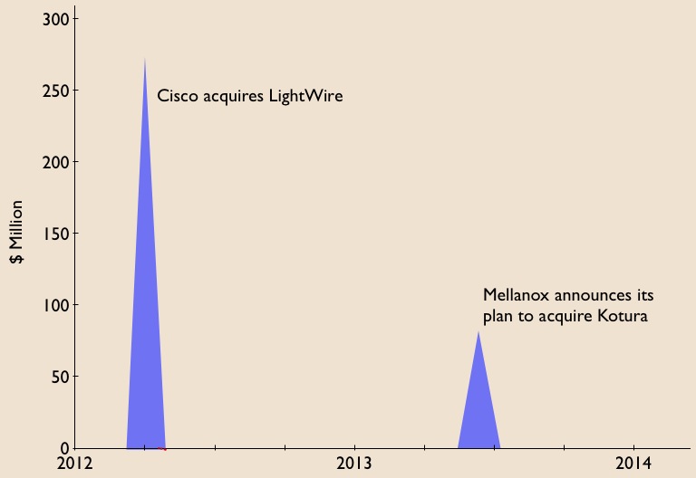
Mellanox Technologies has announced its intention to acquire silicon photonics player, Kotura, for $82 million.
The acquisition will enable Mellanox to deliver 100 Gigabit Infiniband and Ethernet interconnect in the coming two years. lt will also provide Kotura with the resources needed to bring its 100 Gigabit QSFP to market. Mellanox will also gain Kotura's optical engine for use in active optical cables and new mid-plane platform designs, as well as future higher speed interfaces.
The news is also significant for the optical component industry. Kotura is one of the three established merchant silicon photonics players - the others being LightWire and Luxtera - that have spent years developing their technologies.
LightWire was acquired by Cisco Systems in March 2012 for US $271 million and now Mellanox plans to acquire Kotura. The two equipment vendors recognise the value of the technology, bringing it in-house to reduce system interconnect costs and as a long term differentiator for their equipment and ASIC designs. Mellanox, as a silicon photonics player, will compete with Intel, with its own silicon photonics technology, and Cisco Systems.
Kotura has been using its technology to sell telecom products such as variable optical attenuators and multiplexers. The start-up recently announced its 100 Gig QSFP that uses wavelength division multiplexing (WDM) transmitter and receiver chips. The product is to become available in 2014.
In an interview last year, Kotura's CTO, Mehdi Asghari, discussed a roadmap showing how its 100 Gigabit silicon photonics technology could scale to 400 Gigabit and eventually 1.6 Terabit.
"Our devices are capable of running at 40 or 50 Gigabit-per-second (Gbps), depending on the electronics. The electronics is going to limit the speed of our devices. We can very easily see going from four channels at 25Gbps to 16 channels at 25Gbps to provide a 400 Gigabit solution," Asghari told Gazettabyte.
Kotura also discussed how the line rate could be increased to 50Gbps either using a non-return-to-zero (NRZ) line rate or using a multi-level modulation such as pulse amplitude modulation (PAM).
"To get to 1.6 Terabit transceivers, we envisage something running at 40Gbps times 40 channels or 50Gbps times 32 channels. We already have done a single receiver chip demonstrator that has 40 channels, each at 40Gbps," said Asghari.
"These things in silicon are not a big deal. The III-V guys really struggle with yield and cost. But you can envisage scaling to that level of complexity in a silicon platform."
Silicon photonics will not replace existing VCSEL or indium phosphide-based transceiver designs. But there is no doubting silicon photonics is emerging as a key optical technology and the segment is heating up.
If the early start-ups are being acquired, there have been more recent silicon photonics players entering the marketplace such as Aurrion, Skorpios Technologies and Teraxion. There are also internal developments among equipment players such as Alcatel-Lucent, HP Labs and IBM. Indeed Kotura has worked closely with Oracle (Sun Microsystems)
Further acquisitions of silicon photonic players should be expected as companies start designing next generation, denser systems and adopt 100 Gigabit and faster interfaces.
Equally, established optical component and module companies will likely enter quietly (and not so quietly) the marketplace adding silicon photonics to their technology toolkits when the timing is right.
Trends to watch
Two industry trends are underway regarding silicon photonics.
The first is system vendors wanting to own the technology to reduce their costs while recognising a need to control and understand the technology as they tackle more complex equipment designs.
The other, what at first glance is a contrarian trend, is the democratisation of silicon photonics.
The technology is slowly passing from the select few to become more generally available for industry use. For this to happen, the relevant design tools need to mature as do third-party fabrication plants that will manufacture the silicon photonics designs.
Appendix:
On June 4th, 2013, Mellanox announced a definitive agreement to acquire chip company IPtronics for $47.5 million as it builds out its in-house technologies for optical interconnect. Click here
Futher reading:
Avago to acquire CyOptics, click here
OIF promotes uni-fabric switches & 100G transmitter
 The OIF's OTN implementation agreement (IA) allows a packet fabric to also switch OTN traffic. The result is that operators can now use one switch for both traffic types, aiding IP/ Ethernet and OTN convergence. Source: OIF
Improving the switching capabilities of telecom platforms without redesigning the switch as well as tinier 100 Gigabit transmitters are just two recent initiatives of the Optical Internetworking Forum (OIF).
The OIF, the industry body tackling design issues not addressed by the IEEE and International Telecommunication Union (ITU) standards bodies, has just completed its OTN-over-Packet-Fabric protocol that enables optical transport network (OTN) traffic to be carried over a packet switch. The protocol works by modifying the line cards at the switch's input and output, leaving the switch itself untouched (see diagram above).
In contrast, the OIF is starting a 100 Gigabit-per-second (Gbps) transmitter design project dubbed the integrated dual-polarisation quadrature modulated transmitter assembly (ITXA). The Working Group aims to expand the 100Gbps applications with a transmitter design half the size of the OIF's existing 100Gbps transmitter module.
The Working Group also wants greater involvement from the system vendors to ensure the resulting 100 Gig design is not conservative. "We joke about three types of people that attend these [working group] meetings," says Karl Gass, the OIF’s Physical and Link Layer Working Group vice-chair. "The first group has something they want to get done, the second group has something already and they don't want something to get done, and the third group want to watch." Quite often it is the system vendors that fall into this third group, he says.
OTN-over-Packet-Fabric protocol
The OTN protocol enable a single switch fabric to be used for both traffic types - packets and time-division multiplexed (TDM) OTN - to save cost for the operators.
"OTN is out there while Ethernet is prevalent," says Winston Mok, technical author of the OTN implementation agreement. "What we would like to do is enable boxes to be built that can do both economically."
 The existing arrangement where separate packet and OTN time-division multiplexing (TDM) switches are required. Source: OIF
Platforms using the protocol are coming to market. ECI Telecom says its recently announced Apollo family is one of the first OTN platforms to use the technique.
The protocol works by segmenting OTN traffic into a packet format that is then switched before being reconstructed at the output line card. To do this, the constant bit-rate OTN traffic is chopped up so that it can easily go through the switch as a packet. "We want to keep the [switch] fabric agnostic to this operation," says Mok. "Only the line cards need to do the adaptations."
The OTN traffic also has timing information which the protocol must convey as it passes through the switch. The OIF's solution is to vary the size of the chopped-up OTN packets. The packet is nominally 128-bytes long. But the size will occasionally be varied to 127 and 126 bytes as required. These sequences are interpreted at the output of the switch as rate information and used to control a phase-locked loop.
Mok says the implementation agreement document that describes the protocol is now available. The protocol does not define the physical layer interface connecting the line card to the switch, however. "Most people have their own physical layer," says Mok.
100 Gig ITXA
The ITXA project will add to the OIF's existing integrated transmitter document. The original document addresses the 100 Gigabit transmitter for dual-polarisation, quadrature phase-shift keying (DP-QPSK) for long-haul optical transmission. The OIF has also defined 100Gbps receiver assembly and tunable laser documents.
The latest ITXA Working Group has two goals: to shrink the size of the assembly to lower cost and increase the number of 100Gbps interfaces on a line card, and to expand the applications to include metro. The ITXA will still address 100Gbps coherent designs but will not be confined to DP-QPSK, says Gass.
"We started out with a 7x5-inch module and now there is interest from system vendors and module makers to go to smaller [optical module] form factors," says Gass. "There is also interest from other modulator vendors that want in on the game."
The reduce size, the ITXA will support other modulator technologies besides lithium niobate that is used for long-haul. These include indium phosphide, gallium arsenide and polymer-based modulators.
Gass stresses that the ITXA is not a replacement for the current transmitter implementation. "We are not going to get the 'quality' that we need for long-haul applications out of other modulator technologies," he says. "This is not a Gen II [design].
The Working Group's aim is to determine the 'greatest common denominator' for this component. "We are trying to get the smallest form factor possible that several vendors can agree on," says Gass. "To come out with a common pin out, common control, common RF (radio frequency) interface, things like that."
Gass says the work directions are still open for consideration. For example, adding the laser with the modulator. "We can come up with a higher level of integration if we consider adding the laser, to have a more integrated transmitter module," says Gass.
As for wanting great system-vendor input, the Working Group wants more of their system-requirement insights to avoid the design becoming too restrictive.
"You end up with component vendors that do all the work and they want to be conservative," says Gass. "The component vendors don't want to push the boundaries as they want to hit the widest possible customer base."
Gass expects the ITXA work to take a year, with system demonstrations starting around mid-2013.