Optical interconnect specialist Ayar Labs has announced that it is working with Nvidia, a leader in artificial intelligence (AI) and machine learning silicon, systems and software.
In February Ayar Labs announced a strategic collaboration with the world’s leading high-performance computing (HPC) firm, Hewlett Packard Enterprise (HPE).
Both Nvidia and HPE were part of the Series C funding worth $130 million that Ayar Labs secured in April.
Work partnerships
Ayar Labs has chiplet and external laser source technologies that enable optical input-output (I/O) suited for AI and high-performance computing markets.
Charles Wuischpard, CEO of Ayar Labs, says the work with HPE and Nvidia share common characteristics.
HPE is interested in optical interfaces for high-performance computing fabrics and, in particular, future generations of its Slingshot technology.
Nvidia is also interested in fabrics with its Mellanox technology, but its chips also impact the server. Wuishchpard describes its work with Nvidia as optically enabling Nvidia’s NVLink, its graphics processing unit (GPU) interface.
Nvidia’s optical needs
Bill Dally, chief scientist and senior vice president of research at Nvidia, outlined the company’s interest in optical interconnect at the OFC conference, held in San Diego in March.
Dally started by quantifying the hierarchy of bandwidths and power requirements when sending a bit in computing systems.
The maximum bandwidth and lowest power needs occur, not surprisingly, when data is sent on-chip, between the chip’s processing elements.
With each hierarchical connection jump after that – between chips on an interposer hosting, for example, GPUs and memory (referred to as a module), between modules hosted on a printed circuit board (PCB), linking the boards in a cabinet, and connecting cabinets in a cluster – the bandwidth drops (dubbed bandwidth tapering) and more power is needed to transmit a bit.
There are also different technologies used for the jumps: electrical traces connect the modules on the PCB; electrical cables link the boards in a cabinet (1m to 3m), while active optical cables link the cabinets (5m to 100m).
One issue is that electrical signalling is no longer getting faster (the FO4 delay metric is now constant) with each new CMOS process node. Another issue is that the electrical reach is shrinking with each signalling speed hike: 50-gigabit signals can span 3m, while 200-gigabit signals can span 1m.
Co-packaged optics, where optics are placed next to the IC, promises the best of both worlds: bettering the metrics of PCBs and electrical cable while matching the reach of active optical cables.
Co-packaged optics promises a 5x saving in power when sending a bit compared to a PCB trace while costing a tenth of an active optical cable yet matching its 100m reach. Co-packaged optics also promises a fourfold increase in density (bit/s/mm) compared to PCB traces, says Nvidia.
However, meeting these targets requires overcoming several challenges.
One is generating efficient lasers that deliver aligned frequency grids. Another is getting the micro-ring resonators, used for modulating the data over WDM links, to work reliably and in volume. Nvidia plans to use 8 or 16 micro-ring resonators per WDM link and has developed five generations of test chips that it is still evaluating.
Another issue is packaging the optics, reducing the optical loss when coupling the fibre to the GPU while avoiding the need for active alignment. Cost is a big unknown, says Dally, and if co-packaged optics proves significantly more costly than an electrical cable, it will be a non-starter.
Nvidia outlined an example optical link using 8- or 16-channel WDM links, each channel at 25 gigabit-per-second (Gbps), to enable 200 and 400-gigabit optical links.
Using two polarisations, 800-gigabit links are possible while upgrading each lambda to 50Gbps, and link speed doubles again to 1.6 terabits.
Implementing such links while meeting the cost, power, density and reach requirements is why Nvidia has invested in and is working with Ayar Labs.
“Nvidia has been keeping an eye on us for some time, and they are generally big believers in a micro-ring WDM-based architecture with a remote light source,” says Wuishchpard.
Nvidia is optimistic about overcoming the challenges and that in the coming years – it won’t say how many – it expects electrical signalling to be used only for power. At the same time, co-packaged optics will handle the interconnect.
Nvidia detailed a conceptual GPU architecture using co-packaged optics.
Each GPU would be co-packaged with two optical engines, and two GPUs would sit on a card. Eight or nine cards would fill a chassis and eight to 10 chassis a cabinet.
Each GPU cabinet would then connect to a switch cabinet which would host multiple switch chips, each switch IC co-packaged with six optical engines.
The resulting cluster would have 4,000 to 8,000 GPUs, delivering a ‘flat bandwidth taper’.
HPE’s roadmap
Ayar Labs is collaborating with HPE to develop optical interconnect technology for high-performance computing while jointly developing an ecosystem for the technology.
Marten Terpstra
“This is not just a component that you stick on, and your product becomes better and cheaper,” says Marten Terpstra, senior director of product management and high-performance networks at HPE. “This is a change in architecture.”
HPE is interested in Ayar Labs’ optical interconnect chiplets and lasers for upcoming generations of its Slingshot interconnect technology used for its ‘Shasta ‘ HPE Cray EX and other platforms.
The increase in signalling speeds from 50 to 100 gigabits and soon 200 gigabits is making the design of products more complicated and expensive in terms of cost, power and cooling.
“This [optical interconnect] is something you need to prepare for several years in advance,” says Terpstra. “It is a shift in how you create connectivity, an architectural change that takes time.”
Shasta architecture
HPE’s Slingshot interconnect is part of the liquid-cooled Shasta and a top-of-rack switch for air-cooled HPE Cray supercomputers and HPC clusters.
“There are two parts to Slingshot: the Rosetta chipset which sits inside the switch, and the Cassini chipset which sits inside a NIC [network interface controller] on the compute nodes,” says Terpstra.
The Shasta architecture supports up to 279,000 nodes, and any two endpoints can talk to each with a maximum of three hops.
The Shasta platform is designed to have a 10-year lifespan and has been built to support several generations of signalling.
The Rosetta is a 12.8Tbps (64x200Gbps) switch chipset. Terpstra points out that the topology of the switching in high-performance computing differs from that found in the data centre, such that the switch chip needs upgrading less frequently.
Shasta uses a dragonfly topology which is more distributed, whereas, in the data centre, the main aggregation layer distributes tremendous amounts of end-point traffic.
HPE is working on upgrading the Slingshot architecture but says endpoint connectivity is not growing as fast as the connectivity between the switches.
“We are driven by the capabilities of PCI Express (PCIe) and CXL and how fast you can get data in and out of the different endpoints,” says Terpstra. “The connectivity to the endpoints is currently 200 gigabits, and it will go to 400 and 800 gigabits.”
PCIe 6.0 is still a few years out, and it will support about 800 gigabits.
“The network as we know it today – or the fabric – is our current means by which we connect endpoints,” says Terpstra. “But that definition of endpoints is slowly morphing over time.”
A traditional endpoint compromises a CPU, GPU and memory, and there is a transition between the buses or interfaces such as PCIe, HDMI or NVLink to such networking protocols as Ethernet or Infiniband.
“That transition between what is inside and what is outside a compute node, and the networking that sits in between, that will become way more grey in the next few generations,” says Terpstra.
HPE’s interest in Ayar Labs’ optical interconnect technology is for both Slingshot and disaggregated architectures, the connectivity to the endpoint and the types of disaggregated endpoints built. So, for example, linking GPUs, linking CPUs, and also GPU-to-memory connections.
And just as with Nvidia’s designs, such connections have limitations in power, distance and cost.
“This kind of [optical input-output] technology allows you to overcome some of these limitations,” says Terpstra. “And that will become a part of how we construct these systems in the next few years.”
Ayar Labs’ work with both Nvidia and HPE has been ongoing since the year-start.
Funding
How will Ayar Labs be using the latest funding?
“Well, I can make payroll,” quips Wuischpard.
The funding will help staff recruitment; the company expects to have 130 staff by year-end. It will also help with manufacturing and issues such as quality and testing.
The start-up has orders this year to deliver thousands of units that meet certain specification and quality levels. “Samples to thousands of units is probably harder than going from thousands to tens of thousands of units,” says Wuischpard.
The company also has other partnerships in the pipeline, says Wuischpard, that it will announce in future.
Near package optics has emerged as companies have encountered the complexities of co-packaged optics. It should not be viewed as an alternative to co-packaged optics but rather a pragmatic approach for its implementation.
Co-packaged optics will be one of several hot topics at the upcoming OFC show in March.
Placing optics next to silicon is seen as the only way to meet the future input-output (I/O) requirements of ICs such as Ethernet switches and high-end processors.
For now, pluggable optics do the job of routing traffic between Ethernet switch chips in the data centre. The pluggable modules sit on the switch platform’s front panel at the edge of the printed circuit board (PCB) hosting the switch chip.
But with switch silicon capacity doubling every two years, engineers are being challenged to get data into and out of the chip while ensuring power consumption does not rise.
One way to boost I/O and reduce power is to use on-board optics, bringing the optics onto the PCB nearer the switch chip to shorten the electrical traces linking the two.
The Consortium of On-Board Optics (COBO), set up in 2015, has developed specifications to ensure interoperability between on-board optics products from different vendors.
However, the industry has favoured a shorter still link distance, coupling the optics and ASIC in one package. Such co-packaging is tricky which explains why yet another approach has emerged: near package optics.
I/O bottleneck
“Everyone is looking for tighter and tighter integration between a switch ASIC, or ‘XPU’ chip, and the optics,” says Brad Booth, president at COBO and principal engineer, Azure hardware architecture at Microsoft. XPU is the generic term for an IC such as a CPU, a graphics processing unit (GPU) or even a data processing unit (DPU).
What kick-started interest in co-packaged optics was the desire to reduce power consumption and cost, says Booth. These remain important considerations but the biggest concern is getting sufficient bandwidth on and off these chips.
“The volume of high-speed signalling is constrained by the beachfront available to us,” he says.
Booth cites the example of a 16-lane PCI Express bus that requires 64 electrical traces for data alone, not including the power and ground signalling. “I can do that with two fibres,” says Booth.
Nhat Nguyen
Near package optics
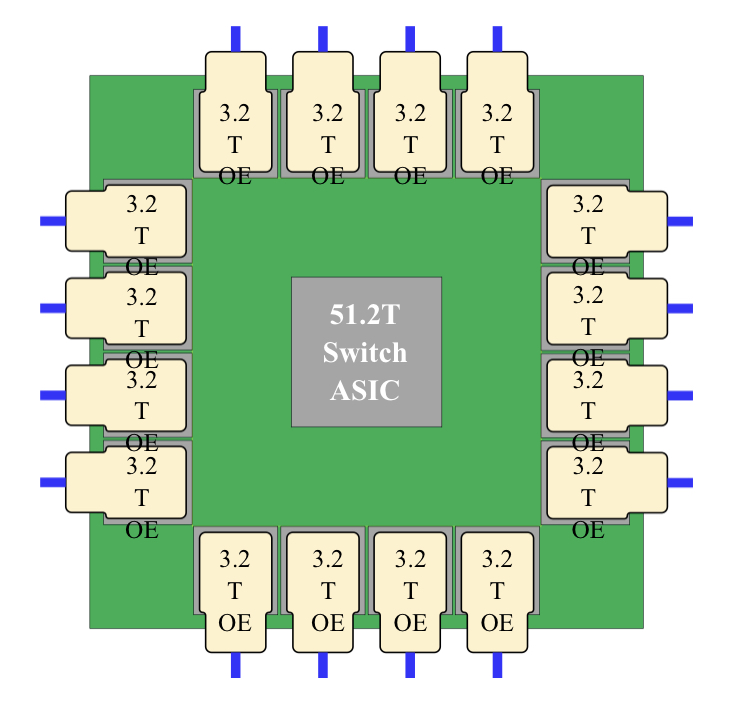
With co-packaged optics, the switch chip is typically surrounded by 16 optical modules, all placed on an organic substrate (see diagram below).
“Another name for it is a multi-chip module,” says Nhat Nguyen, senior director, solutions architecture at optical I/O specialist, Ayar Labs.
A 25.6-terabit Ethernet switch chip requires 16, 1.6 terabits-per-second (1.6Tbps) optical modules while upcoming 51.2-terabit switch chips will use 3.2Tbps modules.
“The issue is that the multi-chip module can only be so large,” says Nguyen. “It is challenging with today’s technology to surround the 51.2-terabit ASIC with 16 optical modules.”
A 51.2-terabit Ethernet switch chip surrounded by 16, 3.2Tbps optical modules. Source: OIF.
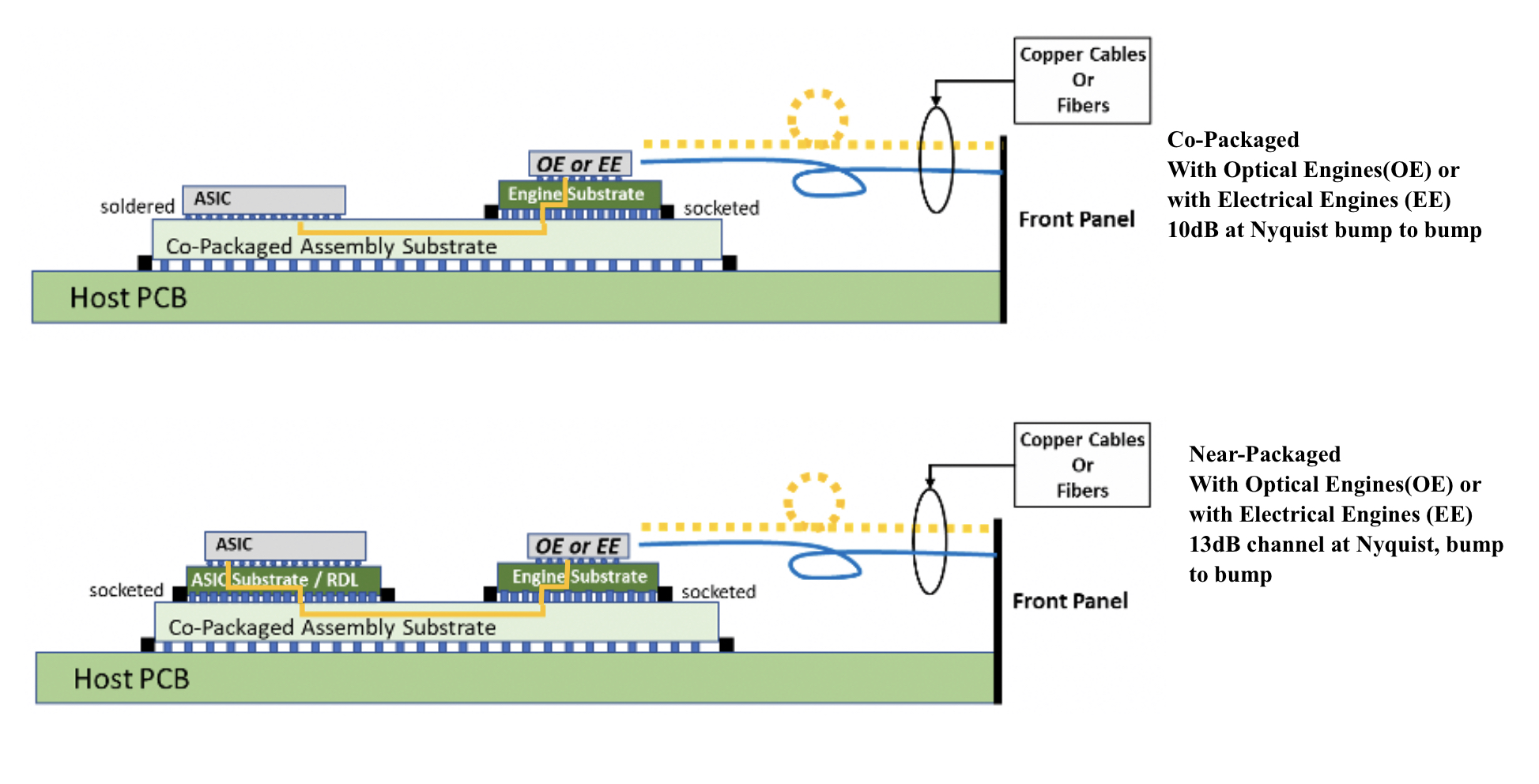
Near package optics tackles this by using a high-performance PCB substrate – an interposer – that sits on the host board, in contrast to co-packaged optics where the modules surround the chip on a multi-chip module substrate.
The near package optics’ interposer is more spacious, making the signal routing between the chip and optical modules easier while still meeting signal integrity requirements. Using the interposer means the whole PCB doesn’t need upgrading which would be extremely costly.
Some co-packaged optics design will use components from multiple suppliers. One concern is how to service a failed optical engine when testing the design before deployment. “That is one reason why a connector-based solution is being proposed,” says Booth. “And that also impacts the size of the substrate.”
A larger substrate is also needed to support both electrical and optical interfaces from the switch chip.
Platforms will not become all-optical immediately and direct-attached copper cabling will continue to be used in the data centre. However, the issue with electrical signalling, as mentioned, is it needs more space than fibre.
“We are in a transitional phase: we are not 100 per cent optics, we are not 100 per cent electrical anymore,” says Booth. “How do you make that transition and still build these systems?”
Perspectives
Ayar Labs views near package optics as akin to COBO. “It’s an attempt to bring COBO much closer to the ASIC,” says Hugo Saleh, senior vice president of commercial operations and managing director of Ayar Labs U.K.
However, COBO’s president, Booth, stresses that near package optics is different from COBO’s on-board optics work.
“The big difference is that COBO uses a PCB motherboard to do the connection whereas near package optics uses a substrate,” he says. “It is closer than where COBO can go.”
It means that with near package optics, there is no high-speed data bandwidth going through the PCB.
Booth says near package optics came about once it became obvious that the latest 51.2-terabit designs – the silicon, optics and the interfaces between them – cannot fit on even the largest organic substrates.
“It was beyond the current manufacturing capabilities,” says Booth. “That was the feedback that came back to Microsoft and Facebook (Meta) as part of our Joint Development Foundation.”
Near package optics is thus a pragmatic solution to an engineering challenge, says Booth. The larger substrate remains a form of co-packaging but it has been given a distinct name to highlight that it is different to the early-version approach.
Nathan Tracy, TE Connectivity and the OIF’s vice president of marketing, admits he is frustrated that the industry is using two terms since co-packaged optics and near package optics achieve the same thing. “It’s just a slight difference in implementation,” says Tracy.
COBO is another organisation working on specifications for co-packaged optics, focussing on connectivity issues.
The two design approaches: co-packaged optics and near package optics. Source: OIF.
Technical differences
Ayar Labs highlights the power penalty using near package optics due to its use of longer channel lengths.
For near package optics, lengths between the ASIC and optics can be up to 150mm with the channel loss constrained to 13dB. This is why the OIF is developing the XSR+ electrical interface, to expand the XSR’s reach for near package optics.
In contrast, co-packaged optics confines the modules and host ASIC to 50mm of each other. “The channel loss here is limited to 10dB,” says Nguyen. Co-packaged optics has a lower power consumption because of the shorter spans and 3dB saving.
Ayar Labs highlights its optical engine technology, the TeraPHY chiplet that combines silicon photonics and electronics in one die. The optical module surrounding the ASIC in a co-packaged design typically comprises three chips: the DSP, electrical interface and photonics.
“We can place the chiplet very close to the ASIC,” says Nguyen. The distance between the ASIC and the chiplet can be as close as 3-5mm. Whether on the same interposer Ayar Labs refers to such a design using athird term: in-package optics.
Ayar Labs says its chiplet can also be used for optical modules as part of a co-packaged design.
The very short distances using the chiplet result in a power efficiency of 5pJ/bit whereas that of an optical module is 15pJ/bit. Using TeraPHY for an optical module co-packaged design, the power efficiency is some 7.5pJ/bit, half that of a 3-chip module.
A 3-5mm distance also reduces the latency while the bandwidth density of the chiplet, measured in Gigabit/s/mm, is higher than the optical module.
Co-existence
Booth refers to near package optics as ‘CPO Gen-1’, the first generation of co-packaged optics.
“In essence, you have got to use technologies you have in hand to be able to build something,” says Booth. “Especially in the timeline that we want to demonstrate the technology.”
Is Microsoft backing near package optics?
Hugo Saleh
“We are definitely saying yes if this is what it takes to get the first level of specifications developed,” says Booth.
But that does not mean the first products will be exclusively near package optics.
“Both will be available and around the same time,” says Booth. “There will be near packaged optics solutions that will be multi-vendor and there will be more vertically-integrated designs; like Broadcom, Intel and others can do.”
From an end-user perspective, a multi-vendor capability is desirable, says Booth.
Ayar Labs’ Saleh sees two developing paths.
The first is optical I/O to connect chips in a mesh or as part of memory semantic designs used for high-performance computing and machine learning. Here, the highest bandwidth and lowest power are key design goals.
Ayar Labs has just announced a strategic partnership with high performance computing leader, HPE, to design future silicon photonics solutions for HPE’s Slingshot interconnect that is used for upcoming Exascale supercomputers and also in the data centre.
The second path concerns Ethernet switch chips and here Saleh expects both solutions to co-exist: near package optics will be an interim solution with co-packaged optics dominating longer term. “This will move more slowly as there needs to be interoperability and a wide set of suppliers,” says Saleh.
Booth expects continual design improvements to co-packaged optics. Further out, 2.5D and 3D chip packaging techniques, where silicon is stacked vertically, to be used as part of co-packaged optics designs, he says.
Gazettabyte is asking industry figures for their thoughts after attending the recent ECOC show, held in Dublin. In particular, what developments and trends they noted, what they learned and what, if anything, surprised them. Here are the first responses from Huawei, OFS Fitel and ADVA.
James Wangyin, senior product expert, access and transmission product line at Huawei
At ECOC, one technology that is becoming a hot topic is machine learning. There is much work going on to model devices and perform optimisation at the system level.
And while there was much discussion about 400-gigabit and 800-gigabit coherent optical transmissions, 200-gigabit will continue to be the mainstream speed for the coming three-to-five years.
That is because, despite the high-speed ports, most networks are not being run at the highest speed. More time is also needed for 400-gigabit interfaces to mature before massive deployment starts.
BT and China Telecom both showed excellent results running 200-gigabit transmissions in their networks for distances over 1,000km.
We are seeing this with our shipments; we are experiencing a threefold year-on-year growth in 200-gigabit ports.
Another topic confirmed at ECOC is that fibre is a must for 5G. People previously expressed concern that 5G would shrink the investment of fibre but many carriers and vendors now agree that 5G will boost the need for fibre networks.
As for surprises at the show, the main discussion seems to have shifted from high-speed optics to system-level or device-level optimisation using machine learning.
Many people are also exploring new applications based on the fibre network.
For example, at a workshop to discuss new applications beyond 5G, a speaker from Orange talked about extending fibre connections to each room, and even to desktops and other devices. Other operators and systems vendors expressed similar ideas.
Verizon discussed, in another market focus talk, its monitoring of traffic and the speed of cars using fibre deployed alongside roads. This is quite impressive.
We are also seeing the trend of using fibre and 5G to create a fully-connected world.
Such applications will likely bring new opportunities to the optical industry.
Two other items to note.
The Next Generation Optical Transport Network Forum (NGOF) presented updates on optical technologies in China. Such technologies include next-generation OTN standardisation, the transition to 200 gigabits, mobile transport and the deployment of ROADMs. The NGOF also seeks more interaction with the global community.
The 800G Pluggable MSA was also present at ECOC. The MSA is also keen for more companies to join.
Daryl Inniss, director, new business development at OFS Fitel
There were many discussions about co-packaged optics, regarding the growth trends in computing and the technology’s use in the communications market.
This is a story about high-bandwidth interfaces and not just about linking equipment but also the technology’s use for on-board optical interconnects and chip-to-chip communications such as linking graphics processing units (GPUs).
I learned that HPE has developed a memory-centric computing system that improves significantly processing speed and workload capacity. This may not be news but it was new to me. Moreover, HPE is using silicon photonics in its system including a quantum dot comb laser, a technology that will come for others.
As for surprises, there was a notable growing interest in spatial-division multiplexing (SDM). The timescale may be long term but the conversations and debate were lively. Two areas to watch are in proprietary applications such as very short interconnects in a supercomputer and for undersea networks where the hyperscalers quickly consume the capacity on any newly commission link.
Lastly, another topic of note was the use of spectrum outside the C-band and extending the C-band itself to increase the data-carrying capacity of the fibre.
Co-packaging optics with electronics is gaining momentum as the industry moves to higher and higher silicon throughput. The advent of 51.2 terabit-per-second (Tbps) top-of-rack switches looks like a good interception point. Microsoft and Facebook also have a co-packaged optics collaboration initiative.
As for coherent, quo vadis? Well, one direction is higher speeds and feeds. What will the next symbol rate be for coherent after 60-70 gigabaud (GBd)? A half-step or a full-step; incremental or leap-frogging? The growing consensus is a full-step: 120-140 GBd.
Another direction for coherent is new applications such as access/ aggregation networks. Yet cost, power and footprint challenges will have to be solved.
Advanced optical packaging, an example being the OIF IC-TROSA project, as well as compact silicon photonics and next-gen coherent DSPs are all critical elements here.
A further issue arising from ECOC is whether optical networks need to deliver more than just bandwidth.
Latency is becoming increasingly important to address time-sensitive applications as well as for advanced radio technologies such as 5G and beyond.
Additional applications are the delivery of precise timing information (frequency, time of day, phase synchronisation) where the existing fibre infrastructure can be used to deliver additional services.
An interesting new field is the use of the communication infrastructure for sensing, with Glenn Wellbrock giving a presentation on Verizon’s work at the Market Focus.
Other topics of note include innovation in fibres and optics for 5G.
With spatial-division multiplexing, interest in multi-core and multi-mode fibre applications have weakened. Instead, more parallel fibres operating in the linear regime appear as an energy-efficient, space-division multiplexing alternative.
Hollow-core fibres are also making progress, offering not only lower latencies but lower nonlinearity compared to standard fibres.
As for optics for 5G, what is clear is that 5G requires more bandwidth and more intelligence at the edge. How network solutions will look will depend on fibre availability and the associated cost.
With eCPRI, Ethernet is becoming the convergence protocol for 5G transport. While grey and WDM (G.metro) optics, as well as next-generation PON, are all being discussed as optical underlay options. Grey and WDM optics offer an unbundling on the fibre/virtual fibre level whereas (TDM-)PON requires bitstream access.
Another observation is that radio “x-haul” [‘x’ being front, mid or back] will continue to play an important role for locations where fibre is nonexistent and uneconomical.