
DIMENSION tackles silicon photonics’ laser shortfall
Several companies and research institutes, part of a European project, are developing a silicon photonics process that combines on-chip electronics and lasers. Dubbed Dimension (Directly Modulated Lasers on Silicon), the silicon photonics project is part of the European Commission’s Horizon 2020 research and innovation programme.
 The Dimension process showing the passive photonics, dielectric material, BiCMOS circuitry, and the on-chip lasers and modulators. The indium phosphide material is shown in red. Source: Dimension.
Goal
Silicon photonics has long been seen as a technology having the potential to deliver optical devices at CMOS manufacturing costs. But silicon's key shortfall is that it does not lase. “What we see with today’s solutions is a very low-cost chip with a lot of functionality, which is a great thing, but in addition you need lasers,” says Bert Offrein, principal research staff member and manager of neuromorphic devices and systems at IBM Research, a participant in the Dimension project.
The laser accounts for a relatively large fraction of the total bill of materials of a silicon photonics chip. In turn, connecting the light source to the chip is not trivial and adds to the packaging costs. “In this project, we try to tackle this [laser] issue,” says Offrein.
The project's goal is to develop manufacturing processes that will enable the integration of photonics, including the laser, and electronics, all on one chip. “By fully integrating the laser on the chip, we massively reduce the cost and create additional functionality,” says Offrein.
“This is the true embodiment of what people first pictured as silicon photonics: the combination of optics and electronics on a single chip,” says Lars Zimmermann, team leader, silicon photonics at the Innovations for High Performance Microelectronics (IHP) research institute, another member of Dimension.
Proof-of-concept demonstrators
Dimension is a four-year project that will end in early 2020. Other project participants besides IBM Research and the IHP include ADVA Optical Networking, Opticap and the Athens Information Technology (AIT) research centre. The Dresden University of Technology is overseeing the project.
The project has set itself the goal of producing three proof-of-concept designs using the integrated silicon photonics technology.
One is a 400 Gigabit Ethernet (GbE) transmitter made up of eight 50 gigabit-per-second (Gbps) channels, each comprising a 25 gigabaud directly-modulated laser combined with 4-level pulse amplitude modulation (PAM4). Two variants are planned: a directly modulated version for the 400GbE 2km reach specification, and one with external modulation for the 400GbE 10km reach standard.
Another design is a coherent transmitter for such applications as data centre interconnect, compromising a monolithically integrated narrow-linewidth tunable laser, modulator and driver. The coherent transmitter will have a 10km target reach, will operate at 25Gbps and have a tunable narrow linewidth of under 1MHz.
The third, final demonstrator is a directly-modulated 25-gigabit non-return-to-zero laser using indium phosphide grown directly on the silicon.
By fully integrating the laser on the chip, we massively reduce the cost and create additional functionality
Process details
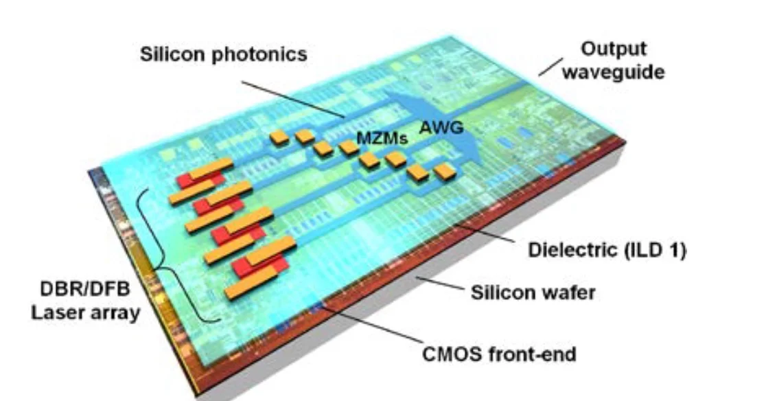
The silicon photonics manufacturing process involves using a silicon-on-insulator (SOI) wafer to implement the passive photonics functions and the electronics. The electronics supports high-speed analogue driver transistors and a 0.25-micron BiCMOS process used to implement the chip's control logic and control interfaces.
 Bert Offrein
The laser is constructed by first bonding a thin layer of indium phosphide. “It is structured in such a way that it [the III-V material] can be embedded completely in the whole CMOS processing,” says Offrein.
The indium phosphide layer, referred to as a III-V membrane, sits on a thin dielectric layer placed on the SOI wafer. The dielectric material is needed to protect the wafer from contamination by the III-V material and ensure that such a design could be manufactured in a BiCMOS foundry.
Once the thin indium phosphide layer is deposited, the laser can be constructed. The final stages, part of the chip-making back-end process, is the adding of metallisation layers that connect the laser and the electronics, and the circuits to the interface signals.
Growing lasers on silicon
Growing the indium phosphide layer directly on silicon, as will be done for the third demonstrator, is more exploratory. “We want to show there is a path forward on this III-V-on-silicon technology to reduce the cost further,” says Offrein.
 Lars Zimmermann
The challenge growing indium phosphide on silicon is the lattice mismatch that occurs between the two materials which leads to defects.
To tackle the issue, an approach known as confined growth is used. A small ‘seed’ is put on the silicon to act as a growth point for the indium phosphide. A small cavity is created using silica to confine the resulting growth. “The material grows in this glass cavity and the defects grow out and disappear at the edges,” says Offrein. “You then have a very high-quality III-V in this glass and this is the starting point to continue to build the quantum wells that we need.”
One challenge is enlarging the confined growth area. So far, such growth is limited to a micron whereas the length of a laser can be 500 microns typically. And once the laser is built, there remain the issues of laser reliability and temperature stability. “We will see challenges but we are not there yet,” says Offrein.
This is the true embodiment of what people first pictured as silicon photonics: the combination of optics and electronics on a single chip
Status
Dimension is tackling designs for communications but such on-chip lasers will also be useful for a range of applications such as optical sensing, says Offrein.
The project is coming to the end of its first year. Its members are creating the basic building blocks needed to realise the lasers on the silicon wafer. IBM has demonstrated the basic functionality by bonding indium phosphide to its own passive silicon photonics technology. “We have also realised the first lasers - not yet electrically pumped but optically pumped,” says Offrein. The performance of these lasers is now being characterised.
All the processes needed to pump the lasers electrically are now in place and the goal is to build complete laser structures by March 2017.
IBM is also working with IHP to see what is required to implement the technology using IHP’s own silicon photonics process. IHP is currently testing IBM’s wafers regarding any contamination issues before testing the integration process.
ADVA Optical Networking would not be on board if they were not expecting eventually to have such technology available for their products
Exploitation
The European Commission has a long history of programmes backing leading-edge research. However, Europe's track record of exploiting such research to achieve market-leading companies and products has been limited.
The European Commission staff involved in planning the Horizon 2020 projects have been far more active in ensuring that these projects are exploited, says Zimmermann. "ADVA Optical Networking would not be on board if they were not expecting eventually to have such technology available for their products," he adds.
If Dimension proves successful, IHP could make available the integrated silicon photonics process to companies to implement their opto-electronic integrated circuit designs.
IBM, while no longer a semiconductor manufacturer, would also be keen for the technology to be transferred to large foundries such as STMicroelectronics and GlobalFoundries. “That way we could purchase the technology and apply it in our own systems,” says Offrein.
Article amended on Nov 29th. Added details about the proof-of-concept demonstrators.
Former Compass Networks staff look to silicon photonics
The Compass Networks team that designed a novel chip with optical input-output is exploring new opportunities now that the IP core router venture has closed it doors.
The team plans to develop chips using silicon photonics for input-output and is involved in a European Commission (EC) Horizon 2020 project dubbed L3Matrix that will make such a chip for the data centre.
 Kobi HasharoniCompass Network was the first company to sell a commercial product - an IP core router - that used an ASIC co-packaged with optics. The IP router was sold to several leading service providers including NTT Communications and Comcast but the venture ultimately failed.
Compass Networks has now become a software company, while its chip R&D team decided to spin off to keep the co-packaged IC and photonics technology alive.
Compass Networks
The ambitious Israeli start-up, Compass Networks, developed its IP core router to compete with the likes of Cisco Systems, Juniper Networks, Alcatel-Lucent (now Nokia) and Chinese giant, Huawei.
Using the chip - a traffic manager with optical input-output - resulted in a smaller, lower-power IP core router design. However, despite the compact platform enabled by the chip, the company failed commercially. The main issue was not the router hardware but the size of Compass Networks’ software team: its 60 engineers could not compete with its much larger IP core router rivals, says Kobi Hasharoni, who was director of electro-optics at Compass Networks.
An IP router takes traffic in the form of packets on its input ports and forwards them to their destination via its output ports. To do this, two functions are used: a network processor unit and a traffic manager. The two functions can be integrated in a single chip or, typically for core routers, implemented using two devices.
The network processor chip performs the packet processing, taking each packet’s header and using a look-up routing table to update the header with the destination address before sending the packet on its way.
The second chip, the traffic manager, oversees billions of packets. The chip implements the queueing protocols and, based on a set of rules, determines which packets have priority on what ports. In a conventional IP router there is also a switch fabric which connects the router cards to be able to send the packets to the required output port.
Compass Networks designed the router between 2007 and 2010. The design team chose the EZchip 100-gigabit NP-4 network processor for the router but developed its own complex traffic manager ASIC, adding the twist of optics for the chip’s input-output.
We didn’t have a backplane; our backplane was just fibres
The resulting chip - referred to as icPhotonics or the D-chip - performed the roles of both traffic manager and switch fabric.
Instead of the traffic manager going through switch fabrics chips and an electrical backplane to a traffic manager on another card, each traffic manager had sufficient bandwidth due to the optics to connect to all the other traffic managers in a mesh configuration.
“We didn’t have a backplane,” says Hasharoni. “Our backplane was just fibres.” Avoiding a backplane resulted in a more compact, lower-power IP core router that saved on operational costs.
D-chip
To make the D-chip, Compass developed a mixed signal ASIC. The 21x21 mm chip comprised the traffic manager and a matrix of analogue circuitry to interface to the optics.
The company used 168 vertical-cavity surface-emitting lasers (VCSELs) and 168 photo-detectors in a 2D array that was positioned above the analogue circuitry; each optical device positioned above its own analogue driver or receiver circuitry. Two ribbon cables, one for the VCSELs and one for the photo-detectors, were then connected to the chip.
VCSELs were at 10 gigabit-per-second (Gbps) at the time and Compass Networks chose to operate them at 8Gbps. “Going to 8 gigabit-per-second seemed reasonable,” says Hasharoni.
Each NP-4 processed 100Gbps of traffic and sent out 160Gbps to the D-chip. The extra traffic included forward error correction and overhead bits to speed up queueing.
The core router platform comprised four line cards, each card having two 100-gigabit NP-4s and two D-chips.
The total optical input-output bandwidth of each D-chip was 1.34 terabits in each direction. The 168 VCSELs were used in such a way that each group of 20 VCSELs supported the 160-gigabit stream of packets, enabling each D-chip to connect directly to the seven other D-chips in a fully connected mesh, while the 28 remaining VCSELs were used for redundancy.
At some point you will not get all this input-output into the ASIC
Silicon photonics
Were the team to tackle a similar design today, the designers would use silicon photonics instead of VCSELs, says Hasharoni. A silicon photonics design would support single-mode fibre and its associated longer reach, while the co-packaging would be easier given both the ASIC and the optics are silicon-based.
Hasharoni points to the rapid development in the capacity of switch chips used in the data centre. Current Ethernet switch silicon from the likes of Broadcom support 3.2 terabits of capacity and this will double in 2017 and double again to 12.8 terabits in 2018. There is even talk of 25.6 terabits switching silicon by 2020.
The issue, however, is that the input-output required for these higher-capacity chips consume more and more power; at 12.8 terabits it will be over half of chip's overall power consumption. "At some point you will not get all this input-output into the ASIC," says Hasharoni.
Using a co-packaged electronics and silicon photonics design, the input-output's power consumption will be halved, says Hasharoni. The optical density is also an order of magnitude higher, thus only a fraction of the ASIC area is used for chip input-output compared to conventional electrical input-ouput. And the resulting switch will not need optical transceivers. "The fibre goes out directly from the IC; the power saving is huge," says Hasharoni.
The EC Horizon 2020 L3Matrix project also includes IBM Research, the Fraunhofer Institute for Reliability and Microintergration (Fraunhofer IZM) and several universities. The project will use embedded III-V light sources on a silicon substrate along with optical modulators. The aim of the design is to develop low-latency, high-radix switch elements using 25Gbps single-mode fibres and waveguides.
"The novel thing here is the use of two-dimensional silicon photonics matrices on an ASIC," says Hasharoni.