
OpenLight's integrated-laser silicon photonics platform

- OpenLight is an independent silicon photonics company backed by Synopsys and Juniper Networks
- The company was created by carving out the silicon photonics arm of Juniper
- The establishment of OpenLight and its open platform highlights the growing maturity of silicon photonics as new applications emerge beyond datacom and telecom
OpenLight is coming to market with an open silicon photonics platform that includes integrated lasers and gain blocks.
Juniper has a long relationship with Synopsys, using its electronic-photonic design automation (EPDA) tools.
So when Juniper said it was spinning out its silicon photonics group, Synopsys was keen to partner. The result is OpenLight, of which Synopsys has a 75 per cent stake costing $67.5 million.
Thomas Mader, OpenLight’s chief operating officer and formerly head of Juniper’s silicon photonics unit, says OpenLight is the first company to offer an open platform that includes monolithically integrated lasers, optical amplifiers and modulators.
Juniper Networks and Synopsys
Juniper gained its silicon photonics technology in 2016 when it acquired Aurrion for $165 million.
Aurrion was a fabless silicon photonics start-up from the University of California, Santa Barbara, with a heterogeneous integration silicon photonics process that includes III-V materials, enabling integrated lasers as part of a photonic circuit.
OpenLight is now making this technology available through its partnership with the foundry Tower Semiconductor.
Juniper’s interests are mainly datacom and telecom, but it recognises the emerging opportunities for silicon photonics such as Lidar, optical computing, high-performance computing and optical interconnect.
“With this kind of technology, you want to drive volumes,” says Mader.

Juniper saw spinning out the unit and opening up access to the technology as the best way to drive volumes and reduce costs. The arrangement also benefits Juniper’s own technology needs.
Synopsys, meanwhile, believes it is the right time to back the OpenLight venture.
“We think it [the open platform] is a great opportunity for growth for Synopsys’s EPDA tools,” says John Koeter, senior vice president of marketing and strategy, solutions group at Synopsys.
OpenLight will give Synopsys insight into how the market is evolving and benefit the company’s tools and, eventually, its IP.
Business model
OpenLight is licensing its process design kit (PDK), the files that model Tower’s fabrication process. A company can enter into an agreement with Tower, access the PDK and design its silicon photonics device.
“What we are offering through Tower, and what we spent significant effort developing and showing Tower how to do, is monolithically integrating lasers and optical gain,” says Mader. “Tower is the first time we’re on a volume eight-inch [wafer] process.”
Juniper entered into a partnership with Tower Semiconductor in 2019.
“We are doing the first MPW [multi-project wafer] this summer with Tower on this process,” says Mader.
OpenLight is also providing designs it has developed and validated for several customers. “But we are not selling PICs [photonic integrated circuits]; that is not part of our plan,” says Mader.
OpenLight intends to partner with other foundries to make more widely available integrated-laser designs.

For now, though, OpenLight is focussed on ratifying its roadmap for the next two years.
“We’re going to be busy building out the component library for Tower to keep customers interested because better components make better circuits,” says Daniel Sparacin, vice president of business development and strategy at OpenLight.
OpenLight offers a 100-gigabit modulator and is working on its next-generation 200-gigabit modulator.
“We’re mostly O-band right now, and we have C-band coming up in the roadmap very shortly,” says Sparacin.
Applications
OpenLight has 400 and 800-gigabit optical designs for the data centre to help customers bring to market their PIC developments.
The company is also seeing interest from Lidar customers, particularly those pursuing coherent-based designs.
“The main reason is the integrated laser,” says Mader. “Otherwise, with standard silicon photonics, you have to attach a laser separately, which doesn’t scale well to multiple channels.” That’s because attaching multiple lasers impacts yield.
Lidar also benefits from on-chip optical amplification. “When you have a complex chip, you have a lot of losses,” says Mader.
OpenLight is working with firms pursuing optical computing for machine learning which promises greater power efficiency. “There are several of them coming to us because we can put hundreds or thousands of indium phosphide elements monolithically on a chip,” says Mader.
OpenLight says it has no position regarding co-packaged optics and whether a design uses an external light source or integrated lasers.
It believes co-packaged optics designs will eventually use integrated light sources, but its technology supports both and can even be used to make external light sources.
Overall, OpenLight says it is working with dozens of companies.
Design tools and integration
Synopsys has been an early mover with its integrated optical design automation tools. The tools include:
- OptoCompiler, a photonic IC design environment.
- The OptSim photonic circuit and system simulator.
- The Sentaurus TCAD and RSoft Photonic Device tools for process modelling and device design.
Working closely with OpenLight will benefit Synopsys’s tool environment, says Koeter. Synopsys is adding functionalities and design capabilities to its tools to support the integration of lasers. OpenLight is also providing Synopsys feedback on what will improve the experience of using its design platform.
Synopsys is one of three leading electronic design automation (EDA) tool companies. However, design tools for photonics are a more recent development.
“EDA quite a while ago is where photonic design is now going,” says Mader.
Integration is the underlying trend driving optics.
“We see the scaling already with 400- and 800-gigabit for datacom and some of the other applications; you see the shift to silicon photonics,” says Mader. “The higher the complexity, the more you see it shifting this way because there’s a cost advantage with the integrated laser and optical gain.”
Photonics may not come close to chip designs with billions of transistors. Still, photonic designs that go beyond four-channel design to ones with 32 or 64 channels or optical computing with hundreds or thousands of components are emerging.
“So you see a scaling even though it’s decades behind the electronics field,” says Mader.
With monolithically integrated lasers, yields remain high, whereas scaling a design with discrete components results in unacceptable yields.
“And so we will be able to go where you can’t go otherwise,” says Mader. “It’s not billions, but even dozens [of components] at this point is revolutionary.”

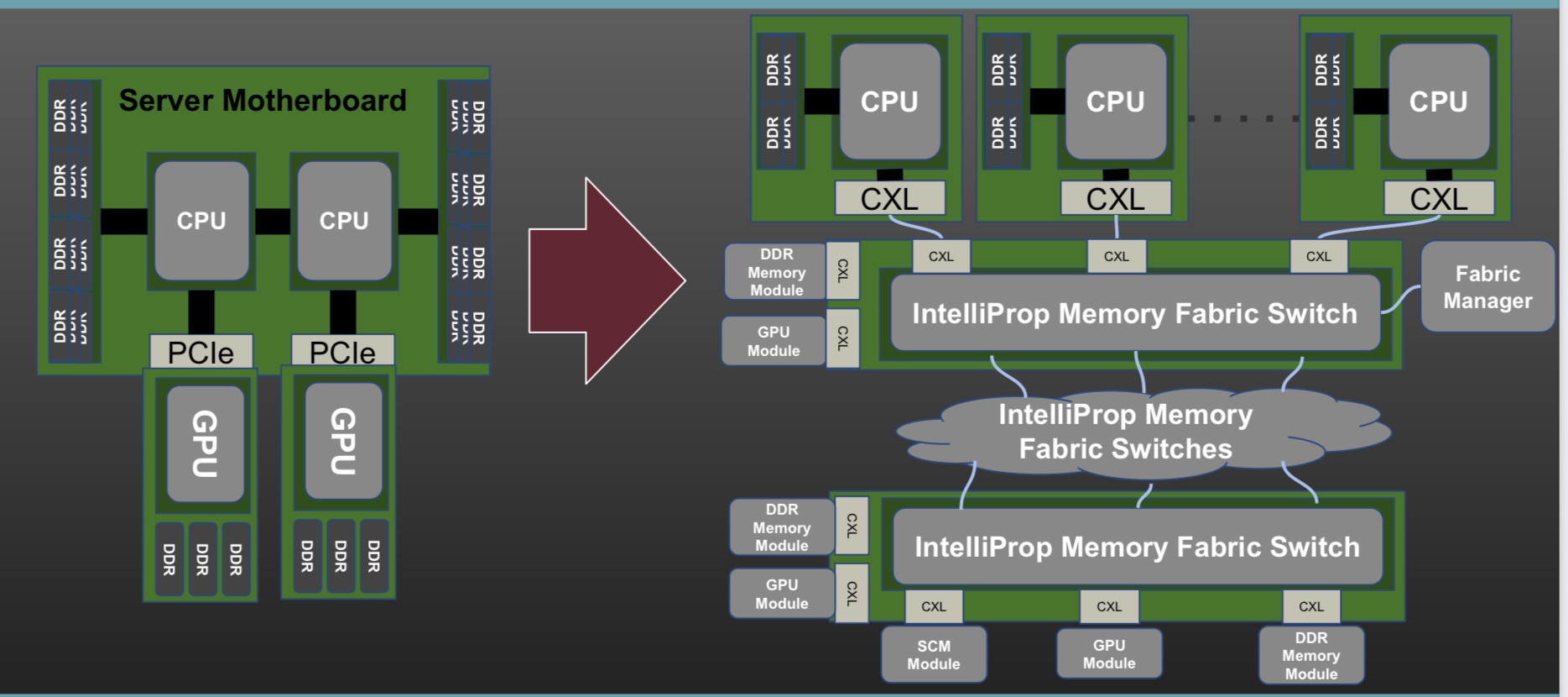
Data centre disaggregation with Gen-Z and CXL

Part 1: CXL and Gen-Z
- The Gen-Z and Compute Express Link (CXL) protocols have been shown working in unison to implement a disaggregated processor and memory system at the recent Supercomputing 21 show.
- The Gen-Z Consortium’s assets are being subsumed within the CXL Consortium. CXL will become the sole industry standard moving forward.
- Microsoft and Meta are two data centre operators backing CXL.
Pity Hiren Patel, tasked with explaining the Gen-Z and CXL networking demonstration operating across several booths at the Supercomputing 21 (SC21) show held in St. Louis, Missouri in November.
Not only was Patel wearing a sanitary mask while describing the demo but he had to battle to be heard above cooling fans so loud, you could still be at St. Louis Lambert International Airport.
Gen-Z and CXL are key protocols supporting memory and server disaggregation in the data centre.
The SC21 demo showed Gen-Z and CXL linking compute nodes to remote ‘media boxes’ filled with memory in a distributed multi-node network (see diagram, bottom).
CXL was used as the host interface on the various nodes while Gen-Z created and oversaw the mesh network linking equipment up to tens of meters apart.
“What our demo showed is that it is finally coming to fruition, albeit with FPGAs,” says Patel, CEO of IP specialist, IntelliProp, and President of the Gen-Z Consortium.
Interconnects
Gen-Z and CXL are two of a class of interconnect schemes announced in recent years.
The interconnects came about to enable efficient ways to connect CPUs, accelerators and memory. They also address a desire among data centre operators to disaggregate servers so that key components such as memory can be pooled separately from the CPUs.
The idea of disaggregation is not new. The Gen-Z protocol emerged from HPE’s development of The Machine, a novel memory-centric computer architecture. The Gen-Z Consortium was formed in 2016, backed by HPE and Dell, another leading high-performance computing specialist. The CXL consortium was formed in 2019.
Other interconnects of recent years include the Open Coherent Accelerator Processor Interface (Open-CAPI), Intel’s own interconnect scheme Omni-Path which it subsequently sold off, Nvidia’s NVLink, and the Cache Coherent Interconnect for Accelerators (CCIX).
The emergence of the host buses was also a result of industry frustration with the prolonged delay in the release of the then PCI Express (PCIe) 4.0 specification.
All these interconnects are valuable, says Patel, but many are implemented in a proprietary manner whereas CXL and Gen-Z are open standards that have gained industry support.
“There is value moving away from proprietary to an industry standard,” says Patel.
Merits of pooling
Disaggregated designs with pooled memory deliver several advantages: memory can be upgraded at different stages to the CPUs, with extra memory added as required. “Memory growth is outstripping CPU core growth,” says Patel. “Now you need banks of memory outside of the server box.”
A disaggregated memory architecture also supports multiple compute nodes – CPUs and accelerators such as graphics processor units (GPUs) or FPGAs – collaborating on a common data set.
Such resources also become configurable: in artificial intelligence, training workloads require a hardware configuration different to inferencing. With disaggregation, resources can be requested for a workload and then released once a task is completed.
Memory disaggregation also helps data centre operators drive down the cost-per-bit of memory. “What data centres spend just on DRAM is extraordinarily high,” says Erich Hanke, senior principal engineer, storage and memory products, at IntelliProp.
Memory can be used more efficiently and need no longer to be stranded. A server can be designed for average workloads, not worse case ones as is done now. And when worst-case scenarios arise, extra memory can be requested.

“This allows the design of efficient data centres that are cost optimised while not losing out on the aggregate performance,” says Hanke.
Hanke also highlights another advantage, minimising data loss during downtimes. Given the huge number of servers in a data centre, reboots and kernel upgrades are a continual occurrence. With disaggregated memory, active memory resources need not be lost.
Gen-Z and CXL
The Gen-Z protocol allows for the allocation and deallocation of resources, whether memory, accelerators or networking. “It can be used to create a temporary or permanent binding of that resource to one or more CPU nodes,” says Hanke.
Gen-Z supports native peer-to-peer requests flowing in any direction through a fabric, says Hanke. This is different to PCIe which supports tree-type topologies.
Gen-Z and CXL are also memory-semantic protocols whereas PCIe is not.
With a memory-semantic protocol, a processor natively issues data loads and stores into fabric-attached components. “No layer of software or a driver is needed to DMA (direct memory access) data out of a storage device if you have a memory-semantic fabric,” says Hanke.
Gen-Z is also hugely scalable. It supports 4,096 nodes per subnet and 64,000 subnets, a total of 256 million nodes per fabric.
The Gen-Z specification is designed modularly, comprising a core specification and other components such as for the physical layer to accommodate changes in serialiser-deserialiser (serdes) speeds.
For example, the SC21 demo using an FPGA implemented 25 giga-transfers a second (25GT/s) but the standard will support 50 and 112GT/s rates. In effect, the Gen-Z specification is largely done.
What Gen-Z does not support is cache coherency but that is what CXL is designed to do. Version 2.0 of the CXL specification has already been published and version 3.0 is expected in the first half of 2022.
CXL 2.0 supports three protocols: CXL.io which is similar to PCIe – CXL uses the physical layer of the PCIe bus, CXL.memory for host-memory accesses, and CXL.cache for coherent host-cache accesses.
“More and more processors will have CXL as their connect point,” says Patel. “You may not see Open-CAPI as a connect point, you may not see NVLink as a connect point, you won’t see Gen-Z as a connect point but you will see CXL on processors.”
SC21 demo
The demo’s goal was to show how computing nodes – hosts – could be connected to memory modules through a switched Gen-Z fabric.
The equipment included a server hosting the latest Intel Sapphire Rapids processor, a quad-core A53 ARM processor on a Xilinx FPGA implemented with a Bittware 250SoC FPGA card, as well as several media boxes housing memory modules.
The ARM processor was used as the Fabric Manager node which oversees the network to allow access to the storage endpoints. There is also a Fabric Adaptor that connects to the Intel processor’s CXL bus on one side and the other to the memory-semantic fabric.
“CXL is in the hosts and everything outside that is Gen-Z,” says Patel.
The CXL V1.1 interface is used with four hosts (see diagram below). The V1.1 specification is point-to-point and as such can’t be used for any of the fabric implementations, says Patel. The 128Gbps CXL host interfaces were implemented as eight lanes of 16Gbps, using the PCIe 4.0 physical layer.
The Intel Sapphire Rapids processor supports a CXL Gen5x16 bus supporting 512Gbps (PCIe 5.0 x 16 lanes) but that is too fast for IntelliProp’s FPGA implementation. “An ASIC implementation of the IntelliProp CXL host fabric adapter would run at the 512Gpbs full rate,” says Patel. With an ASIC, the Gen-Z port court could be increased from 12 to 48 ports while the latency of each hop would be 35ns only.
The media box is a two-rack-unit (2RU) server without a CPU but with fabric-attached memory modules. Each memory module has a switch that enables multipath accesses. A memory module of 256Gbytes could be partitioned across all four hosts, for example. Equally, memory can be shared among the hosts. In the SC21 demo, memory in a media box was accessed by a server 30m away.
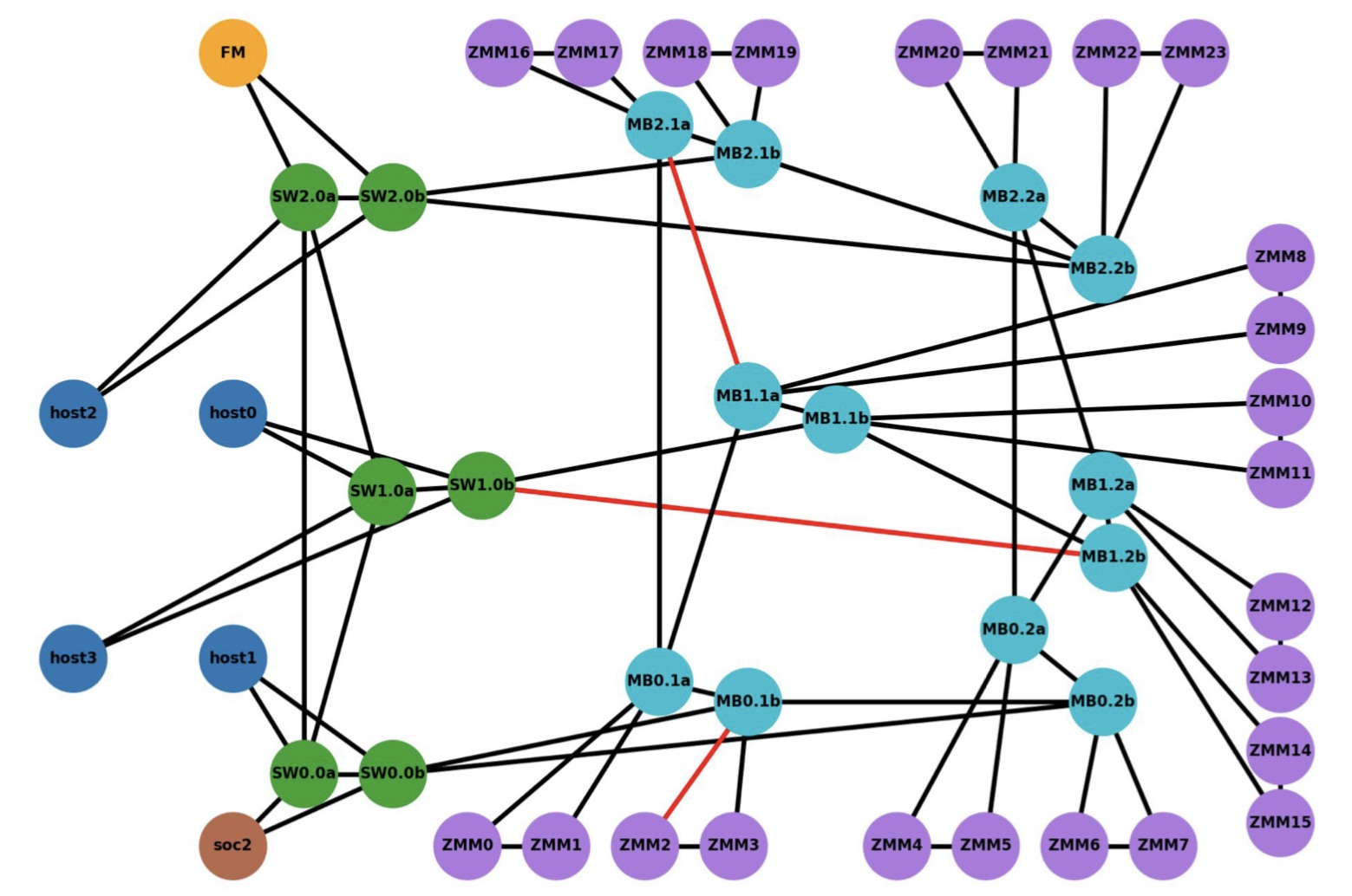
IntelliProp implemented the Host Fabric Adapter which included integrated switching, a 12-port Gen-Z switch, and the memory modules featuring integrated switching. All of the SC21 demonstration, outside of the Intel host, was done using FPGAs.
For a data centre, the media boxes would connect to a top-of-rack switch and fan out to multiple servers. “The media box could be co-located in a rack with CPU servers, or adjacent racks or a pod,” says Hanke.
The distances of a Gen-Z network in a data centre would typically be a row- or pod-scale, says Hanke. IntelliProp has had enquiries about going greater distances but above 30m fibre length starts to dictate latency. It’s a 10ns round trip for each meter of cable, says IntelliProp.
What the demo also showed was how well the Gen-Z and CXL protocols combine. “Gen-Z converts the host physical address to a fabric address in a very low latency manner; this is how they will eventually blend,” says Hanke.
What next?
The CXL Consortium and The Gen-Z Consortium signed a memorandum of understanding in 2020 and now Gen-Z’s assets are being transferred to the CXL Consortium. Going forward, CXL will become the sole industry standard.
Meanwhile, Microsoft, speaking at SC21, expressed its interest in CXL to support disaggregated memory and to grow memory dynamically in real-time. Meta is also backing the standard. But both cloud companies need the standard to be easily manageable (software) and stress the importance that CXL and its evolutions have minimal impact on overall latency.

Turning to optical I/O to open up computing pinch points

Getting data in and out of chips used for modern computing has become a key challenge for designers.
A chip may talk to a neighbouring device in the same platform or to a chip across the data centre.
The sheer quantity of data and the reaches involved – tens or hundreds of meters – is why the industry is turning to optical for a chip’s input-output (I/O).
It is this technology transition that excites Ayar Labs.
The US start-up showcased its latest TeraPHY optical I/O chiplet operating at 1 terabit-per-second (Tbps) during the OFC virtual conference and exhibition held in June.
Evolutionary and revolutionary change
Ayar Labs says two developments are driving optical I/O.
One is the exponential growth in the capacity of Ethernet switch chips used in the data centre. The emergence of 25.6-terabit and soon 51.2-terabit Ethernet switches continue to drive technologies and standards.
This, says Hugo Saleh, vice president of business development and marketing, and recently appointed as the managing director of Ayar Labs’ new UK subsidiary, is an example of evolutionary change.
But artificial intelligence (AI) and high-performance computing have networking needs independent of the Ethernet specification.
“Ethernet is here to stay,” says Saleh. “But we think there is a new class of communications that is required to drive these advanced applications that need low latency and low power.”
Manufacturing processes
Ayar Labs’ TeraPHY chiplet is manufactured using GlobalFoundries’ 45nm RF Silicon on Insulator (45RFSOI) process. But Ayar Labs is also developing TeraPHY silicon using GlobalFoundries’ emerging 45nm CMOS-silicon photonics CLO process (45CLO).
The 45RFSOI process is being used because Ayar Labs is already supplying TeraPHY devices to customers. “They have been going out quite some time,” says Saleh.
But the start-up’s volume production of its chiplets will use GlobalFoundries’ 45CLO silicon photonics process. Version 1.0 of the process design kit (PDK) is expected in early 2022, leading to qualified TeraPHY parts based on the process.
One notable difference between the two processes is that 45RFSOI uses a vertical grating coupler to connect the fibre to the chiplet which requires active alignment. The 45CLO process uses a v-groove structure such that passive alignment can be used, simplifying and speeding up the fibre attachment.
“With high-volume manufacturing – millions and even tens of millions of parts – things like time-in-factory make a big difference,” says Saleh. Every second spent adds cost such that the faster the processes, the more cost-effective and scalable the manufacturing becomes.
Terabit TeraPHY
The TeraPHY chiplet demonstrated during OFC uses eight optical transceivers. Each transceiver comprises eight wavelength-division multiplexed (WDM) channels, each supporting 16 gigabit-per-second (Gbps) of data. The result is a total optical I/O bandwidth of 1.024Tbps operating in each direction (duplex link).
“The demonstration is at 16Gbps and we are going to be driving up to 25Gbps and 32Gbps next,” says Saleh.
The chiplet’s electrical I/O is slower and wider: 16 interfaces, each with 80, 2Gbps channels implementing Intel’s Advanced Interface Bus (AIB) technology.
Last December, Ayar Labs showcased advanced parts using the CLO process. The design was a direct-drive part – a prototype of a future-generation product, not the one demonstrated for OFC.
“The direct-drive part has a serial analogue interface that could come from the host ASIC directly into the ring resonators and modulate them whereas the part we have today is the productised version of an AIB interface with all the macros and all the bandwidth enabled,” says Saleh.
Ayar Labs also demonstrated its 8-laser light source, dubbed SuperNova, that drives the chiplet’s optics.
The eight distributed feedback (DFB) lasers are mixed using a planar lightwave circuit to produce eight channels, each comprising eight frequencies of light.
Saleh compares the SuperNova to a centralised power supply in a server that power pools of CPUs and memory. “The SuperNova mimics that,” he says. “One SuperNova or a 1 rack-unit box of 16 SuperNovas distributing continuous-wave light just like distributed voltage [in a server].”
The current 64-channel SuperNova powers a single TeraPHY but future versions will be able to supply light to two or more.
Ayar Labs is using Macom as its volume supplier of DFB lasers.
Significance
Ayar Labs believes the 1-terabit chip-to-chip WDM link is an industry first.
The demo also highlights how the company is getting closer to a design that can be run in the field. The silicon was made less than a month before the demonstration and was assembled quickly. “It was not behind glass and was operating at room temperature,” says Saleh. “It’s not a lab setting but a production setting.”
The same applies to the SuperNova. The light source is compliant with the Continuous-Wave Wavelength Division Multiplexing (CW-WDM) Multi-Source Agreement (MSA) Group that released its first specification revision to coincide with OFC. The CW-WDM MSA Group has developed a specification for 8, 16, and 32-wavelength optical sources.
The CW-WDM MSA promoter and observer members include all the key laser makers as well as the leading ASIC vendors. “We hope to establish an ecosystem on the laser side but also on the optics,” says Saleh.
“Fundamentally, there is a change at the physical (PHY) level that is required to open up these bottlenecks,” says Saleh. “The CW-WDM MSA is key to doing that; without the MSA you will not get that standardisation.”
Saleh also points to the TeraPHY’s optical I/O’s low power consumption which for each link equates to 5pJ/bit. This is about a tenth of the power consumed by electrical I/O especially when retimers are used. Equally, the reach is up to 2km not tens of centimetres associated with electrical links.
Chiplet demand
At OFC, Arista Networks outlined how pluggable optics will be able to address 102.4 terabit Ethernet switches while Microsoft said it expects to deploy co-packaged optics by the second half of 2024.
Nvidia also discussed how it clusters its graphics processing units (GPUs) that are used for AI applications. However, when a GPU from one cluster needs to talk to a GPU in another cluster, a performance hit occurs.
Nvidia is looking for the optical industry to develop interfaces that will enable its GPU systems to scale while appearing as one tightly coupled cluster. This will require low latency links. Instead of microseconds and milliseconds depending on the number of hops, optical I/O reduces the latency to tens of nanoseconds.
“We spec our chiplet as sub-5ns plus the time of flight which is about 5ns per meter,” says Saleh. Accordingly, the transit time between two GPUs 1m apart is 15ns.
Ayar Labs says that after many conversations with switch vendors and cloud players, the consensus is that Ethernet switches will have to adopt co-packaged optics. There will be different introductory points for the technology but the industry direction is clear.
“You are going to see co-packaged optics for Ethernet by 2024 but you should see the first AI fabric system with co-packaged I/O in 2022,” says Saleh.
Intel published a paper at OFC involving its Stratix 10 FPGA using five Ayar Labs’ chiplets, each one operating at 1.6 terabits (each optical channel operating at 25Gbps, not 16Gbps). The resulting FPGA has an optical I/O capacity of 8Tbps, the design part of the US DARPA PIPES (Photonics in the Package for Extreme Scalability) project.
“A key point of the paper is that Intel is yielding functional units,” says Saleh. The paper also highlighted the packaging and assembly achievements and the custom cooling used.
Intel Capital is a strategic investor in Ayar Labs, as is GlobalFoundries, Lockheed Martin Ventures, and Applied Materials.

Ayar Labs’ TeraPhy chiplet nears volume production
Moving data between processing nodes - whether servers in a data centre or specialised computing nodes used for supercomputing and artificial intelligence (AI) - is becoming a performance bottleneck.
Workloads continue to grow yet networking isn’t keeping pace with processing hardware, resulting in the inefficient use of costly hardware.
Networking also accounts for an increasing proportion of the overall power consumed by such computing systems.
These trends explain the increasing interest in placing optics alongside chips and co-packaging the two to boost input-output (I/O) capacity and reach.
At the ECOC 2020 exhibition and conference held virtually, start-up Ayar Labs showcased its first working TeraPHY, an optical I/O chiplet, manufactured using GlobalFoundries’ 45nm silicon-photonics process.
GlobalFoundries is a strategic investor in Ayar Labs and has been supplying Ayar Labs with TeraPHY chips made using its existing 45nm silicon-on-insulator process for radio frequency (RF) designs.
The foundry’s new 300mm wafer 45nm silicon-photonics process follows joint work with Ayar Labs, including the development of the process design kit (PDK) and standard cells.
“This is a process that mixes optics and electronics,” says Hugo Saleh, vice president of marketing and business development at Ayar Labs (pictured). “We build a monolithic die that has all the logic to control the optics, as well as the optics,” he says.
The latest TeraPHY design is an important milestone for Ayar Labs as it looks to become a volume supplier. “None of the semiconductor manufacturers would consider integrating a solution into their package if it wasn’t produced on a qualified high-volume manufacturing process,” says Saleh.
Applications
The TeraPHY chiplet can be co-packaged with such devices as Ethernet switch chips, general-purpose processors (CPUs), graphics processing units (GPUs), AI processors, and field-programmable gate arrays (FPGAs).
Ayar Labs says it is engaged in several efforts to add optics to Ethernet switch chips, the application most associated with co-packaged optics, but its focus is AI, high-performance computing and aerospace applications.
Last year, Intel and Ayar Labs detailed a Stratix 10 FPGA co-packaged with two TeraPHYs for a phased-array radar design as part of a DARPA PIPES and the Electronics Resurgence Initiative backed by the US government.
Adding optical I/O chiplets to FPGAs suits several aerospace applications including avionics, satellite and electronic warfare.
TeraPHY chiplet
The ECOC-showcased TeraPHY uses eight transmitter-receiver pairs, each pair supporting eight channels operating at either 16, 25 or 32 gigabit-per-second (Gbps), to achieve an optical I/O of up to 2.048 terabits.
The chiplet can use either a serial electrical interface or Intel’s Advanced Interface Bus (AIB), a wide-bus design that uses slower 2Gbps channels. The latest TeraPHY uses a 32Gbps non-return-to-zero (NRZ) serial interface and Saleh says the company is working on a 56Gbps version.
The company has also demonstrated 4-level pulse-amplitude modulation (PAM-4) technology but many applications require the lowest latency links possible.
“PAM-4 gives you a higher data rate but it comes with the tax of forward-error correction,” says Saleh. With PAM-4 and forward-error correction, the latency is hundreds of nanoseconds (ns), whereas the latency is 5ns using a NRZ link.
Ayar Labs’s next parallel I/O AIB-based TeraPHY design will use Intel’s AIB 1.0 specification and will use 16 cells, each having 80, 2Gbps channels, to achieve a 2.5Tbps electrical interface.
In contrast, the TeraPHY used with the Stratix 10 FPGA has 24 AIB cells, each having 20, 2Gbps channels for an overall electrical bandwidth of 960 gigabits, while its optical I/O is 2.56Tbps since 10 transmit-receive pairs are used.
The optical bandwidth is deliberately higher than the electrical bandwidth. First, not all the transmit-receive macros on the die need to be used. Second, the chiplet has a crossbar switch that allows one-to-many connections such that an electrical channel can be sent out on more than one optical interface and vice versa.
Architectures
Saleh points to several recent announcements that highlight the changes taking place in the industry that are driving new architectural developments.
He cites AMD acquiring programmable logic player, Xilinx; how Apple instances are now being hosted in Amazon Web Services’ (AWS) cloud to aid developers and Apple's processors, and how AWS and Microsoft are developing their own processors.
“Processors can now be built by companies using TSMC’s leading process technology using the ARM and RISC-V processor ecosystems,” he says. “AWS and Microsoft can target their codebase to whatever processor they want, including one developed by themselves.”
Saleh notes that Ethernet remains a key networking technology in the data centre and will continue to evolve but certain developments do need something else.
Applications such as AI and high-performance computing would benefit from a disaggregated design whereby CPUs, GPUs, AI devices and memory are separated and pooled. An application can then select the hardware it needs for the relevant pools to create the exact architecture it needs.
“Some of these new applications and processors that are popping up, there is a lot of benefit in a one-to-one and one-to-many connections,” he says. “The Achilles heel has always been how you disaggregate the memory because of latency and power concerns. Co-packaged optics with the host ASIC is the only way to do that.”
It will also be the only way such disaggregated designs will work given that far greater connectivity - estimated to be up to 100x that of existing systems - will be needed.
Expansion
Ayar Labs announced in November that it had raised $35 million in the second round of funding which, it says, was oversubscribed. This adds to its previous funding of $25 million.
The latest round includes four new investors and will help the start-up expand and address new markets.
One investor is a UK firm, Downing, that will connect Ayar Labs to European R&D and product opportunities. Saleh mentions the European Processor Initiative (EPI) that is designing a family of low-power European processors for extreme-scale computing. “Working with Downing, we are getting introduced into some of these initiatives including EPI and having conversations with the principals,” he says.
In turn, SGInnovate, a venture capitalist funded by the Singapore government, will help expand Ayar Labs’ activities in Asia. The two other investors are Castor Ventures and Applied Ventures, the investment arm of Applied Materials, the supplier of chip fabrication plant equipment.
“Applied Materials want to partner with us to develop the methodologies and tools to bring the technology to market,” says Saleh.
Meanwhile, Ayar Labs continues to grow, with a staff count approaching 100.

Imec eyes silicon photonics to solve chip I/O bottleneck
In the second and final article, the issue of adding optical input-output (I/O) to ICs is discussed with a focus on the work of the Imec nanoelectronics R&D centre that is using silicon photonics for optical I/O.
Part 2: Optical I/O
Imec has demonstrated a compact low-power silicon-photonics transceiver operating at 40 gigabits per second (Gbps). The silicon photonics transceiver design also uses 14nm FinFET CMOS technology to implement the accompanying driver and receiver electronics.
 Joris Van Campenhout“We wanted to develop an optical I/O technology that can interface to advanced CMOS technology,” says Joris Van Campenhout, director of the optical I/O R&D programme at Imec. “We want to directly stick our photonics device to that mainstream CMOS technology being used for advanced computing applications.”
Traditionally, the Belgium nanoelectronics R&D centre has focussed on scaling logic and memory but in 2010 it started an optical I/O research programme. “It was driven by the fact that we saw that electrical I/O doesn’t scale that well,” says Van Campenhout. Electrical interfaces have power, space and reach issues that get worse with each hike in transmission speed.
Imec is working with partner companies to research optical I/O. The players are not named but include semiconductor foundries, tool vendors, fabless chip companies and electronic design automation tools firms. The aim is to increase link capacity, bandwidth density - a measure of the link capacity that can be crammed in a given space - and reach using optical I/O. The research’s target is to achieve between a 10x to 100x in scaling.
The number of silicon photonics optical I/O circuits manufactured each year remains small, says Imec, several thousand to ten thousand semiconductor wafers at most. But Imec expects volumes to grow dramatically over the next five years as optical interconnects are used for ever shorter reaches, a few meters and eventually below one meter.
“That is why we are participating in this research, to put together building blocks to help in the technology pathfinding,” says Van Campenhout.
We wanted to develop an optical I/O technology that can interface to advanced CMOS technology
Silicon photonics transceiver
Imec has demonstrated a 1330nm optical transceiver operating at 40Gbps using non-return-to-zero signalling. The design uses hybrid integration to combine silicon photonics with 14nm FinFET CMOS electronics. The resulting transceiver occupies 0.025 mm2, the area across the combined silicon photonics and CMOS stack for a single transceiver channel. This equates to a bandwidth density of 1.6 terabit-per-second/mm2.
The silicon photonics and FinFET test chips each contain circuitry for eight transmit and eight receive channels. Combined, the transmitter path comprises a silicon photonics ring modulator and a FinFET differential driver while the receiver uses a germanium-based photo-detector and a first-stage FinFET trans-impedance amplifier (TIA).
The transceiver has an on-chip power consumption of 230 femtojoules-per-bit, although Van Campenhout stresses that this is a subset of the functionality needed for the complete link. “This number doesn’t include the off-chip laser power,” he says. “We still need to couple 13dBm - 20mW - of optical power in the silicon photonics chip to close the link budget.” Given the laser has an efficiency of 10 to 20 percent, that means another 100mW to 200mW of power.
That said, an equivalent speed electrical interface has an on-chip power consumption of some 2 picojoules-per-bit so the optical interface still has some margin to better the power efficiency of the equivalent electrical I/O. In turn, the optical I/O’s reach using single-mode fibre is several hundred meters, far greater than any electrical interface.
Imec is confident it can increase the optical interface’s speed to 56Gbps. The layout of the CMOS circuits can be improved to reduce internal parasitic capacitances while Imec has already improved the ring modulator design compared to the one used for the demonstrator.
“We believe that with a few design tweaks we can get to 56Gbps comfortably,” says Van Campenhout. “After that, to go faster will require new technology like PAM-4 rather than non-return-to-zero signalling.”
Imec has also tested four transmit channels using cascaded ring modulators on a common waveguide as part of work to add a wavelength-division multiplexing capability.
Transceiver packaging
The two devices - the silicon photonics die and the associated electronics - are combined using chip-stacking technology.
Both devices use micro-bumps with a 50-micron pitch with the FinFET die flip-chipped onto the silicon photonics die. The combined CMOS and silicon photonics assembly is glued on a test board and wire-bonded, while the v-groove fibre arrays are attached using active alignment. The fibre-to-chip coupling loss, at 4.5dB in the demonstration, remains high but the researchers say this can be reduced, having achieved 2dB coupling losses in separate test chips.
 Source: Imec.
Imec is also investigating using through-silicon vias (TSV) technology and a silicon photonics interposer in order to replace the wire-bonding. TSVs deliver better power and ground signals to the two dies and enable high-speed electrical I/O between the transceiver and the ASIC such as a switch chip. The optics and ASIC could be co-packaged or the transceiver used in an on-board optics design next to the chip.
“We have already shown the co-integration of TSVs with our own silicon photonics platform but we are not yet showing the integration with the CMOS die,” says Van Campenhout. “Something we are working on.”
Co-packaging the optics with silicon will come at a premium cost
Applications
The first ICs to adopt optical I/O will be used in the data centre and for high-performance computing. The latest data centre switch ICs, with a capacity of 12.8 terabits, are implemented using 16nm CMOS. Moving to a 7nm CMOS process node will enable capacities of 51.2 terabits. “These are the systems where the bandwidth density challenge is the largest,” says Van Campenhout.
But significant challenges must be overcome before this happens, he says: “I think we all agree that bringing optics deeply integrated into such a product is not a trivial thing.”
Co-packaging the optics with silicon will come at a premium cost. There are also reliability issues to be resolved and greater standardisation across the industry will be needed as to how the packaging should be done.
Van Campenhout expects this will only happen in the next four to five years, once the traffic-handling capacity of switch chips doubles and doubles again.
Imec has seen growing industry interest in optical I/O in the last two years. “We have a lot of active interactions so interest is accelerating now,” says Van Campenhout.
Ayar Labs advances I/O and pens GlobalFoundries deal
Silicon photonics start-up, Ayar Labs, has entered into a strategic agreement with semiconductor foundry, GlobalFoundries.
 Alexandra Wright-GladsteinAyar Labs will provide GlobalFoundries with its optical input-output (I/O) technology. In return, the start-up will gain early access to the foundry’s 45nm CMOS process being tailored for silicon photonics.
GlobalFoundries has also made an investment in the start-up for an undisclosed fee.
“We gain, first and foremost, a close relationship with GlobalFoundries as we qualify our product for customers,” says Alexandra Wright-Gladstein, co-founder and CEO of Ayar Labs. “That will help us speed up availability of our product and have their weight of support behind us.”
Strategy
Ayar Labs is bringing to market technology developed by academics originally at MIT. The research group developed a way to manufacture silicon photonics components using a standard silicon-on-insulator (SOI) CMOS process. The research work resulted in a novel dual-core RISC-V microprocessor demonstrator that used optical I/O to send and receive data, work that was published in the Nature science journal in December 2015.
Ayar Labs is using its optical I/O technology to address the high-performance computing and data centre markets. The optical I/O reaches up to 2km, from chip-to-chip communications to linking equipment between the buildings of a large data centre.
The start-up will offer a die - chiplet - that can be integrated within a multi-chip module, as well as a high-capacity 3.2-terabit optical module.
“We are aggregating the capacity of 4, 8 or 16 pluggable transceivers into a single module to share the cost of production at such high data rates,” says Wright-Gladstein. “This makes us competitive [for applications] where a pluggable transceiver is not.” Offering a chiplet and a high-density optical module on a board will bring to the marketplace the benefits companies are looking for if they are to move from copper to optics, she says.
Ayar Labs will also license its technology. “Our goal is to create an ecosystem for optical I/O for chips,” says Wright-Gladstein.

Technology
Ayar Labs has been a customer of GlobalFoundries for several years, using its existing 45nm SOI CMOS process to make devices as part of the foundry’s multi-project wafer service. The start-up will use the same 45nm CMOS process to make its first product. The CEO points out that using an unmodified electronics process introduces tight design constraints; no new materials can be introduced or layer thicknesses modified.
The start-up will also support GlobalFoundries in the development of its 45nm CMOS process optimised for silicon photonics. “The new process is more geared to traditional applications of optics such as optical transceivers for longer-distance communications,” says Wright-Gladstein.
Our goal is to create an ecosystem for optical I/O for chips
The intellectual property of Ayar Labs includes a micro-ring resonator optical modulator that is tiny compared to a Mach-Zehnder modulator. An issue with a micro-ring resonator is its sensitivity to temperature and manufacturing variances. Ayar’s Labs ability to design the ring resonator using standard CMOS means control circuitry can be added to ensure the modulator’s stability.
Ayar Labs has advanced its technology since the publication of the 2015 Nature paper. It has changed the operating wavelength of its optics from 1180nm to the standard 1310nm. It has also increased the speed of optical transmission from 2.5 to 25 gigabits-per-second (Gbps). The start-up expects to be able to extend the data rate to 50Gbps and even 100Gbps using 4-level pulse-amplitude modulation (PAM-4). The company has already demonstrated PAM-4 technology working with its optics.
The company also has wavelength-division multiplexing technology, using 8 wavelengths on a fibre; the original microprocessor demonstrator used only one wavelength. “We have 8 [micro-resonator] rings that lock on the transmit side and 8 rings that lock on the receive side,” says Wright-Gladstein. The company expects to extend the number of working wavelengths to 16 and even 32.
“We believe this is the process of the future because it can scale,” she says.
A factor of 10
Wright-Gladstein says its technology delivers a tenfold improvement using several metrics when compared to copper interconnect.
Typically a 25Gbps electrical interface will occupy 1 mm2 of chip area whereas Ayar Labs can fit more - potentially much more - than 250Gbps. The use of WDM technology also means that the amount of data passing the chip’s edge is at least 10 times greater.
The energy efficiency for the I/O is also between 5 times and 20 times greater than copper
The latency - how long it takes a signal to arrive at the receiver from the transmitter - is also improved tenfold. The fastest electrical interfaces at 56Gbps that use PAM-4 require forward-error correction which adds 100ns to the latency. Sending light 3m between racks takes 10ns, a tenth of the time. And more wavelengths can be added rather than using PAM-4 to avoid adversely impacting latency. “That matters for HPC customers,” she says.
The energy efficiency for the I/O is also between 5 times and 20 times greater than copper.
Ayar Labs has also developed an integrated laser module that provides the light sources for its optical I/O. Multiple lasers are integrated on a single die and the module outputs several wavelengths of light on several fibres.
The start-up claims the overall optical I/O design is simplified as there is no attachment of laser dies to the silicon and there are no attached driver chips. The result is a die that is flip-chip-attached allowing the use of standard high-volume CMOS packaging techniques.
First samples are expected sometime this year, with general product availability starting in 2019.
Meanwhile, GlobalFoundries is expected to offer the optical I/O as part of its 45nm silicon photonics process library in 2019.
Stitching together disaggregated chips
The Optical Internetworking Forum (OIF) has begun work on a 112-gigabit electrical interface to connect chips in a multi-chip module.
The ultra-short-reach electrical interface for multi-chip modules adds to the OIF's ongoing CEI-112G project, started in August 2016, to develop a 112 gigabit-per-second (Gbps) serial electrical interface for next-generation optical modules.
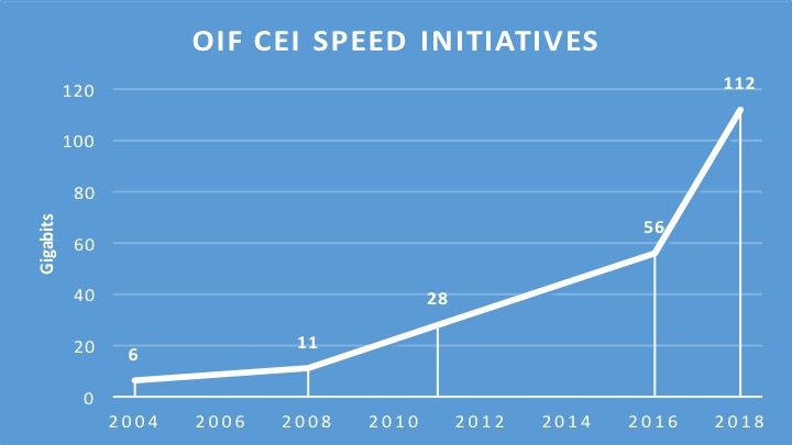 Source: Gazettabyte, OIF data. The year 2018 is an estimate.
The OIF is an industry organisation whose members include telcos, data centre operators, equipment makers and component companies. The OIF undertakes projects that range from high-speed interfaces, optical modules and flexible Ethernet through to programmable interfaces for Transport SDN. Each OIF project culminates in a published Implementation Agreement.
According to David Stauffer, of Kandou Bus and the OIF’s Physical and Link Layer Working Group Chair, the 112G multi-chip module initiative builds on earlier OIF work on a 56-gigabit ultra-short-reach (USR) interface that first addressed die-to-die communication. "We realised that there seems to be more than one application," says Stauffer. "The 112G project is expanded for these applications such that we will possibly end up with different solutions rather than just one."
Multi-chip modules
It was during the 56G USR work that the OIF first heard from members about the challenges of designing a system-on-chip and the idea of taking functions off-chip. High-capacity Ethernet switch chips, for example, are becoming so complex that future designs will not be able to support the long-reach serialisers-deserialisers (SerDes) circuits used for input-output due to the resulting design exceeding the chip's power constraints. “They [chip makers] were starting to think about offloading functions such as SerDes from the system-on-chip,” says Stauffer.
State-of-the-art chip designs can also include functions that occupying significant die area. “To better optimise chip and system costs, people are starting to think about the concept of breaking up the system-on-chip into multiple chips that are better optimised for cost and yield,” says Stauffer. He cites as an example a next-generation system-on-chip that interfaces to long-reach SerDes or optics, performs sensor processing and has significant on-board logic.
 David StaufferThe logic functions of such a chip are best implemented using an advanced 7nm CMOS process, yet SerDes design are not implemented in 7nm and won't be for some time yet. In turn, the sensor array may not even be implemented using a logic process. And if the logic circuitry occupies a significant die area, it may be more economical to split the logic into two chips, each of which will yield better. “Then I have a need for all these interfaces between these chips,” says Stauffer,
He stresses that the interfaces are split based on the the type of technology and on the size of the individual dies; the dies are not partitioned to minimise the bandwidth between them. This can result in significant bandwidth - terabits of capacity - between chips in the module. And to be cost-effective, the interfaces must be very low power.
Accordingly, interfaces between two logic chips or the logic function and the sensor array can require high bandwidth whereas interfaces to the SerDes may be a single lane and have different requirements in how it is clocked. “So there is some divergence in what may be the requirements,” says Stauffer. “The multi-chip module project allows for the fact that we may end up with two solutions.”
The OIF does not list companies involved in its projects. Kandou Bus is clearly one involved in the multi-chip module work, says Stauffer, and he points to similar work his company has done with Marvell but at lower rates. But a recent story in EETimes lists several companies.
Applications
Stauffer says there are several high-performance computing companies that are designing very high-end processing systems using new architectures. “They are going to use this stuff [multi-chip modules and 100G-plus interfaces] before it trickles down to the data centre,” he says.
For applications requiring sensor arrays, the sampling and control loops needed mean that in some cases the interface will need to support terabits-per-second of capacity, says Stauffer; the overall interface speed depending on the number of sensors in the array and the rate at which they sample.
The OIF ultra-short-reach interface is expected to work up to 116Gbps. Some members also want the interface to drive optical devices. “There is going to be a single lane interface at 100G-plus and others that consist of many parallel lanes,” says Stauffer.
The interface will operate over distances of 1cm to 2cm depending on the interposer technology used in the multi-chip module. Using an organic interposer will enable a reach of up to 2cm whereas a silicon interposer the distances will be 1cm or less.
A silicon interposer can be seen as a chip designed solely to interconnect the chips that sit on top, says Stauffer. The advantage of a silicon interposer is that it can supports thousands of input-outputs. But depending on its size and yield, the silicon interposer can be expensive. It also has higher-loss channels, explaining its shorter 1cm reach.
In contrast, an organic interposer is more in line with traditional multi-chip modules, says Stauffer. The interconnect density of an organic interposer is less than a silicon one due to the relatively large pad pitches it uses but the organic interposer is cheaper and has a lower insertion loss. “The OIF is designing something that is suitable for both,” says Stauffer.
No timetable has been given as to the duration of the multi-chip module interface work. But Stauffer says there are companies that would use the electrical interface now if it were available.
Boosting high-performance computing with optics
Part 2: High-performance computing
IBM has adopted optical interfaces for its latest POWER7-based high-end computer system. Gazettabyte spoke to IBM Fellow, Ed Seminaro, about high-performance computing and the need for optics to address bandwidth and latency requirements.
 “At some point when you go a certain distance you have to go to an optical link”
Ed Seminaro, IBM Fellow
IBM has used parallel optics for its latest POWER7 computing systems, the Power 775. The optical interfaces are used to connect computing node drawers that make up the high-end computer. Each node comprises 32 POWER7 chips, with each chip hosting eight processor cores, each capable of running up to four separate programming tasks or threads.
Using optical engines, each node – a specialised computing card - has a total bandwidth of 224, 120 Gigabit-per-second (12x10Gbps) VCSEL-based transmitters and 224, 120Gbps receivers. The interfaces can interconnect up to 2,048 nodes, over half a million POWER7 cores, with a maximum network diameter of only three link hops.
IBM claims that with the development of the Power 775, it has demonstrated the superiority of optics over copper for high-end computing designs.
High-performance computing
Not so long ago supercomputers were designed using exotic custom technologies. Each company crafted its own RISC microprocessor that required specialised packaging, interconnect and cooling. Nowadays supercomputers are more likely to be made up of aggregated servers – computing nodes - tied using a high-performance switching fabric. Software then ties the nodes to appear to the user as a single computer.
But clever processor design is still required to meet new computing demands and steal a march on the competition, as are ever-faster links – interconnect bandwidth - to connect the nodes and satisfy their growing data transfer requirements.
High-performance computing (HPC) is another term used for state-of-the-art computing systems, and comes in many flavours and deployments, says Ed Seminaro, IBM Fellow, power systems development in the IBM Systems & Technology Group.
“All it means is that you have a compute-intensive workload – or a workload combining compute and I/O [input-output] intensive aspects," says Seminaro. "These occur in the scientific and technical computing world, and are increasingly being seen in business around large-scale analytics and so called ‘big data’ problem sets.”
Within the platform, the computer’s operating system runs on a processor or a group of processors connected using copper wire on a printed circuit board (PCB), typically a few inches apart, says Seminaro
The processor hardware is commonly a two-socket server: two processor modules no more than 10 inches apart. The hardware can run a single copy of the operating system – known as an image - or many images.
Running one copy of the operating system, all the memory and all the processing resource are carefully managed, says Seminaro. Alternatively an image can be broken into hundreds of pieces with a copy of the operating system running on each. “That is what virtualisation means,” says Seminaro. The advent of virtualisation has had a significant impact in the design of data centres and is a key enabler of cloud computing (Add link).
“The biggest you can build one of these [compute nodes] is 32 sockets – 32 processor chips - which may be as much as 256 processor cores - close enough that you can run them as what we call a single piece of hardware,” says Seminaro. But this is the current extreme, he says, the industry standard is two or four-socket servers.
That part is well understood, adds Seminaro, the challenge is connecting many of these hardware pieces into a tightly-coupled integrated system. This is where system performance metrics of latency and bandwidth come to the fore and why optical interfaces have become a key technology for HPC.
Latency and bandwidth
Two data transfer technologies are commonly used for HPC: Ethernet LAN and Infiniband. The two networking technologies are also defined by two important performance parameters: latency and bandwidth.
Using an Ethernet LAN for connectivity, the latency is relatively high when transferring data between two pieces of hardware. Latency is the time it takes before requested data starts to arrive. Normally when a process running on hardware accesses data from its local memory the latency is below 100ns. In contrast, accessing data between nodes can take more than 100x longer or over 10 microseconds.
For Infiniband, the latency between nodes can be under 1 microsecond, still 10x worse than a local transfer but more than 10x better than Ethernet. “Inevitably there is a middle ground somewhere between 1 and 100 microsecond depending on factors such as the [design of the software] IP stack,” says Seminaro.
If the amount of data requested is minor, the transfer itself typically takes nanoseconds. If a large file is requested, then not only is latency important – the time before asked-for data starts arriving – but also the bandwidth dictating overall file transfer times.
To highlight the impact of latency and bandwidth on data transfers, Seminaro cites the example of a node requesting data using a 1 Gigabit Ethernet (GbE) interface, equating to a 100MByte-per-second (MBps) transfer rate. The first bit of data requested by a node arrives after 100ns but a further second is needed before the 100MB file arrives.
A state-of-the-art Ethernet interface is 10GbE, says Seminaro: “A 4x QDR [quad data rate] Infiniband link is four times faster again [4x10Gbps].” The cost of 4x QDR Infiniband interconnect is roughly the same as for 10GbE, so most HPC systems either use 1GbE, for lowest cost networking, or 4x QDR Infiniband, when interconnect performance is a more important consideration. Of the fastest 500 computing systems in the world, over 425 use either 1GbE or Infiniband, only 11 use 10GbE. The remainder use custom or proprietary interconnects, says IBM.
The issue is that going any distance at these speeds using copper interfaces is problematic. “At some point when you go a certain distance you have to go to an optical link,” says Seminaro. “With Gigabit Ethernet there is copper and fibre connectivity; with 10GbE the standard is really fibre connectivity to get any reasonable distance.”
Copper for 10GbE or QDR Infiniband can go 7m, and using active copper cable the reach can be extended to 15m. Beyond that it is optics.
“We have learned that we can do a very large-scale optical configuration cost effectively. We had our doubts about that initially”
Ed Seminaro
The need for optics
Copper’s 7m reach places an upper limit on the number of computing units – each with 32 processor nodes - that can be reached. “To go beyond that, I’m going to have to go optical,” says Seminaro.
But reach is not the sole issue. The I/O bandwidth associated with each node is also a factor. “If you want an enormous amount of bandwidth out of each of these [node units], it starts to get physically difficult to externalise from each that many copper cables,” says Seminaro.
Many data centre managers would be overjoyed to finally get rid of copper, adds Seminaro, but unfortunately optical costs more. This has meant people have pushed to keep copper alive, especially for smaller computing clusters.
People accept how much bandwidth they can get between nodes using technologies such as QDR linking two-socket servers, and then design the software around such performance. “They get the best technology and then go the next level and do the best with that,” says Seminaro. “But people are always looking how they can increase the bandwidth dramatically coming out of the node and also how they can make the node more computationally powerful.” Not only that, if the nodes are more powerful, fewer are needed to do a given job, he says.
What IBM has done
The IBM’s Power 775 computer system is a sixth generation design that started in 2002. The Power 775 is currently being previewed and will be generally available in the second half of 2011, says IBM.
At its core is a POWER7 processor, described by Seminaro as highly flexible. The processor can tackle various problems from commercial applications to high-performance computing and which can scale from one processing node next to the desk to complete supercomputer configurations.
Applications the POWER7 is used for include large scale data analysis, automobile and aircraft design, weather prediction, and oil exploration, as well as multi-purpose computing systems for national research labs.
In the Power 775, as mentioned, each node has 32 chips comprising 256 cores, and each core can process four [programming] threads. “That is 1,024 threads – a lot of compute power,” says Seminaro, who stresses that the number of cores and the computing capability of each thread are important, as is the clock frequency at which they are run. These threads must access memory and are all tightly coupled.
“That is where it all starts: How much compute power can you cram in one of these units of electronics,” says Seminaro. The node design uses copper interconnect on a PCB and in placed into a water-cooled drawer to ensure a relatively low operating temperature, which improves power utilisation and system reliability.
“We have pulled all the stops out with this drawer,” says Seminaro. “It has the highest bandwidth available in a generally commercially available processor – we have several times the bandwidth of a typical computing platform at all levels of the interconnect hierarchy.”
To connect the computing nodes or drawers, IBM uses optical interfaces to achieve a low latency, high bandwidth interconnect design. Each node uses 224 optical transceivers, with each transceiver consisting of an array of 12 send and 12 receive 10Gbps lanes. This equates to a total bandwidth per 2U-high node of 26.88+26.88 Terabit-per-second.
“That is equivalent to 2,688 10Gig Ethernet connections [each way],” says Seminaro. “Because we have so many links coming out of the drawer it allows us to connect a lot of drawers directly to each other.”
In a 128-drawer system, IBM has sufficient number of ports and interconnect bandwidth to link each drawer to every one of the other 127. Using the switching capacity within the drawer, the Power 775 can be further scaled to build systems of up to 2,048 node drawers, with up to 524,288 POWER7 cores.
IBM claims one concern about using optics was cost. However working with Avago Technologies, the supplier of the optical transceivers, it has been able to develop the optical-based systems cost-effectively (see 'Parallel Optics' section within OFC round-up story) . “We have learned that we can do a very large-scale optical configuration cost effectively,” says Seminaro. “We had our doubts about that initially.”
IBM also had concerns about the power consumption of optics. “Copper is high-power but so is optics,” says Seminaro. “Again working with Avago we’ve been able to do this at reasonable power levels.” Even for very short 1m links the power consumption is reasonable, says IBM, and for longer reaches such as connecting widely-separated drawers in a large system, optical interconnect has a huge advantage, since the power required for an 80m link is the same as for a 1m link.
Reliability was also a concern given that optics is viewed as being less reliable than copper. “We have built a large amount of hardware now and we have achieved outstanding reliability,” says Seminaro.
IBM uses 10 out of the 12 lanes - two lanes are spare. If one lane should fail, one of the spare lanes is automatically configured to take its place. Such redundancy improves the failure rate metrics greatly and is needed in systems with a large number of optical interconnects, says Seminaro.
IBM has also done much work to produce an integrated design, placing the optical interfaces close to its hub/switch chip and reducing the discrete components used. And in a future design it will use an optical transceiver that integrates the transmit and receive arrays. IBM also believes it can improve the integration of the VCSEL-drive circuitry and overall packaging.
What next?
For future systems, IBM is investigating increasing the data rate per channel to 20-26Gbps and has already designed the current system to be able to accommodate such rates.
What about bringing optics within the drawer for chip-to-chip and even on-chip communications?
“There is one disadvantage to using optics which is difficult to overcome and that is latency,” says Seminaro. “You will always have higher latency when you go optics and a longer time-of-flight than you have with copper.” That’s because converting from wider, slower electrical buses to narrower optical links at higher bit rate costs a few cycles on each end of the link.
Also an optical signal in a fibre takes slightly longer to propagate, leading to a total increase in propagation delay of 1-5ns. “When you are within that drawer, especially when you are in some section of that drawer say between four chips, the added latency and time-of–flight definitely hurts performance,” says Seminaro.
IBM does not rule out such use of optics in the future. However, in the current Power 775 system, using optical links to interconnect the four-chip processor clusters within a node drawer does not deliver any processing performance advantage, it says.
But as application demands rise, and as IBM’s chip and package technologies improve, the need for higher bandwidth interconnect will steadily increase. Optics within the drawer is only a matter of time.
Further reading
Part 1: Optical Interconnect: Fibre-to-the-FPGA
Get on the Optical Bus, IEEE Spectrum, October 2010.