
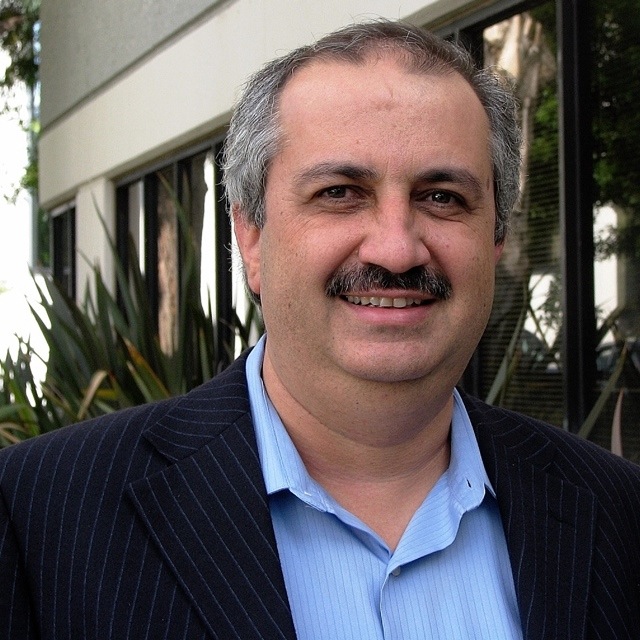
Q&A with photonics pioneer, Richard Soref - Part 1
Richard Soref has spent over 50 years researching photonics, contributing groundbreaking work in the areas of liquid crystals, silicon photonics and the broader topic of mid-infrared wavelengths and Group IV photonics. For 27 years he was employed at the Air Force Research Laboratory. He has also worked at the Sperry Research Center, the MIT Lincoln Laboratory, and is now a research professor at the University of Massachusetts in Boston.
In part 1 of a two-part interview with Gazettabyte, he details his research interests, explains what is meant by Group IV photonics, and discusses why photonics has not matched the semiconductor industry in terms of integration, and how that could change.
Optics is a seemingly small subset of physics but really optics is a huge field with a deep, variegated nature waiting to be discovered
Richard Soref
Q: Having gained your Ph.D. in 1963, you have spent your career in what you call the science of light. What is it about photonics that you find so captivating?
RS: I’ve been drawn to its diversity and classical beauty. Photonics used to be called optics until it was re-labelled by the OSA. Optics is a seemingly small subset of physics but really optics is a huge field with a deep, variegated nature waiting to be discovered. To make progress, you need multiple disciplines, and I’ve always been captivated by the materials science aspect that opens the door to new physics and new devices.
Can you outline your career and how you ended up as a research professor at the University of Massachusetts at Boston?
RS: A general outline is that I chose employers who would encourage exploration of new avenues, would give me freedom to fly or fall – and both are built into research. Basic research is where my talents and passion align. And it helps to be obsessive.
In the early years, I worked mostly alone. Then the pleasures of collaboration became important, and for decades I have been fortunate to have outstanding research partners who did heavy lifting of things like quantum mechanics and electromagnetic modelling.
At Lincoln Lab, I continued the nonlinear optical studies that I began during my Stanford Ph.D. work. Sperry Research was an excellent environment until it fell victim to the corporate research shutdown contagion. Ironically or prophetically, impurity-doped silicon infrared sensors were an early focus at Sperry.
Lithium niobate sparked my 40-year interest in electro-optics: Pockels [effect], Kerr [electro-optic effect], Franz-Keldysh [effect] and more. My extensive work on liquid crystals gained a lot of traction, and at an Information Display show I met scientists from South Korea who told me that my early papers helped them with their commercial flat-panel TV products. It was fulfilling to hear that.
Apart from some governmental distractions, the Air Force Research Laboratory (AFRL) years were a happy time and I welcomed the support of the Air Force Office of Scientific Research (AFOSR); the AFOSR is a national treasure.
Fibre-optic telecom emerged in 1985 when I was at AFRL. The fibres needed semiconductor assistance, I felt. That’s when the new silicon insights came to me. I’m glad that I was able in 1989 to identify silicon-on-insulator (SOI) as the primary waveguided-network platform, and I’m gratified that brilliant and innovative research groups around the world entered this field early on. They strived successfully to perfect this technology. To do my part, I tried to surround the problem in a 1985-2015 series of papers, among them my 1991 silicon-germanium-tin (SiGeSn) direct-gap prediction and my 1992 opto-electronic integrated circuit (OEIC) proposal. My most-cited work is a 1987 paper on free-carrier electro-optics.
Summarising, I had two visions at AFRL: Group IV photonics and long-wave integrated optoelectronics, where long wave denotes anything from two to 200 microns, although the mid-infrared wavelengths are key because of their room temperature possibilities. Perhaps there is a third vision: the multi-technology 3D chip on which seven technologies including bio-chemical could be combined.
Sadly those creative years drew to a close when the Massachusetts laboratory was shut down by the Air Force and the party moved to Wright Patterson AFB in Ohio. At that point, I joined the University of Massachusetts in Boston to stay near family and to keep the technical flame alive in research. I’m still collaborating with wonderful people, most of them young.
Can you provide rigour regarding some definitions? Starting with silicon photonics, silicon mid-infrared optics and Group IV photonics, can you define each and do you have a preference for a particular term?
RS: The silicon-photonics term is strongly entrenched in the global community. The phrase includes on-chip germanium photo-detectors and presumably germanium lasers. Nevertheless, I think this term is a bit narrow or misleading about the silicon-germanium-tin materials (SiGeSn) that likely will be used in the monolithic silicon chip of the future.
I am in the minority when I say that I prefer the wider term Group IV photonics (GFP) which takes into account those three-part alloys as well as diamond and graphene. This GFP term was coined in 2003 in my office at Hanscom when Greg Sun and I were dreaming constructively about a new, dedicated IEEE conference, the international meeting I co-founded in 2004.
In the coming years, the purely photonic integrated circuit, the PIC chip, will evolve, after money is spent, into the opto-electronic chip, and the transistors will be CMOS or BiCMOS or heterojunction bipolar
What about the OEIC, how does it differ from silicon photonics? And lastly, nano-photonics, how does it compare to silicon photonics?
RS: The opto-electronic integrated circuit describes the synergistic marriage of nano-photonics and nano-electronics on the same silicon chip. Others have called this an electronic-photonic integrated circuit or EPIC. In essence, the OEIC is a transistorised photonic chip containing electronic intelligence, signal processing, computation, electrical control of active photonic devices, and perhaps RF wireless transceiving capability, which I strongly advocate.
In the coming years, the purely photonic integrated circuit, the PIC chip, will evolve, after money is spent, into the opto-electronic chip, and the transistors will be CMOS or BiCMOS or heterojunction bipolar. These possibilities illustrate the diversity of GFP.
As for nano-photonics, it is a subset of silicon photonics populated by wave-guided components whose smallest cross-section dimension is 15 to 30 percent of the free-space wavelength. Photonics, like electronics, started as micro and shrank to nano. The term nano means nanometer-scale and applies also to quantum-dot diameter, quantum-well layer thickness and photonic-crystal air hole diameter.
In over half a century, electronics has undergone an extraordinary transformation from simple integrated circuits to profoundly complex ones. Yet while integrated optics was spoken of as early as 1969 in the Bell Labs paper by Stuart Miller, integration has been far more modest. Why?
RS: The main roadblock has been the lack of compelling applications for medium scale and large scale photonic integration. Perhaps this was a lack of vision or a lack of market to drive the integration research.
Another inhibiting factor is the large expense, the cost-per-run of making a photonic integrated circuit, although the OPSIS user foundry [before it closed] and other user facilities have mitigated entry costs to some extent. Additional factors are the area-footprint and volume of the photonic building blocks. The photonic device size is generally larger, or much larger, than the size of the modern individual transistor.
Is this about to change?
RS: To some degree, yes. People are packing photonic components together in a circuit but there are limits on how closely this can be done. These constraints lead me to wonder whether photonic integration will follow the same historical path as micro- and nano-electronics, the same developmental story. Will there be a Moore’s law for photonics with PIC packing density doubling every 18 months? The billion-photonic circuit is not on the cards, so I doubt that the law will hold.
The diffraction limit of optics and the single-mode criteria set lower limits on photonic size, although plasmonic devices go below those dimensional limits and are compatible with photonics.
I see glimmers today of where LSI can make a difference. A near-term use is a 128x128 array of electro-optical phase shifters for optical beam steering. More speculatively, we have electro-optical logic arrays, spectrometers on-chip, optical neural networks, dense wavelength-division multiplexers and demultiplexers, quantum processors, and optical computers using dense nano-LED arrays.
The government has deeper pockets than industry for sustained R&D efforts
What are the major challenges today making optical devices using a CMOS fabrication process?
RS: A partially-met challenge is to actualise a stable and reliable process in a 130nm or 65nm CMOS node for manufacturing the active and passive photonic parts of the on-chip network. We need process procedures for principal components which are recipes defined with a new design library. Whether to standardise photonics is an open question. When and where to place transistor circuits on-chip is a challenge. Putting transistors on a separate chip is a near-term alternative.
It takes art as well as science to determine the opto-electronic layering and to decide whether the available processing temperatures necessitate fabrication at the front end or back end of the overall process.
I believe that a manufacturing initiative is an essential next step for GFP to convince friends and skeptics alike of the long-term commercial and military value of GFP offered in new generations of energy-efficient ultra-performance chipsets. The government has deeper pockets than industry for sustained R&D efforts, so I believe that the Department of Defense can be the force driving GFP expansion into higher realms at very low costs per chip.
That’s why I welcome the new 5-year Integrated Photonics Institute project as part of the National Network for Manufacturing Innovation, funded by the RAMI bill [Revitalize American Manufacturing and Innovation Act]. It is a bill that would train the workforce, while public-private partnerships will transform research into products and will deploy infrastructure that supports US-enterprise competitiveness.
For the second part, click here
Graphene prototype modulator shown working at 10 Gigabit
- Imec's graphene electro-absorption modulator works at 10 Gigabit-per-second
- The modulator is small and has be shown to be thermally stable
- Much work is required to develop the modulator commercially
 Cross-section of the graphene electro-absorption modulator. The imec work was first detailed in a paper at the IEDM conference held in December 2014 in San Francisco. Source: imec
Imec has demonstrated an optical modulator using graphene operating at up to 10 Gigabit. The Belgium nano-electronics centre is exploring graphene - carbon atoms linked in a 2D sheet - as part of its silicon photonics research programme investigating next-generation optical interconnect. Chinese vendor Huawei joined imec's research programme late last year.
Several characteristics are sought for a modulator design. One is tiny dimensions to cram multiple interfaces in as tight a space as possible, as required for emerging board-to-board and chip-to-chip optical designs. Other desirable modulator characteristics include low power consumption, athermal operation, the ability to operate over a wide range of wavelengths, high speed (up to 50 Gbps) and ease of manufacture.
Imec's interest in graphene stems from the material's ability to change its light-absorbing characteristics over a wide spectral range. "Graphene has a high potential for a wide-band modulator solution and also for an athermal design," says Joris Van Campenhout, programme director for optical I/O at imec.
 Source: Gazettabyte
Modulation
For optical modulation, either a material's absorption coefficient or its refractive index is used. Silicon photonics has already been used to implement Mach-Zehnder interferometer and ring resonator modulators. These designs modifying their refractive index and use interference to induce light intensity modulation.
"Mach-Zehnder modulators have been optimised dramatically over the last decade," says Van Campenhout. "They can generate at very high bit rates but they are still pretty big - 1mm or longer - and that prevents further scaling."
Ring resonators are more compact and have been shown working at up to 50 Gigabit. "But they are resonant devices; they are wavelength-specific and thermally dependent," says Van Campenhout. "A one degree change can detune the ring resonance from the laser's wavelength."
The other approach, an electro-absorption modulator, uses an electric field to vary the absorption coefficient of the material and this is the graphene modulator approach imec has chosen.
Electro-absorption modulators using silicon germanium meet the small footprint requirement, have a small capacitance and achieve broadband operation. Capacitance is an important metric as it defines the modulator's maximum data rate as well as such parameters as insertion loss (how many dBs of signal are lost passing through the modulator) and the extinction ratio (a measure of the modulator's on and off intensity).
"Silicon germanium offers a pretty decent modulation quality," says Van Campenhout but the wavelength drifts with temperature. Thermal drift is something that graphene appears to solve.
Imec's graphene electro-absorption modulator comprises a 50 micron graphene-oxide-silicon capacitor structure residing above a silicon-on-insulator rib waveguide. The waveguides are implemented using a 200mm wafer whereas the graphene is grown on a copper substrate before being placed on the silicon die. Van Campenhout refers to the design as hybrid or heterogenous silicon photonics.
The graphene modulator exhibits a low 4dB insertion loss and an extinction ratio of 2.5dB. The device's performance is stable over a broad spectrum: an 80nm window centred around the 1550nm wavelength. The performance of up to 10Gbps was achieved over a temperature range of 20-49°C.
"The key achievement is that we have been able to show that you can operate at 10 Gigabit with very clean modulation eye diagrams," says Van Campenhout. However, much work is needed before the device becomes a viable technology.
 Source: Gazettabyte, imec
What next?
Imec has modelled the graphene modulator using a simple resistor-capacitor circuit. "We have been able to identify sources of capacitance and resistance," says Van Campenhout. "We can now better optimise the design for speed or for efficiency."
The speed of the modulator is dictated by the resistance-capacitance product. Yet the higher the capacitance, the greater the efficiency: the better the extinction ratio and the lower the insertion loss. "So it comes down to reducing the resistance," says Van Campenhout. "We think we should be able to get to 25 Gigabit."
With the first prototype, the absorption effect induced by the electric field is achieved between a single graphene plate and the silicon. Imec plans to develop a design using two graphene plates. "If two slabs of graphene are used, we expect to double the effect," says Van Campenhout. "All the charge on both plates of the capacitor will contribute to the modulation of the absorption."
However the integration is more difficult with two plates, and two metal contacts to graphene are needed. "This is still a challenge to do," says Van Campenhout.
Imec has also joined the Graphene Flagship, the European €1 billion programme that spans materials production, components and systems. "One of the work packages is to show you can process on a manufacturing scale graphene-based devices in a CMOS pilot line," he says. Another consideration is to use silicon nitride waveguides rather than silicon ones as these can be more easily deposited.
One challenge still to be overcome is the development of an efficient graphene-based photo-detector. "If this technology is ever going to be used in a real application, there should be a much more efficient graphene photo-detector being developed," says Van Campenhout.
Silicon photonics: Q&A with Kotura's CTO
A Q&A with Mehdi Asghari, CTO of silicon photonics start-up, Kotura. In part one, Asghari talks about a recent IEEE conference he co-chaired that included silicon photonics, the next Ethernet standard, and the merits of silicon photonics for system design.
Part 1
"Photons and electrons are like cats and dogs. Electrons are dogs: they behave, they stick by you, they are loyal, they do exactly as you tell them, whereas cats are their own animals and they do what they like. And that is what photons are like."
Mehdi Asghari, CTO of Kotura
Q: You recently co-chaired the IEEE International Conference on Group IV Photonics that included silicon photonics. What developments and trends would you highlight?
A: This year I wanted to show that silicon photonics was ready to make a leap from an active area of scientific research to a platform for engineering innovation and product development.
To this end, I needed to show that the ecosystem was ready and present. Therefore, a key objective was to get the industry more involved with the conference. "This has always been a challenge," I was told.
To address this issue I asked my co-chair, MIT's Professor Jurgen Michel, that we appoint joint-session chairs, one from industry and one from academia. We got people we knew from Google, Oracle and Intel as co-chairs, and paired them with prominent academics and asked them to ensure that there were an equal number of industry-invited talks in the schedule. We knew this would be a major attraction to industry attendees. We also got the industry to fund the conference at a level that set an IEEE record.
A key highlight of the show was a boat cruise journey on San Diego bay with Dr. Andrew Rickman as speaker, sharing his experiences and thoughts about setting up the first silicon photonics company - Bookham Technology - over 20 years ago.
Among other distinguished industry speakers we had Samsung telling us of the role of silicon photonics in consumer applications, Broadcom on the need for on-chip optical communication, Cisco on the role of silicon photonics in the future of the Internet, and Google on its broadband fibre-to-the-home (FTTh) initiative and what silicon photonics could offer in this area.
Oracle also shared its latest development in silicon photonics and the application of the technology in their systems, while Luxtera discussed the latest developments in its CMOS photonics platform, particularly the 4x25 Gigabit-per-second (Gbps) platform.
We also heard about the latest germanium laser development at MIT and had an invited speaker to talk about what III-V devices could do and to provide a comparison to silicon to make sure we are not blinded by our own rhetoric.
We ended up with a record number of attendees for the conference and, perhaps more importantly, close to half from industry; a record and vindicated my motivation and perspective for the conference and that silicon photonics is ready and coming.
Was there a trend or presentation at the IEEE event that stood out?
There are two areas creating excitement. One is the germanium laser. This is a topic of significant interest because these devices can operate at very high temperatures and therefore they can be next to the processor or ASIC. This can be a game-changer in how we envisage photonics and electronics being integrated.
We have germanium detectors and at Kotura we are working very hard to get a germanium electro-absorption modulator. We have shown this device can be extremely small and low power. And it can operate at very high speed - we have observed 3dB bandwidths in excess of 70GHz which means you can think of 100 Gigabit direct modulation for a device only 40 microns long and with a capacitance of a few femtofarads. So in terms of RF power, the dissipation of this device is virtually zero.
I would say the MIT group is probably leading the [germanium laser] efforts. They reported on room-temperature, current-driven laser emission which is very exciting. The efficiency of these lasers are still low for commercial applications; they probably have to improve by a factor of 100 or so. But given the progress we've seen in the last two years, if they keep going at that pace we may have viable germanium lasers in a couple of years. Then someone in industry has to take that on and turn it into a product and that is usually the hardest part.
This is exciting because that enables us to forget about off-the-chip lasers and integrate them in the device. We can then give up a whole bunch of problems. For example, the high temperature operation of the III-V devices is a real limit for us. Electronic devices can give off 100W and operate at 120oC, whereas optical devices often have to be stabilised, may go through multiple packaging layers, and the heat dissipation is usually directly related to cost.
If you could end up with a germanium laser that is happy at high temperatures - and we know our detectors and modulators work at high temperatures, and we know we can use electronic packaging to package these devices - then we can put these lasers next to the processor and address the bandwidth limitations that ASICs are facing today.
"Wavelength division multiplexing (WDM) is effectively a zero-power gearbox"
What was the second area?
The other area that was very interesting is graphene, a new material people are starting to work with and putting on silicon. They [researchers] are showing very low power, very high speed operation. It is still at a research level but that is another area we should watch.
The IEEE has started a group looking at the next speed Ethernet standard. No technical specification has been mentioned but it looks that 400 Gigabit Ethernet (GbE) will be the approach. Do you agree and what role can silicon photonics play in making the next speed Ethernet standard possible?
Industry is busy arguing about the different ways of doing 100 and 400GbE, and perhaps forgetting the fact that we have been here before.
The simple fact is that people always go for higher bit rate when it is cost-efficient and power-efficient to do so. After that, wavelengths are used.
Wavelength division multiplexing (WDM) is effectively a zero-power 'gearbox', mixing the signals in the optical domain. You do pay a power penalty for it in the form of photons lost in the multiplexer and demultiplexer. However that is not significant compared to the power consumption of an electronics gearbox chip.
Once we have exploited line rate and wavelength division multiplexing, we come to more complex modulation formats and pay the associated power and complexity penalty. Of course, more channels of fibre can always carry more information bandwidth but that is just a brute force solution that works while density and bandwidth requirements are moderate.
I think the right 100 Gigabit is based on a WDM 4x25 Gig solution. This can then scale to 400 Gigabit by adding more wavelengths, and can then scale to 1.6 Terabits. We have already demonstrated this in a single chip and will demonstrate this later in the form of a QSFP 100Gbps.
How does the interface scale to 1.6Tbps?
Our devices are capable of running at 40 or 50Gbps, depending on the electronics. The electronics is going to limit the speed of our devices. We can very easily see going from four channels at 25Gbps to 16 channels at 25Gbps to provide a 400 Gigabit solution.
We can also see a way of increasing the line rate to 50Gbps perhaps, either a straightforward NRZ (non-return-to-zero) line rate or some people are talking about multi-level modulation, PAM-4 (pulse amplitude modulation) type of stuff, to get to 50Gbps.
The customers we are talking to about 100Gbps are already talking about 400Gbps. So we can see 16x25Gbps, or 8x50Gbps if that is the right thing to do at the time based on the availability of electronics.
To go to 1.6 Terabit transceivers, we envisage something running at 40Gbps times 40 channels or 50Gbps times 32 channels. We already have done a single receiver chip demonstrator that has 40 channels, each at 40Gbps.
These things in silicon are not a big deal. The III-V guys really struggle with yield and cost. But you can envisage scaling to that level of complexity in a silicon platform.
Silicon photonics is spoken of not just as an optical platform like traditional optical integration technologies, but also as a design approach, making use of techniques associated with semiconductor design. The implication is that the technology will enable designs and even systems in a way that traditional optics can't. Can you explain how silicon photonics is a design approach and just what the implications are?
I think this is a key promise of silicon photonics, but perhaps one that has been oversold in recent years.
The key here is that given the maturity of the silicon processing capabilities, process simulation tools available and inherent properties of silicon, it is possible to predict the performance of the optical circuits far better in this platform than in any other before it. I think this is true and very valuable, potentially even a game changer.
However, we have to realise that there still remains an inherent difference between electrons and photons and their behavior in such circuits. Photons remain in a quantum world in such circuits, where the wavelength of light is comparable to feature sizes we manufacture. Hence we are dealing with a statistical quantum process whether we like it or not.
In summary, silicon will be a key enabler for on-chip system design, but it is too early for the university courses to stop graduating photonics PhDs!
So there is an advantage to silicon photonics but are you saying it is not that simple as using mature semiconductor design techniques?
Photons and electrons are like cats and dogs. Electrons are dogs: they behave, they stick by you, they are loyal, they do exactly as you tell them, whereas cats are their own animals and they do what they like. And that is what photons are like.
So it is really hard to predict what a photon does. The dimensions that we use for the structures we make are of the size of the wavelength of a photon. And that means it is more of a hit-and-miss process - there is always stray light, the stray light has a habit of interfering and you can always get unpredicted results.
When I interact with my electronic partners I find that they go through 6-9 months of very detailed simulation. They have very complex simulation tools.
When you come to photonics for sure we can borrow some of these simulation tools, we can simulate the process because we are using silicon. However some of the tolerances that we need are beyond what the silicon guys need, and the way the photons behave is very different. So in the end we don't spend 9 months simulating; we spend a month simulating and 3 months running the process and optimising it and re-running it and re-optimising it.
We end up with a reverse situation where the design is only 3 months, and the interaction with the designer and the manufacturing process is a 9-month process. So this is more of an iterative process. It is not as mature and a little bit more statistical.
OFC/NFOEC 2012: Technical paper highlights
 Source: The Optical Society
Novel technologies, operators' experiences with state-of-the-art optical deployments and technical papers on topics such as next-generation PON and 400 Gigabit and 1 Terabit optical transmission are some of the highlights of the upcoming OFC/NFOEC conference and exhibition, to be held in Los Angeles from March 4-8, 2012. Here is a taste of some of the technical paper highlights.
Optical networking
In Spectrum, Cost and Energy Efficiency in Fixed-Grid and Flew-Grid Networks (Paper number 1248601) an evaluation of single and multi-carrier networks at rates up to 400 Gigabit-per-second (Gbps) is made by the Athens Information Technology Center. One finding is that efficient spectrum utilisation and fine bit-rate granularity are essential if cost and energy efficiencies are to be realised.
In several invited papers, operators report their experiences with the latest networking technologies. AT&T Labs discusses advanced ROADM networks; NTT details the digital signal processing (DSP) aspects of 100Gbps DWDM systems and, in a separate paper, the challenge for Optical Transport Network (OTN) at 400Gbps and beyond, while Verizon gives an update on the status of MPLS-TP. As part of the invited papers, Finisar's Chris Cole outlines the next-generation CFP modules.
Optical access
Fabrice Bourgart of FT-Orange Labs details where the next generation PON standards - NGPON2 - are going while NeoPhotonics's David Piehler outlines the state of photonic integrated circuit (PIC) technologies for PONS. This is also a topic tackled by Oclaro's Michael Wale: PICs for next-generation optical access systems. Meanwhile Ao Zhang of Fiberhome Telecommunication Technologies discusses the state of FTTH deployments in the world's biggest market, China.
Switching, filtering and interconnect optical devices
NTT has a paper that details a flexible format modulator using a hybrid design based on a planar lightwave circuit (PLC) and lithium niobate. In a separate paper, NTT discusses silica-based PLC transponder aggregators for a colourless, directionless and contentionless ROADM, while Nistica's Tom Strasser discusses gridless ROADMs. Compact thin-film polymer modulators for telecoms is a subject tackled by GigOptix's Raluca Dinu.
One novel paper is on graphene-based optical modulators by Ming Liu, Xiang at the UC Berkeley (Paper Number: 1249064). The optical loss of graphene can be tuned by shifting its Fermi level, he says. The paper shows that such tuning can be used for a high-speed optical modulator at telecom wavelengths.
Optoelectronic Devices
CMOS photonic integrated circuits is the topic discussed by MIT's Rajeev Ram, who outlines a system-on-chip with photonic input and output. Applications range from multiprocessor interconnects to coherent communications (Paper Number: 1249068).
A polarisation-diversity coherent receiver on polymer PLC for QPSK and QAM signals is presented by Thomas Richter of the Fraunhofer Institute for Telecommunications (Paper Number: 1249427). The device has been tested in systems using 16-QAM and QPSK modulation up to 112 Gbps.
Core network
Ciena's Maurice O'Sullivan outlines 400Gbps/ 1Tbps high-spectral efficiency technology and some of the enabling subsystems. Alcatel-Lucent's Steven Korotky discusses traffic trends: drivers and measures of cost-effective and energy-efficient technologies and architectures for the optical backbone networks, while transport requirements for next-generation heterogeneous networks is the subject tackled by Bruce Nelson of Juniper Networks.
Data centre
IBM's Casimir DeCusatis presents a future - 2015-and-beyond - view of data centre optical networking. The data centre is also tackled by HP's Moray McLaren, in his paper on future computing architectures enabled by optical and nanophotonic interconnects. Optically-interconnected data centres are also discussed by Lei Xu of NEC Labs America.
Expanding usable capacity of fibre syposium
There is a special symposium at OFC/ NFOEC entitled Enabling Technologies for Fiber Capacities Beyond 100 Terabits/second. The papers in the symposium discuss MIMO and OFDM, technologies more commonly encountered in the wireless world.