
Drut tackles disaggregation at a data centre scale
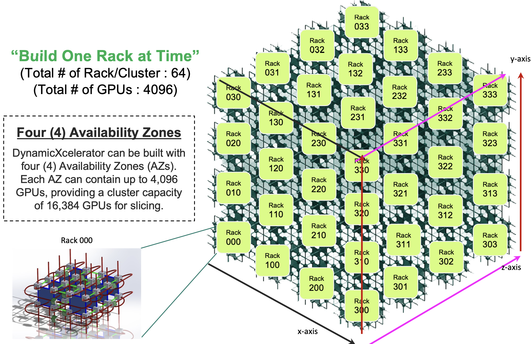
- Drut’s DynamicXcelerator supports up to 4,096 accelerators using optical switching and co-packaged optics. Four such clusters enable the scaling to reach 16,384 accelerators.
- The system costs less and is cheaper to run, has lower latency, and better uses the processors and memory.
- The system is an open design supporting CPUs and GPUs from different vendors.
- DynamicXcelerator will ship in the second half of 2024.
Drut Technologies has detailed a system that links up to 4,096 accelerator chips. And further scaling, to 16,384 GPUs, is possible by combining four such systems in ‘availability zones’.
The US start-up previously detailed how its design can disaggregate servers, matching the processors, accelerators, and memory to the computing task at hand. Unveiled last year, the product comprises management software, an optical switch, and an interface card that implements the PCI Express (PCIe) protocol over optics.
The product disaggregates the servers but leaves intact the tiered Ethernet switches used for networking servers across a data centre.
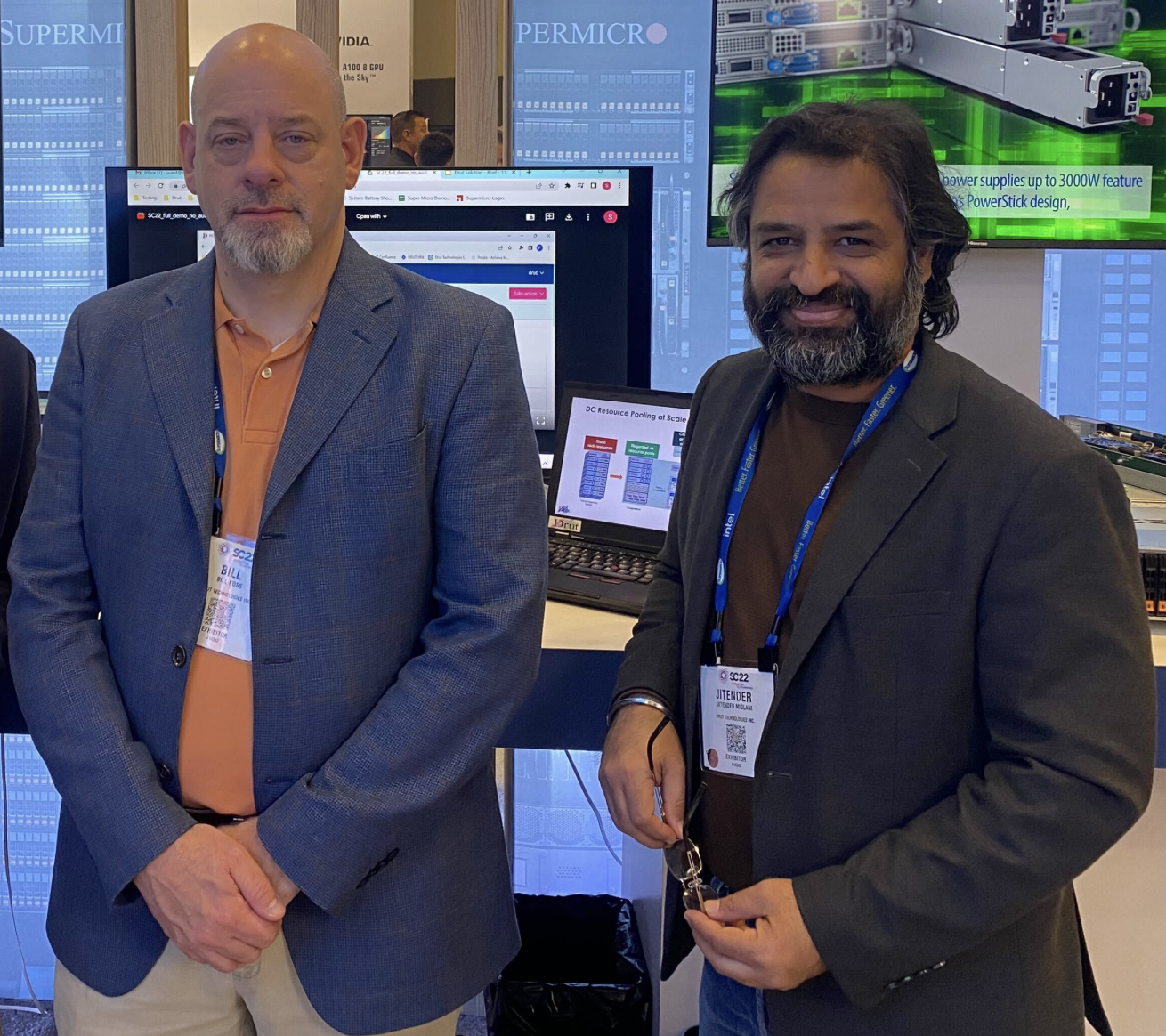
Now the system start-up is expanding its portfolio with a product that replaces the Ethernet switches with optical ones. “You can compose [compute] nodes and drive them using our software,” says Bill Koss, CEO of Drut.
Only Google has demonstrated the know-how to make such a large-scale flexible computing architecture using optical switching.
Company background
Drut was founded in 2018 and has raised several funding rounds since 2021.
Jitender Miglani, founder and president of Drut, previously worked at MEMS-based optical switch maker, Calient Technologies.
Drut’s goal was to build on its optical switching expertise and add the components needed to make a flexible, disaggregated computing architecture. “The aim was building the ecosystem around optical switches,” says Miglani.
The company spent its first two years porting the PCIe protocol onto an FPGA for a prototype interface card. Drut showcased its prototype product alongside a third-party optical switch as part of a SuperMicro server rack at the Supercomputing show in late 2022.
Drut has spent 2023 developing its next-generation architecture to support clusters of up to 4,096 endpoints. These can be accelerators like graphics processing units (GPUs), FPGAs, data processing units (DPUs), or storage using the NVM Express (nonvolatile memory express).
The architecture, dubbed DynamicXcelerator, supports PCIe over optics to link processors (CPUs and GPUs) and RDMA (Remote Direct Memory Access) over optics for data communications between the GPUs and between the CPUs.
The result is the DynamicXcelerator system, a large-scale reconfigurable computing for intensive AI model training and high-performance computing workloads.
DynamicXcelerator
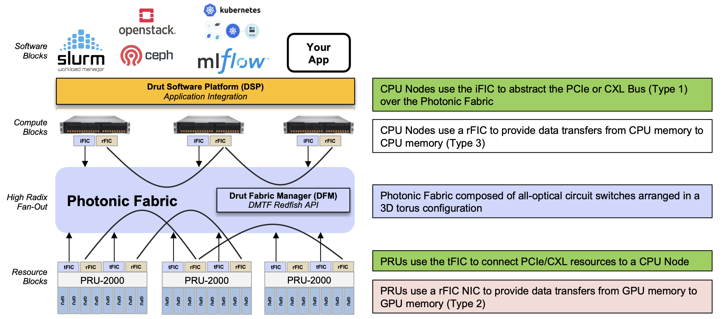
The core of the DynamicXcelerator architecture is a photonic fabric based on optical switches. This explains why Drut uses PCIe and RDMA protocols over optics.
Optical switches brings size and flexibility and by relaying optical signals, their ports are data-rate independent.
Another benefit of optical switching is power savings. Drut says an optical switch consumes 150W whereas an equivalent-sized packet switch consumes 1,700W. On average, an Infiniband or Ethernet packet switch draws 750W when used with passive cables. Using active cables, the switch’s maximum power rises to 1,700W. “[In contrast], a 32-64-128-144 port all-optical switch draws 65-150W,” says Koss.
Drut also uses two hardware platforms. One is the PCIe Resource Unit, dubbed the PRU-2000, which hosts eight accelerator chips such as GPUs. Unlike Nvidia’s DGX platform, which uses Nvidia GPUs such as the Hopper, or Google, which uses its TPU5 tensor processor unit (TPU), Drut’s PRU-2000 is an open architecture and can use GPUs from Nvidia, AMD, Intel, and others. The second class of platform is the compute node or server, which hosts the CPUs.
DynamicXcelerator’s third principal component are the FIC 2500 interface cards.
The iFIC 2500 card is similar to Drut’s current product’s iFIC 1000, which features an FPGA and four QSFP28s. However, the iFIC 2500 supports the PCIe 5.0 generation bus and the Compute Express Link (CXL) protocols. The two other FIC cards are the tFIC 2500 and rFIC 2500.
“The iFIC and tFIC are the same card, but different software images,” says Koss. “The iFIC fits into a compute node or server while the tFIC fits into our Photonic Resource Unit (PRU) unit, which holds GPUs, FPGAs, DPUs, NVMe, and the like.”
The rFIC provides RDMA over photonics for GPU-to-GPU memory sharing. The rFIC card for CPU-to-CPU memory transfers is due later in 2024.
Miglani explains that PCIe is used to connect the GPUs and CPUs, but for GPU-to-GPU communication, RDMA is used since even PCIe over photonics has limitations.
Certain applications will use hundreds and even thousands of accelerators, so a PCIe lane count is one limitation, distance is another; a 5ns delay is added for each metre of fibre. “There is a window where the PCIe specification starts to fall off,” says Miglani.
The final component is DynamicXcelerator’s software. There are two software systems: the Drut fabric manager (DFM), which controls the system’s hardware configuration and traffic flows, and the Drut software platform (DSP) that interfaces applications onto the architecture.
Co-packaged optics
Drut knew it would need to upgrade the iFIC 1000 card. DynamicXcelerator uses PCIe 5.0, each lane being 32 gigabit-per-second (Gbps). Since 16 lanes are used, that equates to 512 gigabits of bandwidth.
“That’s a lot of bandwidth, way more that you can crank out with four 100-gigabit pluggables,” says Koss, who revealed co-packaged optics will replace pluggable modules for the iFIC 2500 and tFIC 2500 cards.
The card for the iFIC and tFIC will use two co-packaged optical engines, each 8×100 gigabits. The total bandwidth of 1.6 terabits – 16×100-gigabit channels – is a fourfold increase over the iFIC 1000.
System workings
The system’s networking can be viewed as a combination of circuit switching and packet switching.
The photonic fabric, implemented as a 3D torus (see diagram), supports circuit switching. Using a 3D torus, three hops at most are needed to link any two of the system’s endpoints.
One characteristic of machine learning training, such as large language models, is that traffic patterns are predictable. This suits an architecture that can set the resources and the connectivity for a task’s duration.
Packet switching is not performed using Infiniband. Nor is a traditional spine-leaf Ethernet switch architecture used. The DynamicXcelerator does uses Ethernet but in the form of a small, distributed switching layer supported in each interface card’s FPGA.
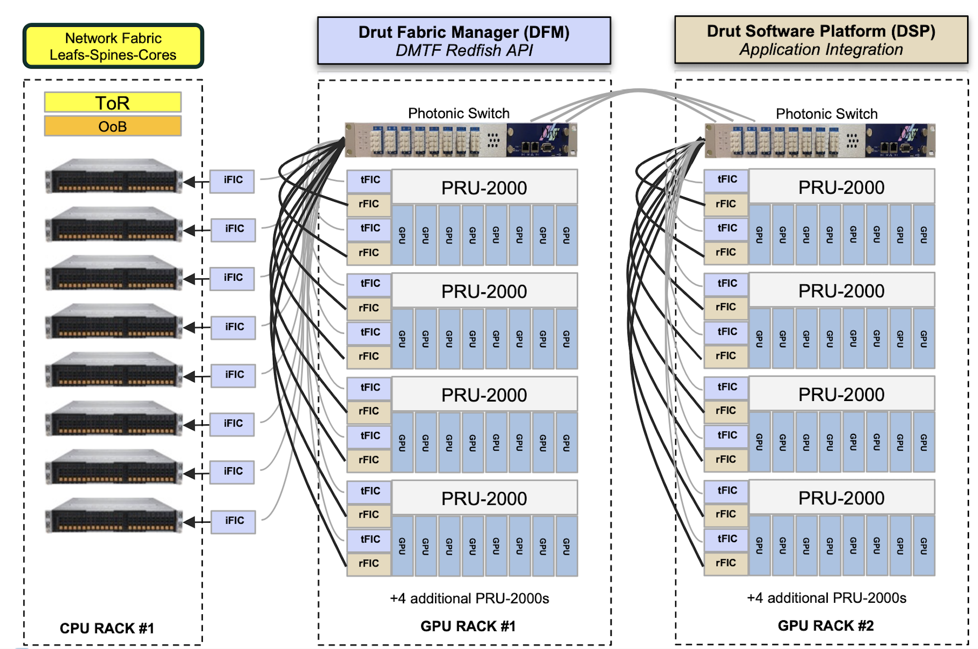
The smallest-sized DynamicXcelerator would use two racks of stacked PRU-2000s (see diagram). Further racks would be added to expand the system.
“The idea is that you can take a very large construct of things and create virtual PODs,” says Koss. “All of a sudden, you have flexible and fluid resources.”
Koss says a system can scale to 16,384 units by combining four clusters, each of 4,096 accelerators. “Each one can be designated as an ‘availability zone’, with users able to call resources in the different zones,” he says.
Customers might use such a configuration to segment users, run different AI models, or for security reasons. “It [a 16,384 unit system] would be huge and most likely something that only a service provider would do or maybe a government agency,” says Koss.
Capital and operation savings
Drut claims the architecture costs 30 per cent less than conventional systems, while operational cost-savings are 40 per cent.
The numbers need explaining, says Koss, given the many factors and choices possible.
The bill of materials of a 16, 32, 64 or 128-GPU design has a 10-30 per cent saving solely from the interconnect.
“The bigger the fabric, the better we scale in price as solutions using tiered leaf-spine-core packet switches involving Ethernet-Infiniband-PCIe are all built around the serdes of the switch chip in the box,” says Koss. “We have a direct-connect fabric with a very high radix, which allows us to build the fabric without stacked tiers like legacy point-to-point networks.”
There are also the power savings, as mentioned. Less power means less heat and hence less cooling.
“We can also change the physical wires in the network,” says Koss, something that can’t be done with leaf-spine-core networks, unless data centre staff change the cabling.
“By grouping resources around a workload, utilisation and performance are much better,” says Koss. “Apps run faster, infrastructure is grouped around workloads, giving users the power to do more with less.”
The system’s evolution is another consideration. A user can upgrade resources because of server disaggregation and the ability to add and remove resources from active machines.
“Imagine that you bought the DynamicXcelerator in 2024. Maybe it was a small sized, four-to-six rack system of GPUs, NVMe, etc,” says Koss. If, in mid-2026, Nvidia releases a new GPU, the user can take several PRU-2000s offline and replace the existing GPUs with the new ones.
“Also if you are an Nvidia shop but want to use the new Mi300 from AMD, no problem,” says Koss. “You can mix GPU vendors with the DynamicXcelerator.” This is different from today’s experience, where what is built is wasteful, expensive, complex, and certainly not climate-conscious, says Koss.
Plans for 2024
Drut has 31 employees, 27 of which are engineers. “We are going on a hiring binge and likely will at least double the company in 2024,” says Koss. “We are hiring in engineering, sales, marketing, and operations.”
Proof-of-concept DynamicXcelerator hardware will be available in the first half of 2024, with general availability then following.

Drut's agile optical fabric for the data centre
A US start-up has developed a photonic fabric for the data centre that pulls together the hardware needed for a computational task.
Drut Technologies offers management software and a custom line card, which, when coupled with the optical switch, grabs the hardware required for the workload.
“You can have a server with lots of resource machines: lots of graphic processing units (GPUs) and lots of memory,” says Bill Koss, CEO of Drut. “You create a machine, attach a workload to it and run it; forever, for a day, or 15 minutes.”
Drut first showcased its technology supporting the PCI Express (PCIe) bus over photonics at server specialist, SuperMicro’s exhibition stand, at the Supercomputing 22 show held last November in Dallas, Texas.
“This is a fully reconfigurable, direct-connect optical fabric for the data centre,” says Koss.
Drut says hyperscalers use between 40 and 60 per cent of the hardware in their data centres. With direct connectivity, resources can be used as needed and released, improving overall hardware utilisation.
Optical circuit switching
Drut’s system is a second recent example of a company using optics for the data centre to establish reconfigurable photonic paths between endpoints, referred to as optical circuit switching.
Google revealed in August 2022 that it had developed its own MEMS-based optical switch design, which the hyperscaler has used for several years in its data centres.
The optical circuit switches are used instead of the highest tier of Ethernet switches – the spine layer – in Google’s data centres.
Using optical circuit switching reduces networking costs by 30 per cent and power consumption by over 40 per cent. The optical switch layer also enables more efficient and less disruptive upgrading of the server endpoints.
Koss says the difference between its design and Google’s is scale: “Ours is more granular.”
Drut says its solution will enable racks of optically-attached machines, but unlike Google, the optical switching is much closer to the end equipment. Indeed, it is a second fabric independent of the data centre’s tiered Ethernet switches.

Product architecture
The main three elements of Drut’s technology are an FPGA-based line card, the fabric-manager software and a third-party optical switch.
Drut’s line card, the iFIC 1000, has an FPGA and four 100-gigabit transceivers. “That is as much as we can fit on,” says Koss.

The company uses its own transport protocol that runs over the fabric, an ‘out-of-band’ network design.
“You can dynamically attach and detach, and the machine doesn’t go into crazy land,” says Koss.
The fabric manager knows all the ports of the switch and the endpoints and sets up the desired system configurations.
With the fabric management software and the FPGA, the system can configure banks of graphic processing units (GPUs).
Drut has also demonstrated linking memory over its photonic fabric, although this is in development and still unavailable as a product.
Drut says a primary challenge was developing the FPGA that takes the out-of-band signalling off the main bus and supports it over the optical fabric.
A photonic fabric design promises to change the nature of a server. A user will request CPUs, accelerators such as GPUs and FPGAs, and memory, as needed, for each workload.
The merits of using an optical switch include its support for multiple ports, i.e. the switch’s large radix, and its being interface-speed agnostic.
The photonic switch also has a lower latency than switch ICs and simplifies cabling. “It is all single-mode fibre pluggable optics,” says Koss.

Status
Drut is developing a second line card which will use a larger FPGA. Each card generation will expand the number of optical ports to scale the endpoints supported.
The company is also working with a co-packaged optics player on a design for a hyperscaler.
“We use pluggable optics today because co-packaged optics isn’t available,” says Koss.
The advantage of co-packaged optics is that it will increase the port density on each line card and hence the overall scaling.
Koss says that Drut already has two customers: an enterprise and a cloud provider.
Drut, which means ‘high tempo’ in Sanskrit, has so far secured two rounds of funding.
“We did a good-sized seed round in June 2021 and closed a bigger seed extension last September; not an easy task in 2022,” says Koss. “We added Boston Seed Capital and another firm as new investors as well.”
The company has sufficient funding till 2024 and is talking to new investors for a Series A funding round.

Building an AI supercomputer using silicon photonics

- Luminous Computing is betting its future on silicon photonics as an enabler for an artificial intelligence (AI) supercomputer
Silicon photonics is now mature enough to be used to design complete systems.
So says Michael Hochberg (pictured), who has been behind four start-ups including Luxtera and Elenion whose products used the technology. Hochberg has also co-authored a book along with Lukas Chrostowski on silicon photonics design.
In the first phase of silicon photonics, from 2000 to 2010, people wondered whether they could even do a design using the technology.
“Almost everything that was being done had to fit into an existing socket that could be served by some other material system,” says Hochberg.
A decade later it was more the case that sockets couldn’t be served without using silicon photonics. “Silicon photonics had dominated every one of the transceiver verticals that matter: intra data centre, data centre interconnect, metro and long haul,” he says.
Now people have started betting their systems using silicon photonics, says Hochberg, citing the examples as lidar, quantum optics, co-packaged optics and biosensing.
Several months ago Hochberg joined as president of Luminous Computing, a start-up that recently came out of stealth mode after raising $105 million in Series A funding.
Luminous is betting its future on silicon photonics as an enabler for an artificial intelligence (AI) supercomputer that it believes will significantly outperform existing platforms.
Machine learning
The vision of AI is to take tasks that were the exclusively the domain of the human mind and automate them at scale, says Hochberg.
Just in the last decade, the AI community has advanced from doing things using machine learning (ML) that are trivial for humans to tasks that only the most talented experts can achieve.
“We have reached the point where machine learning capabilities are superhuman in many respects,” says Hochberg. “Where they produce results quantifiably better than humans can.”
But achieving such machine learning progress has required huge amounts of data and hardware.
“The training runs for the state-of-the-art recommendation engines and natural language models take tens to hundreds of thousands of GPUs (graphics processing units) and they run from months to years,” says Hochberg.
Moreover, the computational demands associated with machine learning training aren’t just doubling every 18 months, like with Moore’s law, but every 3-4 months. “And for memory demands, it is even faster,” he says.
What that means is that the upper limit for doing such training runs are complete data centres.
Luminous Computing wants to develop AI hardware that scales quickly and simply. And a key element of that will be to use silicon photonics to interconnect the hardware.
“One of the central challenges scaling up big clusters is that you have one kind of bus between your CPU and memory, another between your CPU and GPU, another between the GPUs in a box and yet another – Infiniband – between the boxes,” says Hochberg.
These layers of connectivity run at different speeds and latencies that complicate programming for scale. Such systems also result in expensive hardware like GPUs being under-utilised.
“What we are doing is throwing massive optical interconnect at this problem and we are building the system around this optical interconnect,” says Hochberg.
Using sufficient interconnect will enable the computation to scale and will simplify the software. “It is going to be simple to use our system because if you need anything in memory, you just go and get it because there is bandwidth to spare.”
Supercomputing approach
Luminous is not ready to reveal its supercomputer architecture. But the company says it is vertically integrated and is designing the complete system including the processing and interconnect.
When the company started in 2018, it planned to use a photonic processor as the basis of the compute but the class of problems it could solve were deemed insufficiently impactful.
The company then switched to developing a set of ASICs designed around the capabilities of the optics. And it is the optics that rearchitects how data moves within the supercomputer.
“That is the place where you get order-of-magnitude advantages,” says Hochberg.
The architecture will tackle a variety of AI tasks typically undertaken by hyperscalars. “If we can enable them to run models that are bigger than what can be run today while using much smaller programming teams, that has enormous economic impact,” he says.
Hochberg also points out that many organisations want to use machine learning for lots of markets: “They would love to have the ability to train on very large data sets but they don’t have a big distributed systems engineering team to figure out how to scale things up onto big-scale GPUs; that is a market that we want to help.”
The possible customers of Luminous’s system are so keen to access such technology that they are helping Luminous. “That is something I didn’t experience in the optical transceiver world,” quips Hochberg.
The supercomputer will be modular, says Luminous, but its smallest module will have much greater processing capability than, say, a platform hosting 8 or 16 GPUs.
Silicon photonics
Luminous is confident in using silicon photonics to realise its system even though the design will advance how the technology has been used till now.
“You are always making a bet in this space that you can do something that is more complex than anything anyone else is doing because you are going to ship your product a couple of years hence,” says Hochberg
Luminous is has confidence because of the experience of its design team, the design tools it has developed and its understanding of advanced manufacturing processes.
“We have people that know how to stand up complex things,” says Hochberg.
Status
Luminous’s staff is currently around 100, a doubling in the last year. And it is set to double again by year-end.
The company is busy doing modelling work as to how the machine learning algorithms will run on its system. “Not just today’s models but also tomorrow’s models,” says Hochberg.
Meanwhile, there is a huge amount of work to be done to deliver the first hardware by 2024.
“We have a bunch of big complex chips we have to build, we have software that has to live on top of it, and it all has to come together and work,” concludes Hochberg.

PCI-SIG releases the next PCI Express bus specification

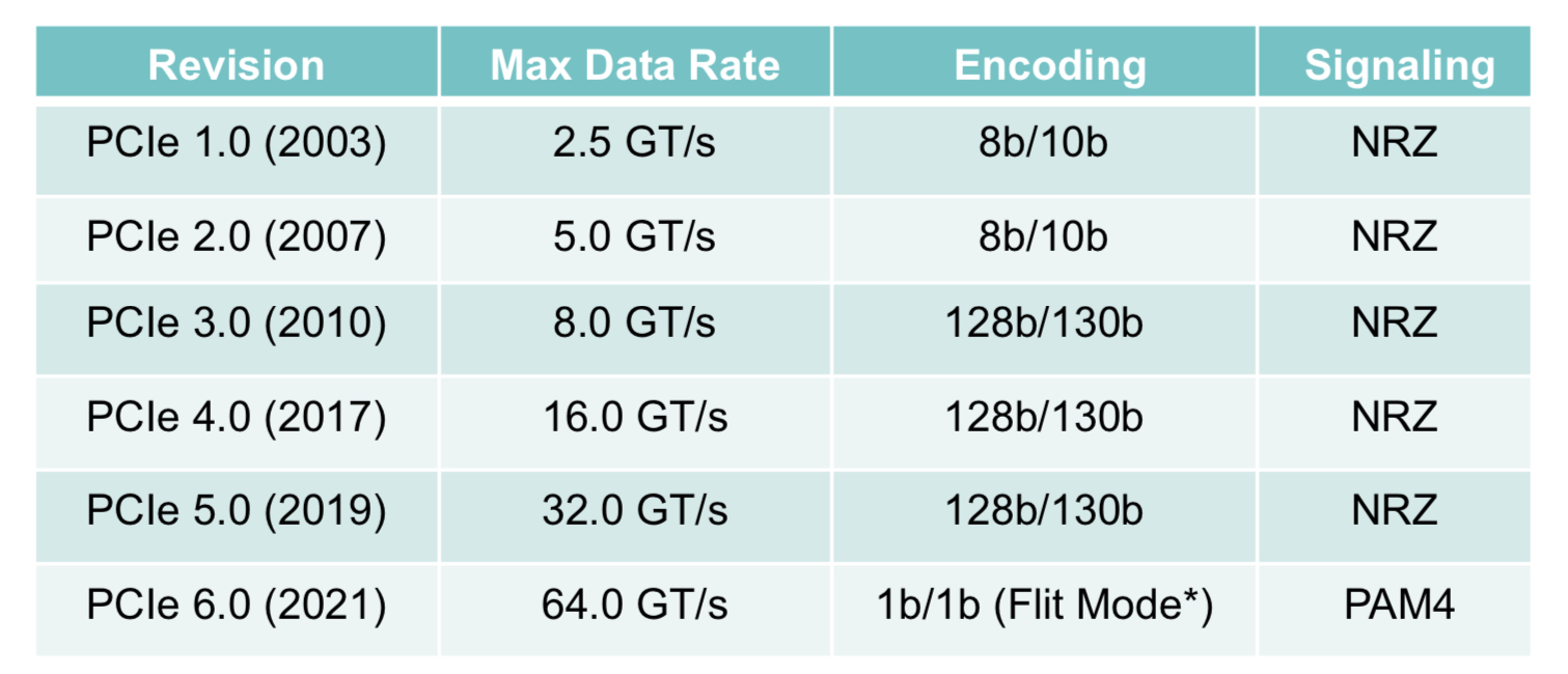
The Peripheral Component Interconnect Express (PCIe) 6.0 specification doubles the data rate to deliver 64 giga-transfers-per-second (GT/s) per lane.
For a 16-lane configuration, the resulting bidirectional data transfer capacity is 256 gigabytes-per-second (GBps).
“We’ve doubled the I/O bandwidth in two and a half years, and the average pace is now under three years,” says Al Yanes, President of the Peripheral Component Interconnect – Special Interest Group (PCI-SIG).
The significance of the specification’s release is that PCI-SIG members can now plan their products.
Users of FPGA-based accelerators, for example, will know that in 12-18 months there will be motherboards running at such rates, says Yanes
Applications
The PCIe bus is used widely for such applications as storage, processors, artificial intelligence (AI), the Internet of Things (IoT), mobile, and automotive.
In servers, PCIe has been adopted for storage and by general-purpose processors and specialist devices such as FPGAs, graphics processor units (GPUs) and AI hardware.
The CXL standard enables server disaggregation by interconnecting processors, accelerator devices, memory, and switching, with the protocol sitting on top of the PCIe physical layer. The NVM Express (NVMe) storage standard similarly uses PCIe.
“If you are on those platforms, you know you have a healthy roadmap; this technology has legs,” says Yanes.
A focus area for PCI-SIG is automotive which accounts for the recent membership growth; the organisation now has 900 members. PCI-SIG has also created a new workgroup addressing automotive.
Yanes attributes the automotive industry’s interest in PCIe due to the need for bandwidth and real-time analysis within cars. Advanced driver assistance systems, for example, use a variety of sensors and technologies such as AI.
PCIe 6.0
The PCIe bus uses a dual simplex scheme – serial transmissions in both directions – referred to as a lane. The bus can be configured in several lane configurations: x1, x2, x4, x8, x12, x16 and x32, although x2, x12 and x32 are rarely used.
PCIe 6.0’s 64GT/s per lane is double that of PCIe 5.0 that is already emerging in ICs and products.
IBM’s latest 7nm POWER10 16-core processor, for example, uses the PCIe 5.0 bus as part of its I/O, while the latest data processing units (DPUs) from Marvell (Octeon 10) and Nvidia (BlueField 3) also support PCIe 5.0.
To achieve the 64GT/s transfer rates, the PCIe bus has adopted 4-level pulse amplitude modulation (PAM-4) signalling. This requires forward error correction (FEC) to offset the bit error rates of PAM-4 while minimising the impact on latency. And low latency is key given the PCIe PHY layer is used by such protocols as CXL that carry coherency and memory traffic. (see IEEE Micro article.)
The latest specification also adopts flow control unit (FLIT) encoding. Here, fixed 256-byte packets are sent: 236 bytes of data and 20 bytes of cyclic redundancy check (CRC).
Using fixed-length packets simplifies the encoding, says Yanes. Since the PCIe 3.0 specification, 128b/130b encoding has been used for clock recovery and the aligning of data. Now with the fixed-sized packet of FLIT, no encoding bits are needed. “They know where the data starts and where it ends,” says Yanes.
Silicon designed for PCIe 6.0 will also be able to use FLITs with earlier standard PCIe transfer speeds.
Yanes says power-saving modes have been added with the release. Both ends of a link can agree to make lanes inactive when they are not being used.
Status and developments
IP blocks for PCIe 6.0 already exist while demonstrations and technology validations will occur this year. First products using PCIe 6.0 will appear in 2023.
Yanes expects PCIe 6.0 to be used first in servers with accelerators used for AI and machine learning, and also where 800 Gigabit Ethernet will be needed.
PCI-SIG is also working to develop new cabling for PCIe 5.0 and PCIe 6.0 for sectors such as automotive. This will aid the technology’s adoption, he says
Meanwhile, work has begun on PCIe 7.0.
“I would be ecstatic if we can double the data rate to 128GT/s in two and a half years,” says Yanes. “We will be investigating that in the next couple of months.”
One challenge with the PCIe standard is that it borrows the underlying technology from telecom and datacom. But the transfer rates it uses are higher than the equivalent rates used in telecom and datacom.
So, while PCI 6.0 has adopted 64GT/s, the equivalent rate used in telecom is 56Gbps only. The same will apply if PCI-SIG chooses 128GT/s as the next data rate given that telecom uses 112Gbps.
Yanes notes, however, that telecom requires much greater reaches whereas PCIe runs on motherboards, albeit ones using advanced printed circuit board (PCB) materials.

Compute vendors set to drive optical I/O innovation

Part 2: Data centre and high-performance computing trends
Professor Vladimir Stojanovic has an engaging mix of roles.
When he is not a professor of electrical engineering and computer science at the University of California, Berkeley, he is the chief architect at optical interconnect start-up, Ayar Labs.
Until recently Stojanovic spent four days each week at Ayar Labs. But last year, more of his week was spent at Berkeley.
Stojanovic is a co-author of a 2015 Nature paper that detailed a monolithic electronic-photonics technology. The paper described a technological first: how a RISC-V processor communicated with the outside world using optical rather than electronic interfaces.
It is this technology that led to the founding of Ayar Labs.
Research focus
“We [the paper’s co-authors] always thought we would use this technology in a much broader sense than just optical I/O [input-output],” says Stojanovic.
This is now Stojanovic’s focus as he investigates applications such as sensing and quantum computing. “All sorts of areas where you can use the same technology – the same photonic devices, the same circuits – arranged in different configurations to achieve different goals,” says Stojanovic.
Stojanovic is also looking at longer-term optical interconnect architectures beyond point-to-point links.
Ayar Labs’ chiplet technology provides optical I/O when co-packaged with chips such as an Ethernet switch or an “XPU” – an IC such as a CPU or a GPU (graphics processing unit). The optical I/O can be used to link sockets, each containing an XPU, or even racks of sockets, to form ever-larger compute nodes to achieve “scale-out”.
But Stojanovic is looking beyond that, including optical switching, so that tens of thousands or even hundreds of thousands of nodes can be connected while still maintaining low latency to boost certain computational workloads.
This, he says, will require not just different optical link technologies but also figuring out how applications can use the software protocol stack to manage these connections. “That is also part of my research,” he says.
Optical I/O
Optical I/O has now become a core industry focus given the challenge of meeting the data needs of the latest chip designs. “The more compute you put into silicon, the more data it needs,” says Stojanovic.
Within the packaged chip, there is efficient, dense, high-bandwidth and low-energy connectivity. But outside the package, there is a very sharp drop in performance, and outside the chassis, the performance hit is even greater.
Optical I/O promises a way to exploit that silicon bandwidth to the full, without dropping the data rate anywhere in a system, whether across a shelf or between racks.
This has the potential to build more advanced computing systems whose performance is already needed today.
Just five years go, says Stojanovic, artificial intelligence (AI) and machine learning were still in their infancy and so were the associated massively parallel workloads that required all-to-all communications.
Fast forward to today, such requirements are now pervasive in high-performance computing and cloud-based machine-learning systems. “These are workloads that require this strong scaling past the socket,” says Stojanovic.
He cites natural language processing that within 18 months has grown 1000x in terms of the memory required; from hosting a billion to a trillion parameters.
“AI is going through these phases: computer vision was hot, now it’s recommender models and natural language processing,” says Stojanovic. “Each generation of application is two to three orders of magnitude more complex than the previous one.”
Such computational requirements will only be met using massively parallel systems.
“You can’t develop the capability of a single node fast enough, cramming more transistors and using high-bandwidth memory,“ he says. High-bandwidth memory (HBM) refers to stacked memory die that meet the needs of advanced devices such as GPUs.
Co-packaged optics
Yet, if you look at the headlines over the last year, it appears that it is business as usual.
For example, there have been a Multi Source Agreement (MSA) announcement for new 1.6-terabit pluggable optics. And while co-packaged optics for Ethernet switch chips continues to advance, it remains a challenging technology; Microsoft has said it will only be late 2023 when it starts using co-packaged optics in its data centres.
Stojanovic stresses there is no inconsistency here: it comes down to what kind of bandwidth barrier is being solved and for what kind of application.
In the data centre, it is clear where the memory fabric ends and where the networking – implemented using pluggable optics – starts. That said, this boundary is blurring: there is a need for transactions between many sockets and their shared memory. He cites Nvidia’s NVLink and AMD’s Infinity Fabric links as examples.
“These fabrics have very different bandwidth densities and latency needs than the traditional networks of Infiniband and Ethernet,” says Stojanovic. “That is where you look at what physical link hardware answers the bottleneck for each of these areas.”
Co-packaged optics is focussed on continuing the scaling of Ethernet switch chips. It is a more scalable solution than pluggables and even on-board optics because it eliminates long copper traces that need to be electrically driven. That electrical interface has to escape the switch package, and that gives rise to that package-bottleneck problem, he says.
There will be applications where pluggables and on-board optics will continue to be used. But they will still need power-consuming retimer chips and they won’t enable architectures where a chip can talk to any other chip as if they were sharing the same package.
“You can view this as several different generations, each trying to address something but the ultimate answer is optical I/O,” says Stojanovic.
How optical connectivity is used also depends on the application, and it is this diversity of workloads that is challenging the best of the system architects.
Application diversity
Stojanovic cites one machine learning approach for natural language processing that Google uses that scales across many compute nodes, referred to as the ‘multiplicity of experiments’ (MoE) technique.
A processing pipeline is replicated across machines, each performing part of the learning. For the algorithm to work in parallel, each must exchange its data set – its learning – with every other processing pipeline, a stage referred to as all-to-all dispatch and combine.
“As you can imagine, all-to-all communications is very expensive,” says Stojanovic. “There is a lot of data from these complex, very large problems.”
Not surprisingly, as the number of parallel nodes used grows, a greater proportion of the overall time is spent exchanging the data.
Using 1,000 AI processors running 2,000 experiments, a third of the time is required for data exchange. Scaling the hardware to 3,000 to 4,000 AI processors and communications dominate the runtime.
This, says Stojanovic, is a very interesting problem to have: it’s an example where adding more compute simply does not help.
“It is always good to have problems like this,” he says. “You have to look at how you can introduce some new technology that will be able to resolve this to enable further scaling, to 10,000 or 100,000 machines.”
He says such examples highlight how optical engineers must also have an understanding of systems and their workloads and not just focus on ASIC specifications such as bandwidth density, latency and energy.
Because of the diverse workloads, what is needed is a mixture of circuit switching and packet switching interconnect.
Stojanovic says high-radix optical switching can connect up to a thousand nodes and, scaling to two hops, up to a million nodes in sub-microsecond latencies. This suits streamed traffic.

But an abundance of I/O bandwidth is also needed to attach to other types of packet switch fabrics. “So that you can also handle cache-line size messages,” says Stojanovic.
These are 64 bytes long and are found with processing tasks such as Graph AI where data searches are required, not just locally but across the whole memory space. Here, transmissions are shorter and involve more random addressing and this is where point-to-point optical I/O plays a role.
“It is an art to architect a machine,” says Stojanovic.
Disaggregation
Another data centre trend is server disaggregation which promises important advantages.
The only memory that meets the GPU requirements is HBM. But it is becoming difficult to realise taller and taller HBM stacks. Stojanovic cites as an example how Nvidia came out with its A100 GPU with 40GB of HBM that was quickly followed a year later, by an 80GB A100 version.
Some customers had to do a complete overall of their systems to upgrade to the newer A100 yet welcomed the doubling of memory because of the exponential growth in AI workloads.
By disaggregating a design – decoupling the compute and memory into separate pools – memory can be upgraded independently of the computing. In turn, pooling memory means multiple devices can share the memory and it avoids ‘stranded memory’ where a particular CPU is not using all its private memory. Having a lot of idle memory in a data centre is costly.
If the I/O to the pooled memory can be made fast enough, it promises to allow GPUs and CPUs to access common DDR memory.
“This pooling, with the appropriate memory controller design, equalises the playing field of GPUs and CPUs being able to access jointly this resource,” says Stojanovic. “That allows you to provide way more capacity – several orders more capacity of memory – to the GPUs but still be within a DRAM read access time.”
Such access time is 50-60ns overall from the DRAM banks and through an optical I/O. The pooling also means that the CPUs no longer have stranded memory.
“Now something that is physically remote can be logically close to the application,” says Stojanovic.
Challenges
For optical I/O to enable such system advances what is needed is an ecosystem of companies. Adding an optical chiplet alongside an ASIC is not the issue; chiplets are aready used by the chip industry. Instead, the ecosystem is needed to address such practical matters as attaching fibres and producing the lasers needed. This requires collaboration among companies across the optical industry.
“That is why the CW-WDM MSA is so important,” says Stojanovic. The MSA defines the wavelength grids for parallel optical channels and is an example of what is needed to launch an ecosystem and enable what system integrators and ultimately the hyperscalers want to do.
Systems and networking
Stojanovic concludes by highlighting an important distinction.
The XPUs have their own design cycles and, with each generation, new features and interfaces are introduced. “These are the hearts of every platform,” says Stojanovic. Optical I/O needs to be aligned with these devices.
The same applies to switch chips that have their own development cycles. “Synchronising these and working across the ecosystem to be able to find these proper insertion points is key,” he says.
But this also implies that the attention given to the interconnects used within a system (or between several systems i.e. to create a larger node) will be different to that given to the data centre network overall.
“The data centre network has its own bandwidth pace and needs, and co-packaged optics is a solution for that,“ says Stojanovic. “But I think a lot more connections get made, and the rules of the game are different, within the node.”
Companies will start building very different machines to differentiate themselves and meet the huge scaling demands of applications.
“There is a lot of motivation from computing companies and accelerator companies to create node platforms, and they are freer to innovate and more quickly adopt new technology than in the broader data centre network environment,” he says
When will this become evident? In the coming two years, says Stojanovic.
Microchip’s compact, low-power 1.6-terabit PHY

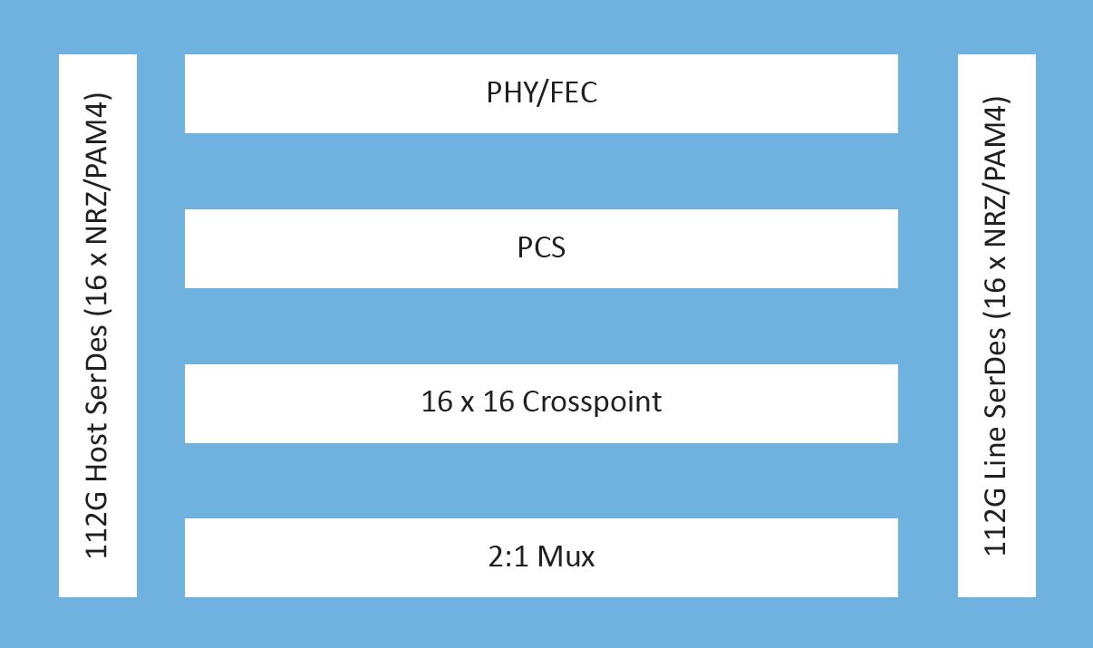
Microchip Technology’s latest physical layer (PHY) chip has been developed for next-generation line cards.
The PM6200 Meta-DX2L (the ‘L’ is for light) 1.6-terabit chip is implemented using TSMC’s 6nm CMOS process. It is Microchip’s first PHY to use 112-gigabit PAM-4 (4-level pulse-amplitude modulation) serialiser/ deserialisers (serdes) interfaces.
Microchip’s existing 16nm CMOS Meta-DX1 PHY devices are rated at 1.2 terabits and use 56-gigabit PAM-4 serdes.
System vendors developing line cards that double the capacity of their switch, router or transport systems are being challenged by space and power constraints, says Microchip. To this aim, the company has streamlined the Meta-DX2L to create a compact, lower-power chip.
“One of the things we have focussed on is the overall footprint of our [IC] design to ensure that people can realise their cards as they go to the 112-gigabit PAM-4 generation,” says Stephen Docking, manager, product marketing, communications business unit, at Microchip.
The company says the resulting package measures 23x30mm and reduces the power per port by 35 per cent compared to the Meta-DX1.
IC architecture
The Meta-DX1 family of 1.2-terabit physical layer (PHY) Ethernet chips effectively comprise three 400-gigabit cores and support the OIF’s Flexible Ethernet (FlexE) protocol and MACsec encryption.
The Meta-DX1 devices, launched in 2019, support the Precision Time Protocol (PTP) used to synchronise clocks across a network with high accuracy that is a requirement for 5G.
The new Meta-DX2L is a single chip although Microchip hints that other family devices will follow.
The Meta-DX2L can be viewed as comprising two 800-gigabit cores. The chip does away with FlexE and the PTP protocol but includes retiming and gearbox modes. The gearbox is used to translate between 28, 56 and 112-gigabit rates.
“We still see customers working on FlexE designs, so the lack of it [with the Meta-DX2L] is not due to limited market demand but how we chose to optimise the chip,” says Docking.
The same applies to PTP. The Meta-DX1 performs time stamping that meets 5G’s Class C and Class D front-haul clocking requirements. “The difference with the Meta-DX2L is that it is not doing time stamping,” says Docking. But it can work with devices doing the time stamping.
“In a 5G system, if you add a PHY, you need to do it in such a way that it doesn’t add any uncertainty in the overall latency of the system,” says Docking. ”So we have focussed on the device have a constant latency.” This means the Meta-DX2L can be used in systems meeting Class C or Class D clocking requirements.
The chip also features a 16×16 crosspoint switch that allows customers to use different types of optical modules and interface them to a line card’s ASIC or digital signal processor (DSP).
The Meta-DX2L’s two cores are flexible and support rates from 1 to 800 Gigabit Ethernet, says Docking.
As well as Ethernet rates, the device supports proprietary rates common with artificial intelligence (AI) and machine learning.
For AI, an array of graphic processor units (GPUs) talk to each other on the same line card. “But to scale the system, you have to have multiple line cards talk to each other,” says Docking. “Different companies that design GPUs have chosen their own protocols to optimise their communications.”
Such links are not aligned with the Ethernet rates but the Meta-DX2L supports these proprietary rates.
Microchip says the Meta-DX2L will sample this quarter.
1.6 terabits, system resilience and design challenges
The PHY’s 1.6-terabit capacity was chosen based on customers’ requirements.
“If you look at the number of ports people want to support, it is often an even multiple of 800-gigabit ports,” says Docking.
The Meta-DX2L, like its predecessor PHY family, has a hitless 2:1 multiplexer. The multiplexer function is suited for centralised switch platforms where the system intelligence resides on a central card while the connecting line cards are relatively simple, typically comprising PHYs and optical modules.
In such systems, due to the central role of the platform’s switch card, a spare card is included. Should the primary card fail, the backup card kicks in, whereby all the switch’s line cards connect to the backup. The 2:1 multiplexer in the PHY means each line card is interfaced to both switch cards: the primary one and backup.

For line cards that will have 32 or 36 QSFP-DD800 pluggable modules, space is a huge challenge, says Docking: “So having a compact PHY is important.”
“The physical form factor has always been a challenge and then density plays into it and thermal issues,” says Kevin So, associate director, product line management and marketing, communications business unit, at Microchip. “And when you overlay the complexity of the transition from 56 to 112 gigabits, that makes it extremely challenging for board designers.”
Applications
The 1.6-terabit PHY is aimed at switching and routing platforms, compact data centre interconnect systems, optical transport and AI designs.
Which application takes off first depends on several developments. On one side of the PHY chip sits the optics and on the other the ASIC, whether a packet processor, switch chip, processor or DSP. “It’s the timing of those pieces that drive what applications you will see first,” says So.
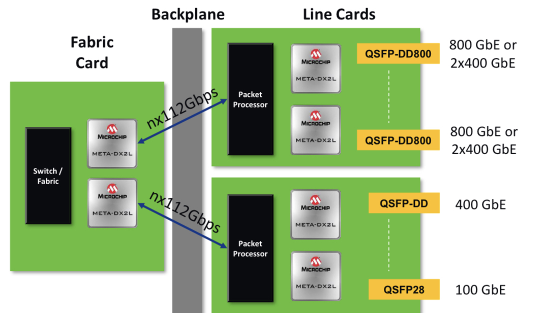
“Switching and packet processor chips are transitioning to 112-gigabit serdes and you are also starting to see QSFP-DD or OSFP optics with 112-gigabit serdes becoming available,” adds Docking. “So the ecosystem is starting for those types of systems.”
The device is also being aimed at routers for 5G backhaul applications. Here data rates are in the 10- to the 100-gigabit range. “But you are already starting to hear about 400-gigabit rates for some of these access backhaul routers,” says So.
And with 400 Gigabit Ethernet being introduced on access pizza-box routers for 5G this year, in two years, when Microchip’s customers release their hardware, there will likely be denser versions, says So.
“And by then we’ll be talking about a DX3, who knows?” quips So.

Deutsche Telekom’s edge for cloud gaming

Deutsche Telekom believes its network gives it an edge in the emerging game-streaming market.
The operator is trialling a cloud-based service similar to the likes of Google and Microsoft.
The operator already offers IP TV and music as part of its entertainment offerings and will decide if gaming will be the third component. The operator will launch its MagentaGaming cloud-based service in 2020.
“Since 2017, the biggest market in entertainment is gaming,” says Dominik Lauf, project lead, MagentaGaming at Deutsche Telekom.
Market research firms vary in their estimates but the global video gaming market was of the order of $138 billion in 2018 while the theatrics and home entertainment market totalled just under $100 billion for the same period.
Cloud Gaming
In Germany, half the population play video games with half of those being young adults. The gaming market represents a valuable opportunity to ‘renew the brand’ with a younger audience.
Until now, a user’s gaming experience has been determined by the video-processing capabilities of their gaming console or PC graphics card.
The advent of cloud-based gaming changes all that. A user not only can access the latest game titles via the cloud, they no longer need to own state-of-the-art equipment for the ultimate gaming experience. Instead, video processing for gaming is performed in the cloud. All that the user needs is a display. Any display; a smartphone, tablet, PC or TV.
Lauf says hardcore gamers typically spend over €1,000 each year on equipment, while some 45 per cent of all gamers can’t play the latest games at the highest display quality because their hardware is not up to the task. “[With cloud gaming,] the entry barrier of hardware no longer exists for customers,” says Lauf.
However, for game-streaming to work, the onus is on the service provider to deploy hardware – dedicated servers hosting high-end graphics processing units (GPUs) – and ensure that the game-streaming traffic is delivered efficiently over the network.
Deutsche Telekom points out that while buffering is used for video or music streaming services, this isn’t an option with gaming given its real-time nature.
“Latency and bandwidth play a pivotal role within gaming,” says Lauf. “Connectivity counts here.”
Networking demands
Deutsche Telekom’s game-streaming service requires a 50 megabit-per-second (Mbps) broadband connection.
Gaming traffic requires between 30-40Mbps of capacity to ensure full graphics quality. This is over four times the bandwidth required for a video stream. “We can lower the bandwidth required [for gaming] but you will notice it when using a bigger screen,” says Lauf.
The operator is testing the bandwidth requirements its mobile network must deliver to ensure the required gaming quality.
“With 5G, the bandwidth is more or less there, but bandwidth is not the only point, maybe the more important topic is latency,” says Lauf. The operator has recently launched 5G in five cities in Germany.
An end-to-end latency of 50-80ms ensures a smooth gaming experience. A latency of 100ms decreases an individual’s game-play while a latency of 120ms noticeably impacts responsiveness.
Deutsche Telekom’s fixed network delivers a sub-50ms latency. However, the home environment must also be factored in: the home’s wireless network and signal coverage, as well as other electronic devices in the home, all can influence gaming performance.
And it is not just latency that counts but jitter: the volatility of the latency. “The average may be below 50ms but if there are peaks at 100ms, it will impact your gameplay,” says Lauf.
Moreover, the latency and jitter performance should ideally be consistent across the network; otherwise, it can give an unfair advantage to select users in multi-player games.
5G and edge computing
The MegentaGaming trial is also being used to test how 5G and edge computing – where the servers and GPUs are hosted at the network edge – can deliver a sufficiently low jitter.
5G will provide more bandwidth than the operator’s existing LTE mobile network. This will not only benefit individual game players but also the size of group-gaming plays. At present, hundreds can play each other in a game but this number will grow, says Lauf.
5G will also enable new features, such as network slicing, that will benefit low jitter, says Lauf.
“‘Edge’ is a fuzzy term,” says Lauf. “But we will build our servers in a decentralised way to ensure latency does not affect gamers.”
MobiledgeX, a Deutsche Telekom spin-out that focusses on cloud infrastructure, operates four data centres in Germany and is also testing GPUs. However, for the test phase of MagentaGaming, Deutsche Telekom is deploying its servers and GPUs at the network edge
Lauf says the complete architecture must be designed with latency in mind: “There are a lot of components that can increase latency.” Not only the network but the GPU run times and the storage run times.
Deploying servers and GPUs at the network edge requires investment. And given that cloud gaming is still being trialled, it is too early to assess gaming’s business success.
So how does Deutsche Telekom justify investing in edge infrastructure and will the edge be used for other tasks as well as gaming?
“This is also a focus of our trial, to see when are the server peak times in terms of usage,” says Lauf. “There are capabilities for other use cases on the same GPUs.”
The operator is considering using the GPUs for artificial intelligence tasks.
Cloud-gaming competition
Microsoft and Google are also pursuing gaming-streaming services.
Microsoft is about to launch a preview of xCloud – its Xbox cloud-based service – and has been accepting registrations in certain countries.
Microsoft, too, recognises the importance of network latency and is working with operators such as SK Telecom in South Korea and Vodafone UK. It has also signed an agreement with T-Mobile, the US operator arm of Deutsche Telekom.
Meanwhile, Google is preparing its Stadia service which will launch next month.
Lauf believes Deutsche Telekom has an edge despite such hyperscaler competition.
“We are sure that with our high-quality network – our edge and 5G latency capabilities, and our last mile to our customer – we have an advantage compared to the hyperscalers given how latency and bandwidth count,” he says.
Gaming content also matters and the operator says it is in discussions with gaming developers that welcome the fact that there are alternatives to the hyperscalers’ platforms.
“We are quite sure we can play a role,” concludes Lauf. “Even if we are not on the same global level of a Google, we will have a right to play in this business.”
Game on!