
Lumentum's optical circuit switch for AI data centres
Part 3: Data Centre Switching
The resurgence of optical circuit switches for use in data centres is gaining momentum, driven by artificial intelligence (AI) workloads that require scalable connectivity.
Lumentum is one of several companies that showcased an optical circuit switch at the OFC event in San Francisco in March. Lumentum’s R300 switch connects optically the 300 input ports to any of the 300 output ports. The optical circuit switch uses micro-electro-mechanical systems (MEMS), tiny mirrors that move electrostatically, to direct light from an input port to one of the 300 output ports.
The R300 addresses the network needs of AI data centres, helping link large numbers of AI accelerator chips such as graphics processor units (GPUs).
“We’ve been talking to all the hyperscalers in North America and China,” says Peter Roorda, general manager of the switching business unit at Lumentum. “The interest is pretty broad for the applications of interconnecting GPUs and AI clusters; that’s the exciting one.”
Optical circuit switches
In a large-scale data centre, two or three tiers of electrical switch platforms link the many servers’ processors. The number of tiers needed depends on the overall processor count. The same applies to the back-end network used for AI workloads. These tiers of electrical switches are arranged in what is referred to as a Clos or “Fat Tree” architecture.
Google presented a paper in 2022 revealing that it had been using an internally developed MEMS-based optical circuit switch for several years. Google used its optical circuit switches to replace all the top-tier ‘spine’ layer electrical switches across its data centres, resulting in significant cost and power savings.
Google subsequently revealed a second use for its switches to directly connect between racks of its tensor processor unit (TPU) accelerator chips. Google can move workloads across thousands of TPUs in a cluster, efficiently using its hardware and bypassing a rack when a fault arises.
Google’s revelation rejuvenated interest in optical switch technology, and at OFC, Lumentum showed its first R300 optical switch product in operation.
Unlike packet switches, which use silicon to process data at the packet level, an optical circuit switch sets up a fixed, point-to-point optical connection, akin to a telephone switchboard, for the duration of a session.
The optical switch is ideal for scenarios where large, sustained data flows are required, such as in AI training clusters.

Merits
The optical circuit switch’s benefits include cost and power savings and improved latency. Optical-based switch ports are data-rate independent. They can support 400 gigabit, 800 gigabit, and soon 1.6-terabit links without requiring an upgrade.
“Now, it’s not apples to apples; the optical circuit switch is not a packet switch,” says Roorda. “It’s just a dumb circuit switch, so there must be control plane software to manage it.” However, the cost, power, space savings, and port transparency incentives suffice for the hyperscalers to invest in the technology.
The MEMS-based R300
Lumentum has a 20-year history using MEMS. It first used the technology in its wavelength-selective switches used in telecom networks before the company adopted liquid crystal on silicon (LCOS) technology.
“We have 150,000 MEMS-based wavelength selective switches in the field,” says Roorda. “This gives us a lot of confidence about their reliability.”
MEMS-based switches are renowned for their manufacturing complexity, and Lumentum has experience in MEMS.
“This is a key claim as users are worried about the mechanical aspect of MEMS’ reliability,” says Michael Frankel, an analyst at LightCounting Market Research, which published an April report covering Ethernet, Infiniband and optical switches in cloud data centres. “Having a reliable volume manufacturer is critical.”
In its system implementation, Google revealed that it uses bi-directional transceivers in conjunction with the OCS.
“Using bi-directional ports is clever because you get to double the ports out of your optical circuit switch for the same money, “says Mike DeMerchant, Lumentum’s senior director of product line management, optical circuit switch. “But then you need customised, non-standard transceivers.”
A bi-directional design complicates the control plane management software because bi-directional transponders effectively create two sets of connections. “The two sets of transceivers can only talk in a limited fashion between each other, so you have to manage that additional control plane complexity,” says DeMerchant.
Lumentum enters the market with a 300×300 radix switch. Some customers have asked about a 1,000×1,000 port switch. From a connectivity perspective, bigger is better, says Roorda. “But bigger is also harder; if there is a problem with that switch, the consequences of a failure—the blast radius—are larger too,” he says.

Lumentum says there are requests for smaller optical circuit switches and expects to offer a portfolio of different-sized products in the next two years.
The R300 switch is cited as having a 3dB insertion loss, but Roorda says the typical performance is close to 1.5dB at the start of life. “And 3dB is good enough for using a standard off-the-shelf -FR4 or a -DR4 or -DR8 optical module [with the switch],” says Roorda.
A 400G QSFP-DD FR4 module uses four wavelengths on a single-mode fibre and has a reach of 2km, whereas a DR4 or DR8 uses a single wavelength on each fibre and has 4 or 8 single-mode fibre outputs, respectively, with a reach of 500m.
An FR4 interface is ideal with an optical circuit switch since multiple wavelengths are on a single fibre and can be routed through one port. However, many operators use DR4 and DR8 interfaces and are exploring using such transceivers.
“More ports would be consumed, diluting the cost-benefit, but the power savings would still be significant,” says Roorda.Additionally, in some applications, individually routing and recombining the separate ‘rails’ of DR4 or DR8 offer greater networking granularity. Here, the optical circuit switch still provides value, he says.
One issue with an optical circuit switch compared to an electrical-based one is that the optics go through both optical ports before reaching the destination transceiver, adding an extra 3dB loss. By contrast, for an electrical switch, the signal is regenerated optically by the pluggable transceiver at the output port.
LightCounting’s Frankel also highlights the switch’s loss numbers. “Lumentum’s claim of a low loss – under 2dB – and a low back reflection (some 60dB) are potential differentiators,” he says. “It is also a broadband design – capable of operating across the O-, C- and L-bands: O-band for data centre and C+L for telecom.”
Software and Hyperscaler Control
Lumentum is controlling the switch using the open-source SONiC [Software for Open Networking in the Cloud] network operating system (NOS), based on Linux. The hyperscalers will add the higher-level control plane management software using their proprietary software.
“It’s the basic control features for the optics, so we’re not looking to get into the higher control plane,” says DeMerchant.
Challenges and Scalability
Designing a 300×300 optical circuit switch is complicated. “It’s a lot of mirrors,” says Roorda. “You’ve got to align them, so it is a complicated, free-space, optical design.”
Reliability and scalable manufacturing are hurdles. “The ability to build these things at scale is the big challenge,” says Roorda. Lumentum argues that its stable MEMS design results in a reliable, simpler, and less costly switch.Lumentum envisions data centres evolving to use a hybrid switching architecture, blending optical circuit switches with Ethernet switches.
Roorda compares it to how telecom networks transitioned to using reconfigurable optical add-drop multiplexers (ROADMs).”It’ll be hybridised with packet switches because you need to sort the packets sometimes,” says Roorda.
Future developments may include multi-wavelength switching and telecom applications for optical circuit switches. “For sure, it is something that people are talking about,” he adds.
Lumentum says its R300 will be generally available in the second half of this year.

Has the era of co-packaged optics finally arrived?
Ayar Labs’ CEO, Mark Wade
Mark Wade, the recently appointed CEO of Ayar Labs, says his new role feels strangely familiar. Wade finds himself revisiting tasks he performed in the early days of the start-up that he helped co-found.
“In the first two years, I would do external-facing stuff during the day and then start working on our chips from 5 PM to midnight,” says Wade, who until last year was the company’s chief technology officer (CTO).
More practically, says Wade, he has spent much of the first months since becoming CEO living out of a suitcase and meeting with customers, investors, and shareholders.
History
Ayar Labs is bringing its technology to market to add high-bandwidth optical input-output (I/O) to large ASICs.
The technology was first revealed in a 2015 paper published in the science journal, Nature. In it, the optical circuitry needed for the interfaces was implemented using a standard CMOS process.
Vladimir Stojanovic, then an associate professor of electrical engineering and computer science at the University of California, Berkeley, described how, for the first time, a microprocessor could communicate with the external world using something other than electronics.
Stojanovic has left his role as a professor at the University of California, Berkeley, to become Ayar Labs’ CTO, following Wade’s appointment as CEO.

Focus
“A few years ago, we made this pitch that machine-learning clusters would be the biggest opportunity in the data centre,” says Wade. “And for efficient clusters, you need optical I/O.” Now, connectivity in artificial intelligence (AI) systems is a vast and growing problem. “The need is there, and our product is timed well,” says Wade.
Ayar Labs has spent the last year focusing on manufacturing and established low-volume production lines. The company manufactured approximately 10,000 optical chiplets in 2023 and expects similar volumes this year. The company also offers an external laser source SuperNova product that provides the light source needed for its optical chiplet.
 Ayar Labs’ optical input-output (I/O) roadmap showing the change in electrical I/O interface evolving from Intel’s AIB to the UCIe standard, the move to faster data rates and, on the optical side, more wavelengths and the growing total I/O, per chiplet and packaged system. Source: Ayar Labs.
The products are being delivered to early adopter customers while Ayar Labs establishes the supply chain, product qualification, and packaging needed for volume manufacturing.
Wade says that some of its optical chiplets are being used for other non-AI segments. Ayar Labs has demonstrated its optical I/O being used with FPGAs for electronics systems for military applications. But the primary demand is for AI systems connectivity, whether compute to compute, compute to memory, compute to storage, and compute to a memory-semantic switch.
“A memory-semantic switch allows the scaling of a compute fabric whereby a bunch of devices need to talk to each other’s memory,” says Wade.
Wade cites Nvidia’s NVSwitch as one example: the first layer switch chip at the rack level that supports many GPUs in a non-blocking compute fabric. Another example of a memory-semantic switch is the open standard Compute Express Link (CXL).
The need for co-packaged optics
At the Optica Executive Forum event held alongside the recent OFC show, several speakers questioned the need for I/O based on optical chiplets, also called co-packaged optics.
Google’s Hong Liu, a Distinguished Engineer at Google Technical Infrastructure, described co-packaged optics as an ’N+2 years’ technology, perpetually coming in two years’ time, (N being the current year).
Ashkan Seyedi of Nvidia stressed that copper continues to be the dominant interconnect for AI because it beats optics in such metrics as bandwidth density, power, and cost. Existing data centre optical networking technology cannot simply be repackaged as optical compute I/O, as it does not beat copper. Seyedi also shared a table that showed how much more expensive optical was in terms of dollar per gigabit/second ($/ Gbps).
Wade starts to address these points by pointing out that nobody is making money at the application layer of AI. Partly, this is because the underlying hardware infrastructure for AI is so costly.
“It [the infrastructure] doesn’t have the [networking] throughput or power efficiency to create the headroom for an application to be profitable,” says Wade.
The accelerator chips from the likes of Nvidia and Google are highly efficient in executing the mathematics needed for AI. But it is still early days when it comes to the architectures of AI systems, and more efficient hardware architectures will inevitably follow.
AI workloads also continue to grow at a remarkable rate. They are already so large that they must be spread across systems using ever more accelerator chips. With the parallel processing used to execute the workloads, data has to be shared periodically between all the accelerators using an ’all-to-all’ command.
“With large models, machines are 50 per cent efficient, and they can get down to 30 per cent or even 20 per cent,” says Wade. This means expensive hardware is idle for more than half the time. And the issue will only worsen with growing model size. According to Wade, using optical I/O promises the proper bandwidth density – more terabits-per-second per mm, power efficiency, and latency.
“These products need to get proven and qualified for volume productions,” he adds. “They are not going to get into massive scale systems until they are qualified for huge scale production.”
Wade describes what is happening now as a land grab. Demand for AI accelerators is stripping supply, and the question is still being figured out as to how the economics of the systems can be improved.
“It is not about making the hardware cheaper, just how to ensure the system is more efficiently utilised,” says Wade. “This is a big capital asset; the aim is to have enough AI workload throughput so end-applications have a viable cost.”
This will be the focus as the market hits its stride in the coming two to three years. “It is unacceptable that a $100 million system is spending up to 80 per cent of its time doing nothing,” says Wade.
Wade also addresses the comments made the day at the Optica Executive Forum. “The place where [architectural] decisions are getting discussed and made are with the system-on-chip architects,” he says. “It’s they that decide, not [those at] a fibre-optics conference.”
He also questions the assumption that Google and Nvidia will shun using co-packaged optics.
Market opportunity
Wade does a simple back-of-an-envelope calculation to size the likely overall market opportunity by the early 2030s for co-packaged optics.
In the coming years, there will be 1,000 optical chiplets per server, 1,000 servers per data centre, while 1,000 new data centres using AI clusters will be built. That’s a billion devices in total. Even if the total addressable opportunity is several hundred million optical chiplets, that is still a massive opportunity by 2032, he says.
Wade expects Ayar Labs to ship 100,000 plus chiplets in the 2025-26 timeframe, with volumes ramping to the millions in the two years after that.
“That is the ramp we are aiming for,” he says. “Using optical I/O to build a balanced composable system architecture.” If co-packaged optics does emerge in such volumes, it will disrupt the optical component business and the mainstream technologies used today.
“Let me finish with this,” says Wade. “If we are still having this conversation in two years’ time, then we have failed.”

Drut tackles disaggregation at a data centre scale
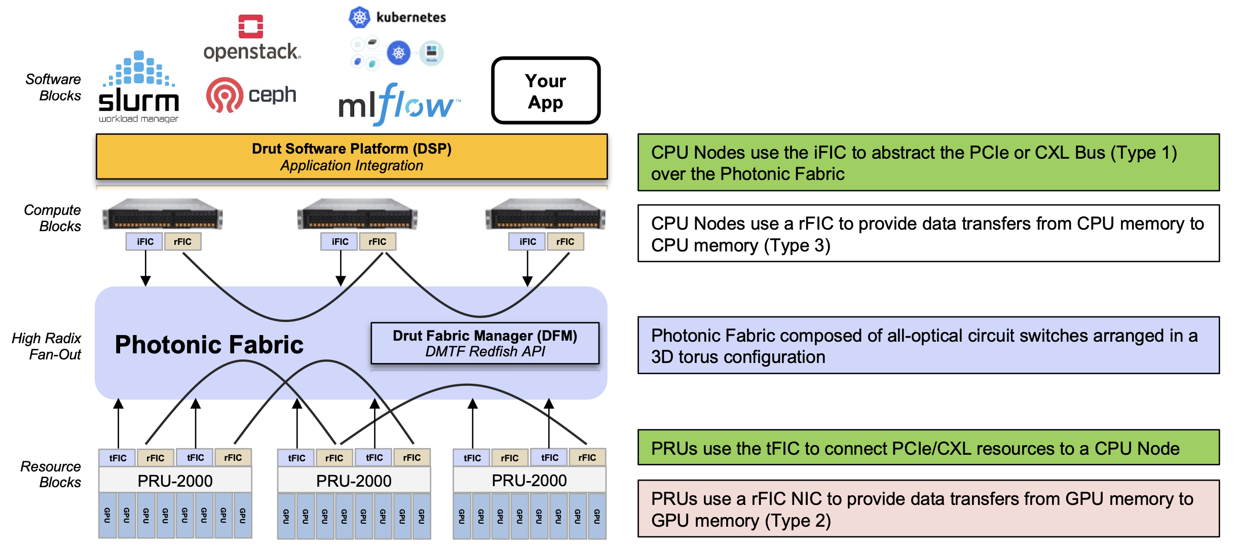
- Drut’s DynamicXcelerator supports up to 4,096 accelerators using optical switching and co-packaged optics. Four such clusters enable the scaling to reach 16,384 accelerators.
- The system costs less and is cheaper to run, has lower latency, and better uses the processors and memory.
- The system is an open design supporting CPUs and GPUs from different vendors.
- DynamicXcelerator will ship in the second half of 2024.
Drut Technologies has detailed a system that links up to 4,096 accelerator chips. And further scaling, to 16,384 GPUs, is possible by combining four such systems in ‘availability zones’.
The US start-up previously detailed how its design can disaggregate servers, matching the processors, accelerators, and memory to the computing task at hand. Unveiled last year, the product comprises management software, an optical switch, and an interface card that implements the PCI Express (PCIe) protocol over optics.
The product disaggregates the servers but leaves intact the tiered Ethernet switches used for networking servers across a data centre.
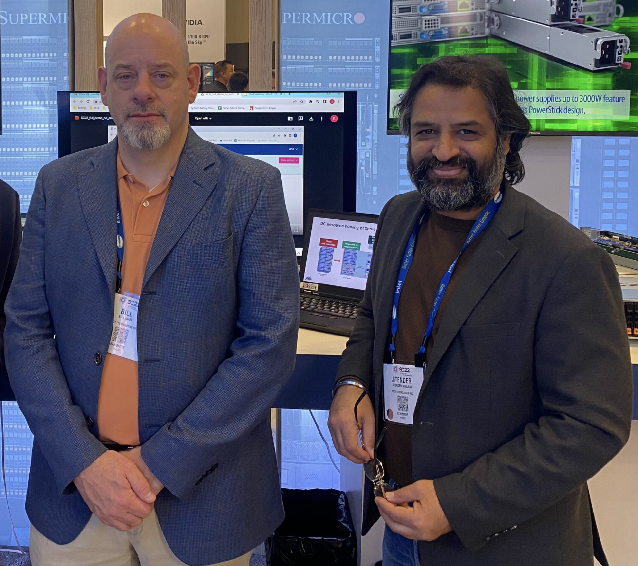
Now the system start-up is expanding its portfolio with a product that replaces the Ethernet switches with optical ones. “You can compose [compute] nodes and drive them using our software,” says Bill Koss, CEO of Drut.
Only Google has demonstrated the know-how to make such a large-scale flexible computing architecture using optical switching.
Company background
Drut was founded in 2018 and has raised several funding rounds since 2021.
Jitender Miglani, founder and president of Drut, previously worked at MEMS-based optical switch maker, Calient Technologies.
Drut’s goal was to build on its optical switching expertise and add the components needed to make a flexible, disaggregated computing architecture. “The aim was building the ecosystem around optical switches,” says Miglani.
The company spent its first two years porting the PCIe protocol onto an FPGA for a prototype interface card. Drut showcased its prototype product alongside a third-party optical switch as part of a SuperMicro server rack at the Supercomputing show in late 2022.
Drut has spent 2023 developing its next-generation architecture to support clusters of up to 4,096 endpoints. These can be accelerators like graphics processing units (GPUs), FPGAs, data processing units (DPUs), or storage using the NVM Express (nonvolatile memory express).
The architecture, dubbed DynamicXcelerator, supports PCIe over optics to link processors (CPUs and GPUs) and RDMA (Remote Direct Memory Access) over optics for data communications between the GPUs and between the CPUs.
The result is the DynamicXcelerator system, a large-scale reconfigurable computing for intensive AI model training and high-performance computing workloads.
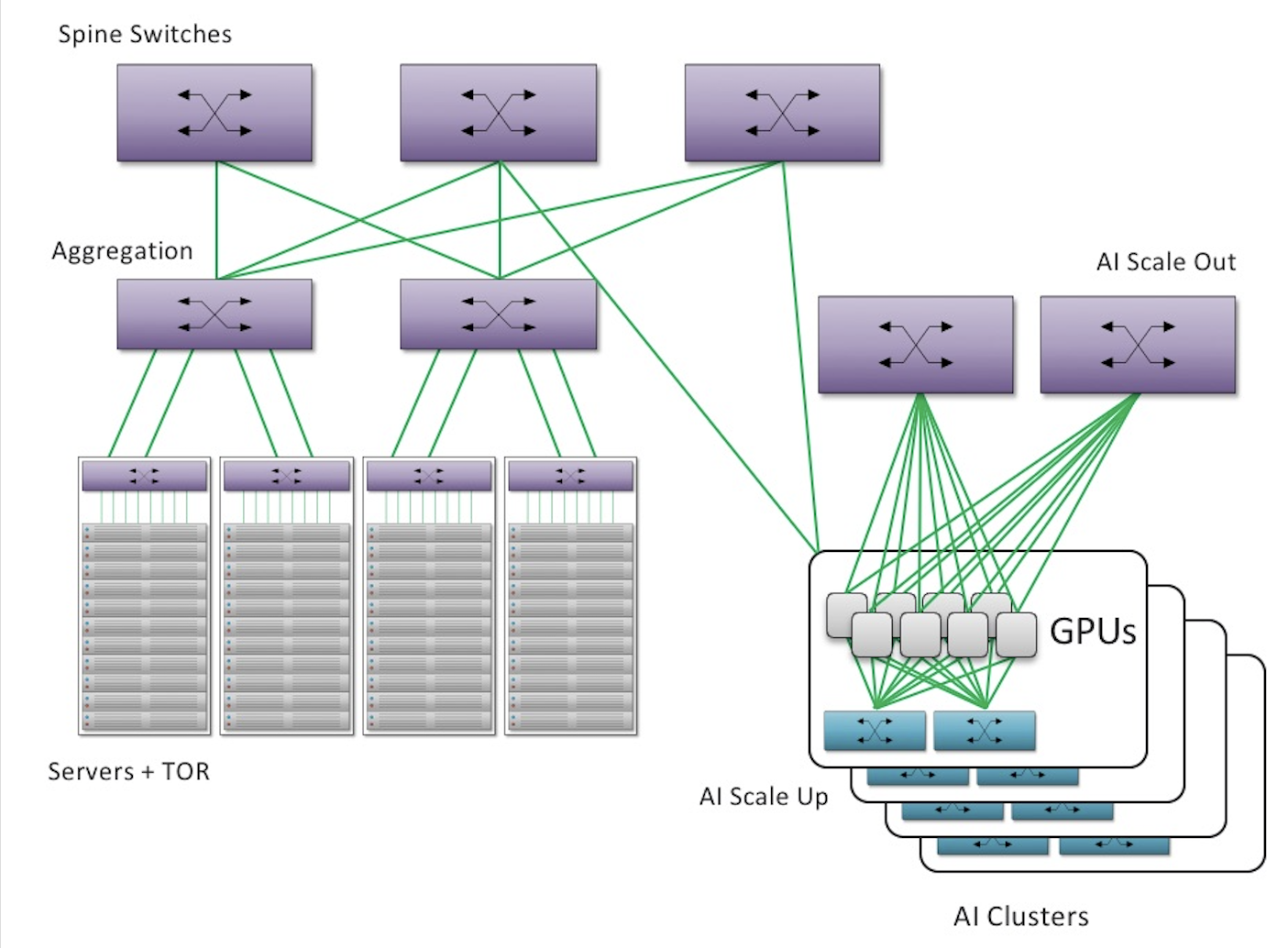
DynamicXcelerator
The core of the DynamicXcelerator architecture is a photonic fabric based on optical switches. This explains why Drut uses PCIe and RDMA protocols over optics.
Optical switches brings size and flexibility and by relaying optical signals, their ports are data-rate independent.
Another benefit of optical switching is power savings. Drut says an optical switch consumes 150W whereas an equivalent-sized packet switch consumes 1,700W. On average, an Infiniband or Ethernet packet switch draws 750W when used with passive cables. Using active cables, the switch’s maximum power rises to 1,700W. “[In contrast], a 32-64-128-144 port all-optical switch draws 65-150W,” says Koss.
Drut also uses two hardware platforms. One is the PCIe Resource Unit, dubbed the PRU-2000, which hosts eight accelerator chips such as GPUs. Unlike Nvidia’s DGX platform, which uses Nvidia GPUs such as the Hopper, or Google, which uses its TPU5 tensor processor unit (TPU), Drut’s PRU-2000 is an open architecture and can use GPUs from Nvidia, AMD, Intel, and others. The second class of platform is the compute node or server, which hosts the CPUs.
DynamicXcelerator’s third principal component are the FIC 2500 interface cards.
The iFIC 2500 card is similar to Drut’s current product’s iFIC 1000, which features an FPGA and four QSFP28s. However, the iFIC 2500 supports the PCIe 5.0 generation bus and the Compute Express Link (CXL) protocols. The two other FIC cards are the tFIC 2500 and rFIC 2500.
“The iFIC and tFIC are the same card, but different software images,” says Koss. “The iFIC fits into a compute node or server while the tFIC fits into our Photonic Resource Unit (PRU) unit, which holds GPUs, FPGAs, DPUs, NVMe, and the like.”
The rFIC provides RDMA over photonics for GPU-to-GPU memory sharing. The rFIC card for CPU-to-CPU memory transfers is due later in 2024.
Miglani explains that PCIe is used to connect the GPUs and CPUs, but for GPU-to-GPU communication, RDMA is used since even PCIe over photonics has limitations.
Certain applications will use hundreds and even thousands of accelerators, so a PCIe lane count is one limitation, distance is another; a 5ns delay is added for each metre of fibre. “There is a window where the PCIe specification starts to fall off,” says Miglani.
The final component is DynamicXcelerator’s software. There are two software systems: the Drut fabric manager (DFM), which controls the system’s hardware configuration and traffic flows, and the Drut software platform (DSP) that interfaces applications onto the architecture.
Co-packaged optics
Drut knew it would need to upgrade the iFIC 1000 card. DynamicXcelerator uses PCIe 5.0, each lane being 32 gigabit-per-second (Gbps). Since 16 lanes are used, that equates to 512 gigabits of bandwidth.
“That’s a lot of bandwidth, way more that you can crank out with four 100-gigabit pluggables,” says Koss, who revealed co-packaged optics will replace pluggable modules for the iFIC 2500 and tFIC 2500 cards.
The card for the iFIC and tFIC will use two co-packaged optical engines, each 8×100 gigabits. The total bandwidth of 1.6 terabits – 16×100-gigabit channels – is a fourfold increase over the iFIC 1000.
System workings
The system’s networking can be viewed as a combination of circuit switching and packet switching.
The photonic fabric, implemented as a 3D torus (see diagram), supports circuit switching. Using a 3D torus, three hops at most are needed to link any two of the system’s endpoints.
One characteristic of machine learning training, such as large language models, is that traffic patterns are predictable. This suits an architecture that can set the resources and the connectivity for a task’s duration.
Packet switching is not performed using Infiniband. Nor is a traditional spine-leaf Ethernet switch architecture used. The DynamicXcelerator does uses Ethernet but in the form of a small, distributed switching layer supported in each interface card’s FPGA.
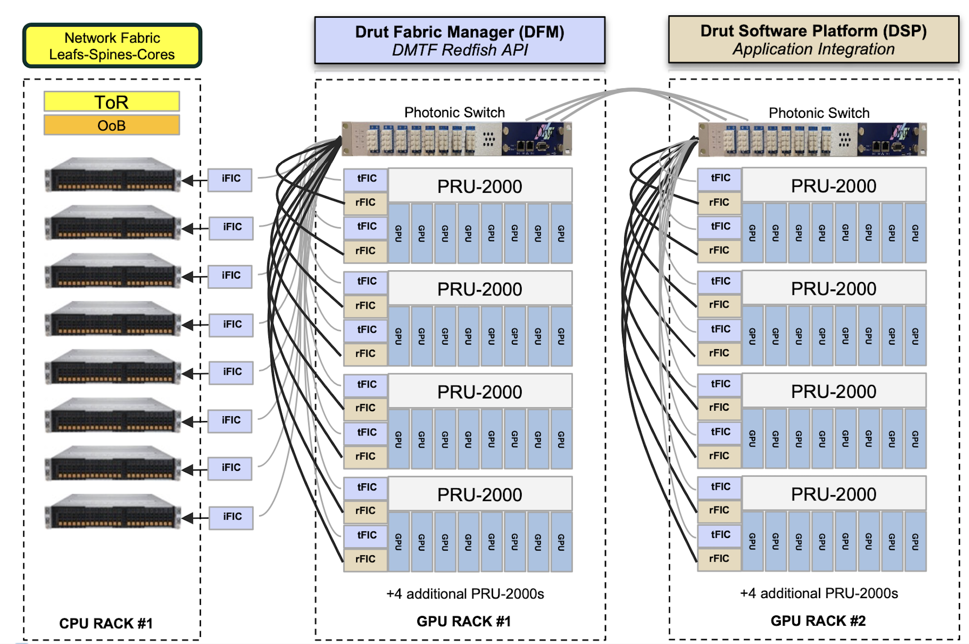
The smallest-sized DynamicXcelerator would use two racks of stacked PRU-2000s (see diagram). Further racks would be added to expand the system.
“The idea is that you can take a very large construct of things and create virtual PODs,” says Koss. “All of a sudden, you have flexible and fluid resources.”
Koss says a system can scale to 16,384 units by combining four clusters, each of 4,096 accelerators. “Each one can be designated as an ‘availability zone’, with users able to call resources in the different zones,” he says.
Customers might use such a configuration to segment users, run different AI models, or for security reasons. “It [a 16,384 unit system] would be huge and most likely something that only a service provider would do or maybe a government agency,” says Koss.
Capital and operation savings
Drut claims the architecture costs 30 per cent less than conventional systems, while operational cost-savings are 40 per cent.
The numbers need explaining, says Koss, given the many factors and choices possible.
The bill of materials of a 16, 32, 64 or 128-GPU design has a 10-30 per cent saving solely from the interconnect.
“The bigger the fabric, the better we scale in price as solutions using tiered leaf-spine-core packet switches involving Ethernet-Infiniband-PCIe are all built around the serdes of the switch chip in the box,” says Koss. “We have a direct-connect fabric with a very high radix, which allows us to build the fabric without stacked tiers like legacy point-to-point networks.”
There are also the power savings, as mentioned. Less power means less heat and hence less cooling.
“We can also change the physical wires in the network,” says Koss, something that can’t be done with leaf-spine-core networks, unless data centre staff change the cabling.
“By grouping resources around a workload, utilisation and performance are much better,” says Koss. “Apps run faster, infrastructure is grouped around workloads, giving users the power to do more with less.”
The system’s evolution is another consideration. A user can upgrade resources because of server disaggregation and the ability to add and remove resources from active machines.
“Imagine that you bought the DynamicXcelerator in 2024. Maybe it was a small sized, four-to-six rack system of GPUs, NVMe, etc,” says Koss. If, in mid-2026, Nvidia releases a new GPU, the user can take several PRU-2000s offline and replace the existing GPUs with the new ones.
“Also if you are an Nvidia shop but want to use the new Mi300 from AMD, no problem,” says Koss. “You can mix GPU vendors with the DynamicXcelerator.” This is different from today’s experience, where what is built is wasteful, expensive, complex, and certainly not climate-conscious, says Koss.
Plans for 2024
Drut has 31 employees, 27 of which are engineers. “We are going on a hiring binge and likely will at least double the company in 2024,” says Koss. “We are hiring in engineering, sales, marketing, and operations.”
Proof-of-concept DynamicXcelerator hardware will be available in the first half of 2024, with general availability then following.

Broadcom's first Jericho3 takes on AI's networking challenge
Add Content
Broadcom’s Jericho silicon has taken an exciting turn.
The Jericho devices are used for edge and core routers.
But the first chip of Broadcom’s next-generation Jericho is aimed at artificial intelligence (AI); another indicator, if one is needed, of AI’s predominance.
Dubbed the Jericho3-AI, the device networks AI accelerator chips that run massive machine-learning workloads.
AI supercomputers
AI workloads continue to grow at a remarkable rate.
The most common accelerator chip used to tackle such demanding computations is the graphics processor unit (GPU).
GPUs are expensive, so scaling them efficiently is critical, especially when AI workloads can take days to complete.
“For AI, the network is the bottleneck,” says Oozie Parizer, (pictured) senior director of product management, core switching group at Broadcom.
Squeezing more out of the network equates to shorter workload completion times.
“This is everything for the hyperscalers,” says Parizer. “How quickly can they finish the job.”
Broadcom shares a chart from Meta (below) showing how much of the run time for its four AI recommender workloads is spent on networking, moving the data between the GPUs.

In the worse case, networking accounts for three fifths (57 per cent) of the time during which the GPUs are idle, waiting for data.
Scaling
Parizer highlights two trends driving networking for AI supercomputers.
One is the GPU’s growing input-output (I/O), causing a doubling of the interface speed of network interface cards (NICs). The NIC links the GPU to the top-of-rack switch.
The NIC interface speeds have progressed from 100 to 200 to now 400 gigabits and soon 800 gigabits, with 1.6 terabits to follow.
The second trend is the amount of GPUs used for an AI cluster.
The largest cluster sizes have used 64 or 256 GPUs, limiting the networking needs. But now machine-learning tasks require clusters of 1,000 and 2,000 GPUs up to 16,000 and even 32,000.
Meta’s Research SuperCluster (RSC), one of the largest AI supercomputers, uses 16,000 Nvidia A100 GPUs: 2,000 Nvidia DGX A100 systems each with eight A100 GPUs. The RSC also uses 200-gigabit NICs.
“The number of GPUs participating in an all-to-all exchange [of data] is growing super fast,” says Parizer.
The Jericho3-AI is used in the top-of-rack switch that connects a rack’s GPUs to other racks in the cluster.
The Jericho3-AI enables clusters of up to 32,000 GPUs, each served with an 800-gigabit link.
An AI supercomputer can used all its GPUs to tackle one large training job or split the GPUs into pools running AI workloads concurrently.
Either way, the cluster’s network must be ‘flat’, with all the GPU-to-GPU communications having the same latency.
Because the GPUs exchange machine-learning training data in an all-to-all manner, only when the last GPU receives its data can the computation move onto the next stage.
“The primary benefit of Jericho3-AI versus traditional Ethernet is predictable tail latency,” says Bob Wheeler, principal analyst at Wheeler’s Network. “This metric is very important for AI training, as it determines job-completion time.”
Data spraying
“We realised in the last year that the premium traffic capabilities of the Jericho solution are a perfect fit for AI,” says Parizer.
The Jericho3-AI helps maximise GPU processing performance by using the full network capacity while traffic routing mechanisms help nip congestion in the bud.
The Jericho also adapts the network after a faulty link occurs. Such adaptation must avoid heavy packet loss otherwise the workload must be restarted, potentially losing days of work.
AI workloads use large packet streams known as ‘elephant’ flows. Such flows tie up their assigned networking path, causing congestion when another flow also needs that path.
“If traffic follows the concept of assigned paths, there is no way you get close to 100 per cent network efficiency,” says Parizer.
The Jericho3-AI, used in a top-of-rack switch, has a different approach.
Of the device’s 28.8 terabits of capacity, half connects the rack’s GPUs’ NICs and a half to the ‘fabric’ that links the rack’s GPUs to all the other cluster’s GPUs.
Broadcom uses the 14.4-terabit fabric link as one huge logical pipe over which traffic is evenly spread. Each destination Jericho3-AI top-of-rack switch then reassembles the ‘sprayed’ traffic.
“From the GPU’s perspective, it is unaware that we are spraying the data,” says Parizer.
Receiver-based flow control
Spraying may ensure full use of the network’s capacity, but congestion can still occur. The sprayed traffic may be spread across the fabric to all the spine switches, but for short periods, several GPUs may send data to the same GPU, known as incast (see diagram).

The Jericho copes with this many-to-one GPU traffic using receiver-based flow control.
Traffic does not leave the receiving Jericho chip just because it has arrived, says Parizer. Instead, the receiving Jericho tells the GPUs with traffic to send and schedules part of the traffic from each.
“Traffic ends up queueing nearer the sender GPUs, notifying each of them to send a little bit now, and now,” says Parizer, who stresses this many-to-one condition is temporary.
Ethernet flow control is used when Jericho chip senses that too much traffic is being sent.
“There is a temporary stop in data transmission to avoid packet loss in network congestion,” says Parizer. “And it is only that GPU that needs to slow down; it doesn’t impact any adjacent GPUs.”
Fault control
At Optica’s Executive Forum event, held alongside the OFC show in March, Google discussed using a 6,000 tensor processor unit (TPU) accelerator system to run large language models.
One Google concern is scaling such clusters while ensuring overall reliability and availability, given the frailty of large-scale accelerator clusters.
“With a huge network having thousands of GPUs, there is a lot of fibre,” says Parizer. “And because it is not negligible, faults happen.”
New paths must be calculated when an optical link goes down in a network arrangement that using flows and assigned paths with significant traffic loss likely.
“With a job that has been running for days, significant packet loss means you must do a job restart,” says Parizer.
Broadcom’s solution, not based on flows and assigned paths, uses load balancing to send data over one less path overall.
Using the Jericho2C+, Broadcom has shown fault detection and recovery in microseconds such that the packet loss is low and no job restart is needed.
The Jericho portfolio of devices
Broadcom’s existing Jericho2 architecture combines an enhanced packet-processing pipeline with a central modular database and a vast memory holding look-up tables.
Look-up tables are used to determine how the packet is treated: where to send it, wrapping it in another packet (tunnel encapsulation), extracting it (tunnel termination), and access control lists (ACLs).
Different stages in the pipeline can access the central modular database, and the store can be split flexibly without changing the packet-processing code.
Jericho2 was the first family device with a 4.8 terabit capacity and 8 gigabytes of high bandwidth memory (HBM) for deep buffering.
The Jericho 2C followed, targeting the edge and service router market. Here, streams have lower bandwidth – 1 and 10 gigabits typically – but need better support in the form of queues, counters and metering, used for controlling packets and flows.
Pariser says the disaggregated OpenBNG initiative supported by Deutsche Telekom uses the Jericho 2C.
Broadcom followed with a third Jericho2 family device, the Jericho 2C+, which combines the attributes of Jericho2 and Jericho2C.
Jericho2C+ has 14.4 terabits of capacity and 144 100-gigabit interfaces, of which 7.2-terabit is network interfacing bandwidth and 7.2-terabit for the fabric interface.
“The Jericho2C+ is a device that can target everything,” says Pariser.
Applications include data centre interconnect, edge and core network routing, and even tiered switching in the data centre.
Hardware design
The Jericho3-AI, made up of tens of billions of transistors in a 5nm CMOS process, is now sampling.
Broadcom says it designed the chip to be cost-competitive for AI.
For example, the packet processing pipeline is simpler than the one used for core and edge routing Jericho.
“This also translates to lower latency which is something hyperscalers also care about,” says Parizer.
The cost and power savings from optimisations will be relatively minor, says Wheeler.

Broadcom also highlights the electrical performance of the Jericho3-AI’s input-output serialiser-deserialiser (serdes) interfaces.
The serdes allows the Jericho3-AI to be used with 4m-reach copper cables linking the GPUs to the top-of-rack switch.
The serdes performance also enables linear-drive pluggables that dont have no digital signal processor (DSP) for retiming with the serdes driving the pluggable directly. Linear drive saves cost and power.
Broadcom’s Ram Valega, senior vice president and general manager of the core switching group, speaking at the Open Compute Project’s regional event held in Prague in April, said 32,000 GPU AI clusters cost around $1 billion, with 10 per cent being the network cost.

Valega showed Ethernet outperforms Infiniband by 10 per cent for a set of networking benchmarks (see diagram above).
“If I can make a $1 billion system ten per cent more efficient, the network pays for itself,” says Valega.
Wheeler says the comparison predates the recently announced NVLink Network, which will first appear in Nvidia’s DGX GH200 platform.
“It [NVLink Network] should deliver superior performance for training models that won’t fit on a single GPU, like large language models,” says Wheeler.

Enfabrica’s chip tackles AI supercomputing challenges
- Enfabrica’s accelerated compute fabric chip is designed to scale computing clusters comprising CPUs and specialist accelerator chips.
- The chip uses memory disaggregation and high-bandwidth networking for accelerator-based servers tackling artificial intelligence (AI) tasks.
For over a decade, cloud players have packed their data centres with x86-based CPU servers linked using tiers of Ethernet switches.
“The reason why Ethernet networking has been at the core of the infrastructure is that it is incredibly resilient,” says Rochan Sankar, CEO and co-founder of Enfabrica.
But the rise of AI and machine learning is causing the traditional architecture to change.
What is required is a mix of processors: CPUs and accelerators. Accelerators are specialist processors such as graphics processing units (GPUs), programmable logic (FPGAs), and custom ASICs developed by the hyperscalers.
It is the accelerator chips, not the CPUs, that do the bulk of the processing. Accelerators also require vast data, creating challenging input-output (I/O) and memory requirements.
At Optica’s Executive Forum event, held alongside the OFC show in March, Ryohei Urata, director and principal engineer at Google, mentioned how Google uses two computing pods – comprising 6,000 TPU accelerators – to run its large language models.
A key concern for Google is scaling such clusters while ensuring their reliability and availability. It is critical that the system is available when running a large language model, says Urata,
“As an engineer, when you’re putting stuff down, at least when you’re first start to put it together, you think, okay, this is going to work perfectly,” says Urata. “This is a perfect design, you don’t factor in failing gracefully, so that’s a key lesson.”
Google’s concern highlights that accelerator-based clusters lack the reliability of data centre server-Ethernet networks.
Accelerated compute fabric
Start-up Enfabrica has developed a chip, dubbed the accelerated compute fabric, to scale computing clusters.
“The focus of Enfabrica is on how networking and fabric technologies have to evolve in the age of AI-driven computing,” says Sankar.
AI models are growing between 8x to 275x annually, placing enormous demands on a data centre’s computing and memory resources.
“Two hundred and seventy-five times are of the order of what the large language models are increasing by, 8x is more other models including [machine] vision; recommender models are somewhere in between,” says Sankar.
Another AI hardware driver is growing end-user demand; ChatGPT gained 100 million users in the first months after its launch.
Meeting demand involves cascading more accelerators but the I/O bandwidth connected to the compute is lagging. Moreover, that gap is growing.
Sankar includes memory bandwidth as part of the I/O issue and segments I/O scaling into two: connecting CPUs, GPUs, accelerators and memory in the server, and the I/O scaling over the network.
A computing architecture for AI must accommodate greater CPUs and accelerators yet tackle the I/O bottleneck.
“To scale, it requires disaggregation; otherwise, it becomes unsustainable and expensive, or it can’t scale enough to meet processing demands,” says Sankar
“Memory disaggregation represents the last step in server disaggregation, following storage and networking,” says Bob Wheeler, principal analyst at Wheeler’s Network.
Memory expansion through disaggregation has become more urgent as GPUs access larger memories for AI training, particularly for large language modules like ChatGPT, says Wheeler.
Rethinking data connectivity
In the data centre, servers in a rack are linked using a top-of-rack switch. The top-of-rack switch also connects to the higher-capacity leaf-spine Ethernet switching layers to link servers across the data centre.
Enfabrica proposes that the higher capacity Ethernet switch leaf layer talks directly to its accelerated compute fabric chip, removing the top-of-rack switch.
In turn, the accelerated compute fabric uses memory mapping to connect CPUs, accelerators, disaggregated memory pools using CXL, and disaggregated storage (see diagram above).
The memory can be a CPU’s DDR DRAM, a GPU’s high-bandwidth memory (HBM), a disaggregated compute express link (CXL) memory array, or storage.
“It [the accelerated compute fabric] connects to them over standard memory-mapped interfaces such as PCI Express (PCIe) or CXL,” says Sankar.
The chip uses ‘copy engines’ to move data to and from any processing element’s native memory. And by performing memory transfers in parallel, the chip is doing what until now has required PCIe switches, network interface cards (NICs), and top-of-rack switches.
The accelerated compute fabric also has 800-gigabit network interfaces so that, overall, the chip has terabits of bandwidth to move data across the network.
“CXL provides a standard way to decouple memories from CPUs, enabling DRAM disaggregation,” says Wheeler. “Enfabrica’s copy engines connect the GPUs to the pool of CXL memory. The network side, using RDMA (remote direct memory access), enables scaling beyond the limits of CXL.”
Sankar stresses that the accelerated compute fabric is much more than an integration exercise using an advanced 5nm CMOS process.
“If you were to integrate eight NICs, four PCIe switches and a top-of-rack switch, it would not fit into a single die,” says Sankar.
As for software, Enfabrica has designed its solution to fit in with how GPUs, CPUs and memory move data.
Significance
Sankar says the accelerated compute fabric IC will shorten job completion time because the scheduler is finer-grained and the chip can steer I/O to resources as required.
Computing clusters will also become larger using the IC’s high-density networking and CXL.
Wheeler says that CXL 3.x fabrics could provide the same capabilities as the accelerated compute fabric, but such advanced features won’t be available for years.
“History suggests some optional features included in the specifications will never gain adoption,” says Wheeler.
“The CXL/PCIe side of the [accelerated compute fabric] chip enables memory disaggregation without relying on CXL 3.x features that aren’t available, whereas the RNIC (RDMA NIC) side allows scaling to very large systems for workloads that can tolerate additional latency,” says Wheeler.
System benefits
Sankar cites two GPU platforms – one proprietary and one an open system – to highlight its chip benefits. The platforms are Nvidia’s DGX-H100 box and the open-design Grand Teton announced by Meta.
“The DGX has become a sort of fundamental commodity or a unit of AI computing,” says Shankar.
The DGX uses eight H100 GPUs, CPUs (typically two), I/O devices that link the GPUs using NVlink, and Infiniband for networking. The Meta platform has a similar specification but uses Ethernet.
Both systems have eight 400-gigabit interfaces. “That is 3.2 terabits coming out of the appliance, and inside the device, there is 3.2 terabit connected to a bunch of compute resources,” says Sankar.
The Meta platform includes layers of PCIe switches, and Open Compute Project (OCP 3.0) NICs running at 200 gigabits, going to 400 gigabits in the next generation.
The Grand Teton platform also uses eight NICs, four PCIe switches, and likely a top-of-rack switch to connect multiple systems.
Enfabrica’s vision is to enable a similarly composable [GPU] system. However, instead of eight NICs, four PCIe switches and the external top-of-rack switch, only three devices would be needed: two Enfabrica accelerated compute fabric chips and a control processor.
Enfabrica says the design would halve the power compared to the existing NICs, PCIe switches and the top-of-rack switch. “That represents 10 per cent of the rack’s power,” says Sankar.
And low-latency memory could be added to the space saved by using three chips instead of 12. Then, the eight GPUs would have tens of terabytes of memory to share whereas now each GPU has 80 gigabytes of HBM.
What next?
Enfabrica is unveiling the architecture first, and will detail its product later this year.
It is key to unveil the accelerated compute fabric concept now given how AI architectures are still nascent, says Sankar.
But to succeed, the start-up must win a sizeable data-centre customer such as a hyperscaler, says Wheeler: “That means there’s a very short list of customers, and winning one is paramount.”
The supplier must deliver high volumes from the start and guarantee supply continuity, and may also have to provide the source code to ensure that a customer can maintain the product under any circumstances.
“These are high hurdles, but Innovium proved it can be done and was rewarded with an exit at a valuation of greater than $1 billion,” says Wheeler.

Data centre photonics - an ECOC report

- ECOC 2022 included talks on optical switching and co-packaged optics.
- Speakers discussed optical switching trends and Google’s revelation that it has been using optical circuit switching in its data centres.
- Nvidia discussed its latest chips, how they are used to build high-performance computing systems, and why optical input-output will play a critical role.
Co-packaged optics and optical switching within the data centre were prominent topics at the recent ECOC 2022 conference and exhibition in Basel, Switzerland.
There were also two notable data centre announcements before ECOC.
Tencent announced it would adopt Broadcom’s Humboldt design, a hybrid co-packaged optics version of the Tomahawk 4 switch chip, in its data centres. Tencent is the first hyperscaler to announce it is adopting co-packaged optics.
Google also revealed its adoption of optical circuit switching in its data centres. Google made the revelation in a paper presented at the Sigcomm 2022 conference held in Amsterdam in August.
Optical circuit switching
Google rarely details its data centre architecture, but when it does, it is usually at Sigcomm.
Google first discussed a decade of evolution of its ‘Jupiter’ data centre architecture in a paper at Sigcomm in 2015.
This year, Google gave an update revealing that it has been using optical circuit switching in its data centres for the past five years. As a result, Google can scale its data centre more efficiently using a reconfigurable optical layer.
Upgrading a data centre’s network is much more complex than upgrading servers and storage. Moreover, a data centre is operational far longer than each generation of equipment. It is thus hard for a data centre operator to foresee how equipment and workloads will evolve over the data centre’s lifetime, says Google.
Google would pre-deploy the spine layer when it started operating a data centre. For Google’s Jupiter architecture, 64 spine blocks, each using 40 gigabit-per-second (Gbps) links, would be deployed. Then, Google added newer aggregation blocks with 100Gbps links. But the hyperscaler could not fully benefit due to the pre-existing 40Gbps spine links.
Google wanted to avoid touching the spine switches. A partial upgrade would have limited benefits, while fully upgrading the spine would take months and be hugely disruptive and costly.
Google’s first solution introduced a MEMS-based optical circuit switching layer between the aggregation and spine blocks.
The MEMS-based switch is data rate agnostic and can support multiple generations of optical modules. The switch’s introduction also allowed Google to add new spine blocks alongside new aggregation blocks; the hyperscaler no longer had to pre-deploy the spine.
At some point, Google decided that for new data centre builds, it would use optical circuit switching only and remove the spine layer of electrical switches.
Adopting optical circuit switch-based interconnect changes Google’s data centres from a clos to a direct-connect architecture. However, not all paths are direct; some take two hops to link aggregation blocks.
Google has developed sophisticated control software to best exploit the direct connectivity for traffic flows.
The software also adapts the network topology – the optical links between the aggregation blocks and their capacities. Such topology changes occur every few weeks, with the system first learning the nature of the traffic and workloads.
Removing the spine layer and replacing it with optical circuit switches has reduced Google’s data centre networking costs by 30 per cent and power consumption by 41 per cent.
ECOC reflections about Google’s optical switch adoption
There was much discussion at ECOC of Google’s use of optical circuit switching in its data centres.
S.J. Ben Yoo, a distinguished professor at the University of California, Davis, gave an ECOC talk about new trends in optical switching. “These are expected future trends,” he said. “I don’t have a crystal ball.”
Prof. Ben Yoo stressed the difficulty of scaling up and scaling out data centre networking architectures in the era of artificial intelligence workloads.
He described co-packaged optics as ‘Trend 0’ because it only delivers bandwidth (input-output capacity).
In contrast, introducing a reconfigurable optical switching layer on top of electrical aggregation switches is the first trend in optical switching. This is what Google has done with its optical circuit switch.
The next development in the data centre, says Ben Yoo, will be the introduction of photonic integrated circuit-based optical switching.
Huawei’s Maxim Kuschnerov, in his ECOC talk, said optical switching in the data centre would only grow in importance.
“Are there use cases where we can use optical switching and what are they?” he said. “I like to take a use-case perspective and find a technology that fulfils that use case.”
His view is that with the classical clos architecture, you can’t just rip out a single layer of electrical switches and replace it with optical ones. “There is a reason why you need all these switches and aggregation functionality,” says Kuschnerov.
Kuschnerov views Google’s optical circuit switching as nothing more than an automated patch panel.
“This is not the optical switch which is the saviour of future data centres,” he says.
Mark Filer, optical network architect, systems and services infrastructure at Google, in an ECOC tutorial detailing how Google uses and benefits from standards, multi-source agreements and open-source developments, was asked about Google’s custom optical switch.

How could Google explain such a custom design if the hyperscaler is such a proponent of open standards? And would Google consider contributing its optical circuit switch and software design to an open community framework?
“My guess is over time, we may see that it finds its way into some kind of open framework,” said Filer, adding that right now, Google sees its optical circuit switch as delivering a competitive advantage.
Co-packaged optics
Benjamin Lee, a senior research scientist at Nvidia, in his ECOC address, discussed the high-performance computing market and the role graphics processing units (GPUs) play in accelerating artificial intelligence and machine learning tasks.
Nvidia not only develops processors, GPUs and data processing unit ICs but also networking silicon and systems that the company uses to make high-performance computing systems.
Lee’s talk addressed the role optical interconnect will play in ensuring continuing scaling of high-performance GPU-based computing systems.
Scaled systems
Nvidia’s latest GPU, announced earlier this year, is the 80-billion-transistor Hopper H100. The H100 deliver a six-fold improvement in throughput compared to Nvidia’s existing A100 GPU announced in 2020.
The Hopper is Nvidia’s first GPU that uses the latest generation of stacked DRAM memory, known as high bandwidth memory 3 (HBM3). In addition, Hopper also uses Nvidia’s fourth-generation NVlink interface.
Eight H100 GPUs fit within Nvidia’s DGX box, as do four Nvidia NVSwitches used to interconnect the GPUs. In addition, an Nvidia Superpod connects 32 DGX nodes – 256 GPUs – using an external tier of NVSwitches.
“A paradigm shift we’re seeing is that switched interconnect is becoming important for scale-up,” said Lee. “So when we want to make the node more computationally powerful, those switches are being put inside the box to connect the GPUs.”
Switch ASIC bandwidths are consistently improving, with 51.2-terabit switch silicon being state-of-the-art. But despite such progress, the scaling is insufficient to keep up with bandwidth requirements, said Lee.
Switch ASIC power consumption is also rising, with advanced CMOS scaling having less impact on designs. Lee foresees switch ASICs consuming 2kW if current trends continue.
In turn, ASIC input-output (I/O) accounts for an increasing portion of the chip’s overall power consumption.
This is true for Nvidia’s GPUs and switch chips, so any I/O technology developed for switching will also benefit its GPUs.
Thus, Nvidia sees optical I/O as the key to scaling the processing performance of its ASICs and computing systems.
I/O metrics
Lee outlined various metrics when discussing optical I/O:
- the electrical interfaces used between the ASIC and optics, and their reach
- the power consumption of the module (the chip, and the chip and optics)
- the system power (of the line card or platform)
- interface density: the capacity exiting a millimetre of surface in terabits-per-second-per-mm (Tbps/mm)
For a system using a 102.4-terabit switch IC, half the power is consumed by the ASIC and half by the edge-board pluggable optics. Here the OIF’s long reach (LR) interface links the two.
The chip’s electrical interfaces consume 4.5 to 6.5 picojoule-per-bit (pJ/b) such that the total switch IC I/O power consumed is 450W.
The next step is co-packaged optics. Here, optical chiplets are placed closer to the ASIC (100mm away) such that the OIF’s lower power XSR (extra short reach) interface can be used that consumes 1.24-1.7pJ/s, says Lee.
Again taking a module view, Nvidia views the co-packaged design as comprising two electrical interfaces (the XSR interface between the chip and optical chiplets either side) and one optical interface.
This equates to 250W per chip module, a modest power saving at the chip module level but a significant power saving at the system level, given the optics is now part of the module.
However, bandwidth density is 475-870Gbps/mm, and for beyond 100-terabit switches, a further fourfold improvement is needed: 2Tbps/mm and, ultimately, 10Tbps/mm.
Just achieving a 2Tb/s/mm interface density will be challenging, says Lee.
For that, 2.5D co-packaged optics will be needed with the ASIC and chiplets sharing a silicon interposer that enables higher wire densities.
2.5D integration is already an established technology in the semiconductor industry; Nvidia has been using the technology for its GPUs since 2016.
The technology enables much closer coupling between the ASIC and optics (some 1mm), resulting in sub 1pJ/bit. Nvidia cites research showing a 0.3pJ/b has already been achieved.
Scaling I/O
Lee outlined all the ways I/O can be scaled.
Baud rate is one approach, but the energy efficiency diminishes as the symbol rate increases, from 50 to 100 to 200 gigabaud.
Modulation is another approach, moving from non-return-to-zero to 4-level pulse amplitude modulation (PAM-4) and even higher PAM schemes. The challenge is that the signal-to-noise ratio diminishes the higher the PAM scheme, requiring additional digital signal processing which, in turn, consumes more power.
Another technique, polarization, can be used to double the data rate. Then there is the spatial domain. Here, tighter pitches can be used, says Lee, moving from 250, 127 and even 80 microns before other approaches are needed. These include multi-core fibre, waveguide fan-outs and even bidirectional optics (what Google uses for its optical circuit switch ports, to save on fibre and port count).
All these spatial approaches require considerable development and operational costs, says Lee.
The most promising way to boost throughput and increase interface density is using wavelength division multiplexing (WDM).
Nvidia has produced several generations of test chips that use wavelength parallelism in the O-band based on micro-ring resonators.
Nvidia’s steer
Micro-ring resonator technology already supports 100Gbps modulation rates. The optical circuit is also compact, energy-efficient and supports wavelength scaling.
Lee also outlined other key technologies that will be needed, each bringing their own challenges. One is the external laser source, another is advanced packaging.
Nvidia believes that for future generations of ASICs, dense WDM mirror-ring modulated links offer the most promising approach to meeting both low power and the massive interface density improvements that will be needed.
This will require low-cost lasers while packaging remains a severe challenge.
2.5D integration is going to be an important step in the evolution of switch interconnect, concluded Lee.

Telecoms' innovation problem and its wider cost
Imagine how useful 3D video calls would have been this last year.
The technologies needed – a light field display and digital compression techniques to send the vast data generated across a network – do exist but practical holographic systems for communication remain years off.
But this is just the sort of application that telcos should be pursuing to benefit their businesses.
A call for innovation
“Innovation in our industry has always been problematic,” says Don Clarke, formerly of BT and CableLabs and co-author of a recent position paper outlining why telecoms needs to be more innovative.
Entitled Accelerating Innovation in the Telecommunications Arena, the paper’s co-authors include representatives from communications service providers (CSPs), Telefonica and Deutsche Telekom.
In an era of accelerating and disruptive change, CSPs are proving to be an impediment, argues the paper.
The CSPs’ networking infrastructure has its own inertia; the networks are complex, vast in scale and costly. The operators also require a solid business case before undertaking expensive network upgrades.
Such inertia is costly, not only for the CSPs but for the many industries that depend on connectivity.
But if the telecom operators are to boost innovation, practices must change. This is what the position paper looks to tackle.
NFV White Paper
Clarke was one of the authors of the original Network Functions Virtualisation (NFV) White Paper, published by ETSI in 2012.
The paper set out a blueprint as to how the telecom industry could adopt IT practices and move away from specialist telecom platforms running custom software. Such proprietary platforms made the CSPs beholden to systems vendors when it came to service upgrades.

The NFV paper also highlighted a need to attract new innovative players to telecoms.
“I see that paper as a catalyst,” says Clarke. “The ripple effect it has had has been enormous; everywhere you look, you see its influence.”
Clarke cites how the Linux Foundation has re-engineered its open-source activities around networking while Amazon Web Services now offers a cloud-native 5G core. Certain application programming interfaces (APIs) cited by Amazon as part of its 5G core originated in the NFV paper, says Clarke.
Software-based networking would have happened without the ETSI NFV white paper, stresses Clarke, but its backing by leading CSPs spurred the industry.
However, building a software-based network is hard, as the subsequent experiences of the CSPs have shown.
“You need to be a master of cloud technology, and telcos are not,” says Clarke. “But guess what? Riding to the rescue are the cloud operators; they are going to do what the telcos set out to do.”
For example, as well as hosting a 5G core, AWS is active at the network edge including its Internet of Things (IoT) Greengrass service. Microsoft, having acquired telecom vendors Metaswitch and Affirmed Networks, has launched ‘Azure for Operators’ to offer 5G, cloud and edge services. Meanwhile, Google has signed agreements with several leading CSPs to advance 5G mobile edge computing services.
“They [the hyperscalers] are creating the infrastructure within a cloud environment that will be carrier-grade and cloud-native, and they are competitive,” says Clarke.
The new ecosystem
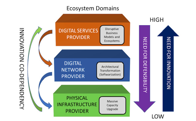
The position paper describes the telecommunications ecosystem in three layers (see diagram).
The CSPs are examples of the physical infrastructure providers (bottom layer) that have fixed and wireless infrastructure providing connectivity. The physical infrastructure layer is where the telcos have their value – their ‘centre of gravity’ – and this won’t change, says Clarke.
The infrastructure layer also includes the access network which is the CSPs’ crown jewels.
“The telcos will always defend and upgrade that asset,” says Clarke, adding that the CSPs have never cut access R&D budgets. Access is the part of the network that accounts for the bulk of their spending. “Innovation in access is happening all the time but it is never fast enough.”
The middle, digital network layer is where the nodes responsible for switching and routing reside, as do the NFV and software-defined networking (SDN) functions. It is here where innovation is needed most.
Clarke points out that the middle and upper layers are blurring; they are shown separately in the diagram for historical reasons since the CSPs own the big switching centres and the fibre that connect them.
But the hyperscalers – with their data centres, fibre backbones, and NFV and SDN expertise – play in the middle layer too even if they are predominantly known as digital service providers, the uppermost layer.
The position paper’s goal is to address how CSPs can better address the upper two network layers while also attracting smaller players and start-ups to fuel innovation across all three.
Paper proposal
The paper identifies several key issues that curtail innovation in telecoms.
One is the difficulty for start-ups and small companies to play a role in telecoms and build a business.
Just how difficult it can be is highlighted by the closure of SDN-controller specialist, Lumina Networks, which was already engaged with two leading CSPs.
In a Telecom TV panel discussion about innovation in telecoms, that accompanied the paper’s publication, Andrew Coward, the then CEO of Lumina Networks, pointed out how start-ups require not just financial backing but assistance from the CSPs due to their limited resources compared to the established systems vendors.
It is hard for a start-up to respond to an operator’s request-for-proposals that can be thousands of pages long. And when they do, will the CSPs’ procurement departments consider them due to their size?
Coward argues that a portion of the CSP’ capital expenditure should be committed to start-ups. That, in turn, would instill greater venture capital confidence in telecoms.
The CSPs also have ‘organisational inertia’ in contrast to the hyperscalers, says Clarke.
“Big companies tend towards monocultures and that works very well if you are not doing anything from one year to the next,” he says.
The hyperscalers’ edge is their intellectual capital and they work continually to produce new capabilities. “They consume innovative brains far faster and with more reward than telcos do, and have the inverse mindset of the telcos,” says Clarke.
The goals of the innovation initiative are to get CSPs and the hyperscalers – the key digital service providers – to work more closely.
“The digital service providers need to articulate the importance of telecoms to their future business model instead of working around it,” says Clarke.
Clarke hopes the digital service providers will step up and help the telecom industry be more dynamic given the future of their businesses depend on the infrastructure improving.
In turn, the CSPs need to stand up and articulate their value. This will attract investors and encourage start-ups to become engaged. It will also force the telcos to be more innovative and overcome some of the procurement barriers, he says.
Ultimately, new types of collaboration need to emerge that will address the issue of innovation.
Next steps
Work has advanced since the paper was published in June and additional players have joined the initiative, to be detailed soon.
“This is the beginning of what we hope will be a much more interesting dialogue, because of the diversity of players we have in the room,” says Clarke. “It is time to wake up, not only because of the need for innovation in our industry but because we are an innovation retardant everywhere else.”
Further information:
Telecom TV’s panel discussion: Part 2, click here
Tom Nolle’s response to the Accelerating Innovation in the Telecommunications Arena paper, click here

Habana Labs unveils its AI processor plans
Start-up Habana Labs has developed a chip architecture that promises to speed up the execution of machine-learning tasks.
The Israeli start-up came out of secrecy in September to announce two artificial intelligence (AI) processor chips. One, dubbed Gaudi, is designed to tackle the training of large-scale neural networks. The chip will be available in 2019.
 Eitan MedinaGoya, the start-up’s second device, is an inference processor that implements the optimised, trained neural network.
The Goya chip is already in prospective customers’ labs undergoing evaluation, says Eitan Medina, Habana’s chief business officer.
Habana has just raised $75 million in a second round of funding, led by Intel Capital. Overall, the start-up has raised a total of $120 million in funding.
Deep learning
Deep learning in a key approach used to perform machine learning. To perform deep learning, use is made of an artificial neural network with many hidden layers. A hidden layer is a layer of nodes found between the neural network’s input and output layers.
To benefit from deep learning, the neural network must first be trained with representative data. This is an iterative and computationally-demanding process.
The computing resources used to train the largest AI jobs has been doubled every 3.5 months since 2012
Once trained, a neural network is ready to analyse data. Common examples where trained neural networks are used include image classification and for autonomous vehicles.
 Source: Habana Labs
Two types of silicon are used for deep learning: general-purpose server CPUs such as from Intel and graphics processing units (GPUs) from the likes of Nvidia.
Most of the growth has been in the training of neural networks and this is where Nvidia has done very well. Nvidia has a run rate close to $3 billion just building chips to do the training of neural networks, says Karl Freund, senior analyst, HPC and deep learning at Moor Insights & Strategy. “They own that market.”
Now custom AI processors are emerging from companies such as Habana that are looking to take business from Nvidia and exploit the emerging market for inference chips.
“Use of neural networks outside of the Super Seven [hyperscalers] is still a nascent market but it could be potentially a $20 billion market in the next 10 years,” says Freund. “Unlike in training where you have a very strong incumbent, in inference - which could be a potentially larger market - there is no incumbent.”
This is where many new chip entrants are focussed. After all, it is a lot easier to go after an emerging market than to displace a strong competitor such as Nvidia, says Freund, who adds that Nvidia has its own inference hardware but it is suited to solving really difficult problems such as autonomous vehicles.
“For any new processor architecture to have any justification, it needs to be significantly better than previous ones,” says Medina.
Habana cites the ResNet-50 image classification algorithm to highlight its silicon’s merits. ResNet-50 refers to a 50-layer neural network that makes use of a technique called residual learning that improves the efficacy of image classification.
Habana’s Goya HL-1000 processor can classify 15,000 images-per-second using ResNet-50 while Nvidia’s V100 GPU classifies 2,657and Intel’s dual-socket Platinum 8180 CPU achieves 1225 images-per-second.
“What we have architected is fundamentally better than CPUs and GPUs in terms of processing performance and the processing-power factor,” says Medina.
“Habana appears to be one of the first start-ups to bring an AI accelerator to the market, that is, to actually deliver a product for sale,” says Linley Gwennap, president and principal analyst of The Linley Group.
Both Habana and start-up Graphcore expect to have final products for sale this year, he says, while Wave Computing, another start-up, expects to enter production early next year.
“It is also impressive that Habana is reporting 5-6x better performance than Nvidia, whereas Graphcore’s lead is less than 2x,” says Gwennap. “Graphcore focuses on training, however, whereas the Goya chip is for inference.”
Habana appears to be one of the first start-ups to bring an AI accelerator to the market
Gaudi training processor
Habana’s Gaudi chip is a neural-network training processor. Once trained, the neural network is optimised and loaded into the inference chip such as Habana’s Goya to implement what has been learnt.
“The process of getting to a trained model involves a very different compute, scale-out and power-envelopment environment to that of inference,” says Medina.
To put this in perspective, the computing resources used to train the largest AI jobs has been doubled every 3.5 months since 2012. The finding, from AI research company OpenAI, means that the computing power being employed now has grown by over one million times since 2012.
Habana remains secretive about the details of its chips. It has said that the 16nm CMOS Gaudi chip can scale to thousands of units and that each device will have 2 terabits of input-output (I/O). This contrasts with GPUs used for training that do have scaling issues, it says.
First, GPUs are expensive and power-hungry devices. The data set used for training such as for image classification needs to be split across the GPUs. If the number of images - the batch size - given to each one is too large, the training model may not converge. If the model doesn't converge, the neural network will not learn to do its job.
In turn, reducing the batch size affects the overall throughput. “GPUs and CPUs want you to feed them with a lot of data to increase throughput,” says Medina.
Habana says that unlike GPUs, its training processor’s performance will scale with the number of devices used.
“We will show with the Gaudi that we can scale performance linearly,” says Medina. “Training jobs will finish faster and models could be much deeper and more complex.”
 The Goya IC architecture. Habana says this is a general representation of the chip and what is shown is not the actual number of tensor processor cores (TPCs). Source: Habana Labs
Goya inference processor
The Goya processor comprises multiple tensor processor cores (TPCs), see diagram. Habana is not saying how many but each TPC is capable of processing vectors and matrices efficiently using several data types - eight-, 16- and 32-bit signed and unsigned integers and 32-bit floating point. To achieve this, the architecture used for the TPC is a very-long-instruction-word, (VLIW) single-instruction, multiple-data (SIMD) vector processor. Each TPC also has its own local memory.
Other on-chip hardware blocks include a general-purpose engine (GEMM), shared memory, an interface to external DDR4 SDRAM memory and support for PCI Express (PCIe) 4.0.
What we have architected is fundamentally better than CPUs and GPUs in terms of processing performance and the processing-power factor
Habana claims its inference chip has a key advantage when it comes to latency, the time it takes for the inference chip to deliver its answer.
Latency too is a function of the batch size - the number of jobs - presented to the device. Being able to pool jobs presented to the chip is a benefit but not if it exceeds the latency required.
“If you listen to what Google says about real-time applications, to meet the 99th percentile of real-time user interaction, they need the inference to be accelerated to under 7 milliseconds,” says Medina. “Microsoft also says that latency is incredibly important and that is why they can’t use a batch size of 64.”
Habana and other entrants are going after applications where their AI processors are efficient at real-time tasks with a batch size of one. “Everyone is focussing on what Nvidia can’t do well so they are building inference chips that do very well with low batch sizes,” says Freund.
Having a low-latency device not only will enable all sorts of real-time applications but will also allow a data centre operator to rent out the AI processor to multiple customers, knowing what the latency will be for each job.
“This will generate more revenue and lower the cost of AI,” says Medina.
AI PCIe cards
Habana is offering two PCIe 4.0 card versions of its Goya chip: one being one-slot wide and the second being double width. This is to conform to some customers that already use platforms with double-width GPU cards.
Habana’s PCIe 4.0 card includes the Goya chip and external memory and consumes around 100W, the majority of the power consumed by the inference chip.
The card’s PCIe 4.0 interface has 16 lanes (x16) but nearly all the workloads can manage with a single lane.
“The x16 is in case you go for more complicated topologies where you can split the model between adjacent cards and then we need to pass information between our processors,” says Medina.
Here, a PCIe switch chip would be put on the motherboard to enable the communications between the Goya processors.
Do start-ups have a sustainable architectural roadmap that offers innovation beyond just such single-cycle operations?
Applications
Habana has developed demonstrations of four common applications to run on the Goya cards. These include image classification, machine translation, recommendations, and the classification of text known as sentiment analysis.
The four were chosen as potential customers want to see these working. “If they are going to buy your hardware for inference, they want to make sure it can deal with any topology they come up with in future,” says Medina.
Habana says it is already engaged with customers other than the largest data centre operators. And with time, the start-up expects to develop inference chips with tailored I/O to address dedicated applications such as autonomous vehicles.
There are also other markets emerging beside data centres and self-driving cars.
“Mythic, for example, targets security cameras while other start-ups offer IP cores, and some target the Internet of Things and other low-cost applications,” says Gwennap. “Eventually, most processors will have some sort of AI accelerator built-in, so there are many different opportunities for this technology.”
Start-up challenge
The challenge facing all the AI processor start-ups, says Freund, is doing more thandeveloping an architecture that can do a multiply-accumulate operation in a single processor clock cycle, and not just with numbers but withn-dimensional matrices.
“That is really hard but eventually - give or take a year - everyone will figure it out,” says Freund.
The question for the start-ups is: do they have a sustainable architectural roadmap that offers innovation beyond just such single-cycle operations?
“What architecturally are you able to do beyond that to avoid being crushed by Nvidia, and if not Nvidia then Intel because they haven't finished yet,” says Freund.
This is what all these start-ups are going to struggle with whereas Nvidia has 10,000 engineers figuring it out, he warns.
Article updated on Nov 16 to report the latest Series B funding.
Photonics and optics: interchangeable yet different
Many terms in telecom are used interchangeably. Terms gain credibility with use but over time things evolve. For example, people understand what is meant by the term carrier [of traffic] or operator [of a network] and even the term incumbent [operator] even though markets are now competitive and 'telephony' is no longer state-run.
"For me, optics is the equivalent of electrical, and photonics is the equivalent of electronics - LSI, VLSI chips and the like" - Mehdi Asghari
Operators - ex-incumbents or otherwise - also do more that oversee the network and now provide complex services. But of course they differ from service providers such as the over-the-top players [third-party providers delivering services over an operator's infrastructure, rather than any theatrical behaviour] or internet content providers.
Google is an internet content provider but with its gigabit broadband service it is rolling out in the US, it is also an operator/ carrier/ communications service provider. And Google may soon become a mobile virtual network operator.
So having multiple terms can be helpful, adding variety especially when writing, but the trouble is it is also confusing.
Recent discussions including interviewing silicon photonics pioneer, Richard Soref, raised the question whether the terms photonics and optics are the same. I decided to ask several industry experts, starting with The Optical Society (OSA).
Tom Hausken, the OSA's senior engineering & applications advisor, says that after many years of thought he concludes the following:
-
People have different definitions for them [optics and photonics] that range all over the map.
-
I find it confusing and unhelpful to distinguish them.
-
The National Academies's report is on record saying there is no difference as far as that study is concerned.
-
That works for me.
Michael Duncan, the OSA's senior science advisor, puts the difference down to one of cultural usage. "Photonics leans more towards the fibre optics, integrated optics, waveguide optics, and the systems they are used in - mostly for communication - while optics is everything else, especially the propagation and modification of coherent and incoherent light," says Duncan. "But I could easily go with Tom's third bullet point."
"Photonics does include the quantum nature, and sort of by convention, the term optics is seen to mean classical" - Richard Soref
Duncan also cites Wikipedia, with its discussion of classical optics that embraces the wave nature of light, and modern optics that also includes light's particle nature. And this distinction is at the core of the difference, without leading to an industry consensus.
"Photonics does include the quantum nature, and sort of by convention, the term optics is seen to mean classical," says Richard Soref. He points out that the website Arxiv.org categorises optics as the subset of physics, while the OSA Newsletter is called Optics & Photonics News, covering all bases.
"Photonics is the larger category, and I might have been a bit off base when throwing around the optics term," says Soref. If only everyone was as off base as Professor Soref.
"We need to remember that there is no canonical definition of these terms, and there is no recognised authority that would write or maintain such a definition," says Geoff Bennett, director, solutions and technology at Infinera. For Bennett, this is a common issue, not confined to the terms optics and photonics: "We see this all the time in the telecoms industry, and in every other industry that combines rapid innovation with aggressive marketing."
That said, he also says that optics refers to classical optics, in which light is treated as a wave, whereas photonics is where light meets active semiconductors and so the quantum nature of light tends to dominate. Examples of the latter would be photonic integrated circuits (PICs). "These contain active lasers components, semiconductor optical amplifiers and photo-detectors " says Bennett. "All of these rely on quantum effects to do their job."
"We need to remember that there is no canonical definition of these terms, and there is no recognised authority that would write or maintain such a definition" - Geoff Bennett
Bennett says that the person who invented the term semiconductor optical amplifier (SOA) was not aware of the definition because the optical amplifier works on quantum principles, the same way a laser does. "So really it should be a semiconductor photonic amplifier," he says.
"At Infinera, we seem for the most part to have abided to the definitions in terminology that we use, but I can’t say that this was a conscious decision," says Bennett. "I am sure that if our marketing department thought that photonic sounded better than optical in a given situation they would have used it."
Mehdi Asghari, vice president, silicon photonics research & development at Mellanox, says optics refers to the classical use and application of light, with light as a ray. He describes optics as having a system-level approach to it.
"We create a system of lenses to make a microscope or telescope to make an optical instrument using classical optics models or we use optical components to create an optical communication system," he says. This classical or system-level perspective makes it optics or optical, a term he prefers. "We are not concerned with the nature - particle versus wave - of light, rather its classical behaviour, be it in an instrument or a system," he says.
But once things are viewed closer, at the device level, especially devices comparable in size of photons, then a system-level approach no longer works and is replaced with a quantum approach. "Here we look at photons and the quantum behaviour they exhibit," says Asghari.
In a waveguide, be it silicon photonics (integrated devices based on silicon), a planar lightwave circuit (glass-based integrated devices), or a PIC based on III-V or active devices, the size of the structure or device used is often comparable or even smaller than the size of the photons it is manipulating, he says: "This is where we very much feel the quantum nature of light, and this is where light becomes photons - photonics - and not optics."
ADVA Optical Networking's senior principal engineer, Klaus Grobe, held a discussion with the company's physicists, and both, independently, had the same opinion.
"Both [photonics and optics] are not strictly defined," he says. "Optics clearly also includes classic school-book ray optics and the like. Photonics already deals with photons, the wave-particle dualism, and hence, at least indirectly, with quantum mechanics, and possibly also quantum electro-dynamics (QED)."
Since in fibre-optics for transport, ray-propagation models no longer can be used, and also since they rely on the quantum-mechanical behaviour, for example of diode receivers, fibre-optics are better filed under photonics, says Grobe: "But they are not called fibre-photonics".
So, the industry view seems to be that the two terms are interchangeable but optics implies the classical nature of light while photonics suggests light as particles. Which term includes both seems to be down to opinion. Some believe optics covers both, others believe photonics is the more encompassing term.
Mellanox's Asghari once famously compared photons and electrons to cats and dogs. Electrons are like dogs: they behave, stick by you and are loyal; they do exactly as you tell them, he said, whereas cats are their own animals and do what they like. Just like photons. So what is his take?
He believes optics is more general than photonics. He uses the analogy of electrical versus electronics to make his point. An electronics system or chip is still an electrical device but it often refers to the integrated chip, while an electrical system is often seen as global and larger, made up of classical devices.
"For me, optics is the equivalent of electrical, and photonics is the equivalent of electronics - LSI, VLSI chips and the like," says Asghari. "One is a subset or specialised version of the other due to the need to get specific on the quantum nature of light and the challenges associated with integration."
"Optics refers to all types of cats, be it the tiger or the lion or the domestic pet. Photonics refers to the so called domestic cat that has domesticated and slaved us to look after it" - Mehdi Asghari
To back up his point, Ashgari says take a look at older books and publications that use the term optics. The term photonics started to be used once integration and size reduction became important, just as how electrical devices got replaced with electronic devices.
Indeed, this rings true in the semiconductor industry: microelectronics has now become nano-electronics as CMOS feature sizes have moved from microns to nanometer dimensions.
And this is why optical fibre or the semiconductor optical amplifier are used because these terms were invented and used when the industry was primarily engaged with the use of light at a system level and away from the quantum limits and challenges of integration.
"In short, photonics is used when we acknowledge that light is made of photons with all the fun and challenges that photons bring to us and optics is when we deal with light at a system level or a classical approach is sufficient," says Asghari.
Happily, cats and dogs feature here too.
"Optics refers to all types of cats, be it the tiger or the lion or the domestic pet," says Asghari. "Photonics refers to the so called domestic cat that has domesticated and slaved us to look after it."
Last word to Infinera's Bennett: "I suppose the moral is: be aware of the different meanings, but don’t let it bug you when people misuse them."
Books in 2013 - Part 1
Gazettabyte is asking various industry figures to highlight books they have read this year and recommend, both work-related and more general titles.
Part 1:
Tiejun J. Xia (TJ), Distinguished Member of Technical Staff, Verizon
The work-related title is Optical Fiber Telecommunications, Sixth Edition, by Ivan Kaminow, Tingye Li and Alan E. Willner. This edition, published in 2013, includes almost all the latest development results of optical fibre communications.
My non-work-related book is Fortune: Secrets of Greatness by the editors of Fortune Magazine. While published in 2006, the book still sheds light on the 'secrets' of people with significant accomplishments.
Christopher N. (Nick) Del Regno, Fellow Verizon
OpenStack Cloud Computing Cookbook, by Kevin Jackson is my work-related title. While we were in the throes of interviewing candidates for our open Cloud product development positions, I figured I had better bone up on some of the technologies.
One of those was OpenStack’s Cloud Computing software. I had seen recommendations for this book and after reading it and using it, I agree. It is a good 'OpenStack for Dummies' book which walks one through quickly setting up an OpenStack-based cloud computing environment. Further, since this is more of a tutorial book, it rightly assumes that the reader would be using some lower-level virtualisation environment (e.g., VirtualBox, etc) in which to run the OpenStack Hypervisor and virtual machines, which makes single-system simulation of a data centre environment even easier.
Lastly, the fact that it is available as a Kindle edition means it can be referenced in a variety of ways in various physical locales. While this book would work for those interested in learning more about OpenStack and virtualisation, it is better suited to those of us who like to get our hands dirty.
My somewhat work-related suggestions include Brilliant Blunders: From Darwin to Einstein – Colossal Mistakes by Great Scientists That Changed Our Understanding of Life and the Universe, by Mario Livio.
I discovered this book while watching Livio’s interview on The Daily Show. I was intrigued by the subject matter, since many of the major discoveries over the past few centuries were accidental (e.g. penicillin, radioactivity, semiconductors, etc). However, this book's focus is on the major mistakes made by some of the greatest minds in history: Darwin, Lord Kelvin, Pauling, Hoyle and Einstein.
It is interesting to consider how often pride unnecessarily blinded some of these scientists to contradictions to their own work. Further, this book reinforces my belief of the importance of collaboration and friendly competition. So many key discoveries have been made throughout history when two seemingly unrelated disciplines compare notes.
Another is Beyond the Black Box: The Forensics of Airplane Crashes, by George Bibel. As a frequent flyer and an aviation buff since childhood, I have always been intrigued by the process of accident investigation. This book offers a good exploration of the crash investigation process, with many case studies of various causes. The book explores the science of the causes and the improvements resulting from various accidents and related investigations. From the use of rounded openings in the skin (as opposed to square windows) to high-temperature alloys in the engines to ways to mitigate the impact of crash forces on the human body, the book is a fascinating journey through the lessons learned and the steps to avoid future lessons.
While enumerating the ways a plane could fail might dissuade some from flying, I found the book reassuring. The application of the scientific method to identifying the cause of, and solution to, airplane crashes has made air travel incredibly safe. In exploring the advances, I’m amazed at the bravery and temerity of early air travelers.
Outside work, my reading includes Doctor Sleep, by Stephen King. The sequel to “The Shining” following the little boy (Dan Torrence) as an adult and Dan’s role-reversal now as the protective mentor of a young child with powerful shining.
I also recommend Joyland (Hard Case Crime), by Stephen King. King tries his hand at writing a hard-case crime novel with great results. Not your typical King…think Stand by Me, Hearts in Atlantis, Shawshank Redemption.
Andrew Schmitt, Principal Analyst, Optical at Infonetics Research
My work-related reading is Research at Google.
Very little signal comes out of Google on what they are doing and what they are buying. But this web page summarises public technical disclosures and has good detail on what they have done.
There are a lot of pretenders in the analyst community who think they know the size and scale of Google's data center business but the reality is this company is sealed up tight in terms of disclosure. I put something together back in 2007 that tried to size 10GbE consumption (5,000 10GbE ports a month ) but am the first to admit that getting a handle on the magnitude of their optical networking and enterprise networking business today is a challenge.
Another offending area is software-defined networking (SDN). Pundits like to talk about SDN and how Google implemented the technology in their wide area network but I would wager few have read the documents detailing how it was done. As a result, many people mistakenly assume that because Google did it in their network, other carriers can do the same thing - which is totally false. The paper on their B4 network shows the degree of control and customisation (that few others have) required for its implementation.
I also have to plug a Transmode book on packet-optical networks. It does a really good job of defining what is a widely abused marketing term, but I’m a little biased as I wrote the forward. It should be released soon.
The non-work-related reading include Nate Silver’s book: The Signal and the Noise: Why So Many Predictions Fail — but Some Don't . I am enjoying it. I think he approaches the work of analysis the right way. I’m only halfway through but it is a good read so far. The description on Amazon summarises it well.
But some very important books that shaped my thinking are from Nassim Taleb . Fooled by Randomness is by far the best read and most approachable. If you like that then go for The Black Swan. Both are excellent and do a fantastic job of outlining the cognitive biases that can result in poor outcomes. It is philosophy for engineers and you should stop taking market advice from anyone who hasn’t read at least one.
The Steve Jobs biography by Walter Isaacson was widely popular and rightfully so.
A Thread Across the Ocean is a great book about the first trans-Atlantic cable, but that is a great book only for inside folks – don’t talk about it with people outside the industry or you’ll be marked as a nerd.
If you are into crazy infrastructure projects try Colossus about the Hoover Dam and The Path Between the Seas about the Panama Canal. The latter discloses interesting facts like how an entire graduating class of French engineers died trying to build it – no joke.
Lastly, I have to disclose an affinity for some favourite fiction: Brave New World, by Aldous Huxley and The Fountainhead by Ayn Rand.
I could go on.
If anyone reading this likes these books and has more ideas please let me know!
Books in 2013 - Part 2, click here