
Q&A with Jerry Rawls - Part 2
The concluding part of the interview with Finisar's executive chairman and company co-founder, Jerry Rawls, to mark the company's 25th anniversary.
Second and final part

Guys that are in the silicon photonics industry have a religion. It does not make any difference what the real economics are, what the real performance is, they talk with a religious fervour about what might be possible with silicon
Q: Over 25 years, what has been one of your better decisions?
Jerry Rawls: After the crash of 2001, we asked what are we going to do in the optics business? Are we going to stay in it? Is there a bright future? And if so, how are we going to respond to it?
We still believed that this was an attractive market and we had built an important brand. And, we knew we could make it more successful in the future, but we were going to have to change the way we did business.
Deciding to become vertically integrated was the key change. At that time, every other company was trying to sell their assets and remove their fixed costs. They were outsourcing manufacturing instead of bringing it in-house. Everyone wanted a variable cost business model, not a fixed cost model. We clearly went against the mainstream.
That is one of the better decisions we ever made.
Equally, with the benefit of hindsight, what do you regret?
A couple of acquisitions that we made in our early years turned out less than desirable. We were sold some technology for which we believed the probability of success was high. We bought the companies based on their technology, not necessarily on their business, and it did not pan out. One thing we learned from those experiences is that when we buy a company, we try to be much more careful about our due diligence.
Another one I regret, although I don't think it was a bad decision: We had created a division in the company called Network Tools that was the leading company in the SAN (storage area network) industry for protocol analysis.
Every company in the world that was creating SAN equipment bought our protocol analysers for Fibre Channel. That was about a $40 million-a-year business and nicely profitable. We sold it [to JDSU] in 2009 and I regret that because we started that business from scratch. It really helped create the SAN industry; it helped our customers prove their equipment interoperability.
We sold it because we had that $250 million in debt we had to pay off. We had borrowed the money and it was now due. It [2009] was still not a great time, we were trying to raise cash and one asset that had value was this division.

How would you describe the current state of the optical component industry and the main challenges it faces?
The optical component industry is in a pretty healthy place. For the most part, the larger companies are doing quite well. Our business is doing nicely. We have had four quarters in a row where revenues have grown, our profitability metrics are improving and our outlook is good. A lot of that has to do with our focus on the data centre market.
We anticipate increasing dollars spent worldwide by phone companies over the next five years
The speeds and feeds in data centres are increasing dramatically: data centres are becoming larger, the connections are faster - connections that used to be copper back in the days of Gigabit Ethernet are now at 10 Gigabits and mostly optical. That transformation of copper to optics that took place in the telephone world 35 years ago is now in full bloom in the data centres. So it is a great time to be in optics because the trends are rolling our way.
We are anticipating spending growth in the telecommunications world with an upgrade in global networks to deal with growing Internet traffic. These networks are changing to very sophisticated ROADM [reconfigurable optical add/drop multiplexer] architectures and 100 Gigabit transmission rates.
We anticipate increasing dollars spent worldwide by phone companies over the next five years. So that sector is going to become healthier and hopefully a larger percentage of our business.
I believe the optical component industry has a number of market opportunities that are going to keep it pretty healthy for some time.
It does not mean that we don't have challenges. The industry, and in particular telecommunications, is fragmented. There are a number of competitors that have very small market share. Many of these competitors are focussing their R&D efforts on the same products - the next generation of telecom equipment - and that is very inefficient. That is the main challenge that the optical industry has, that this fragmentation leads to inefficiency.
That limits the margins of the companies and the industry. It also means that pricing in the industry is at a lower level than component suppliers would like to see.
How that works out is not clear. You could say that in a fragmented industry, you would like to see more consolidation. There will be a little of that. But there are some parts of the industry where consolidation will be very slow.
For example, all of the Japanese optical suppliers are likely to stay in business for some time. Almost every big Japanese electronics company has an optical division, and they always have. None went out of business in the crash of '01 and none went out in the crash of '08 – ’09. That is because these optics divisions are small parts of giant conglomerates. This fragmentation problem is difficult to solve.
Datacom and the data centre appear to be a more interesting segment in terms of driving change than telecom. How do you view the two segments going forward?
I think both are interesting.
The data centre is interesting because of the increased density of Gigabits-per-square-inch on the faceplates of equipment, whether it is switches, storage or servers. Then there is the faster connection speeds between devices and the demand for low latency. The physical size of some of these data centres is demanding that certain connections become single mode - more like wiring a campus as opposed to multi-mode historically used in single buildings.
The datacom market is also very interesting because of a number of connections changing from copper to optical as speeds get faster. Copper transmission demands too much power through big cables at these higher speeds.
In telecom, today what is really exciting is the advent of coherent transmission systems, in particular at 100 Gigabits moving to 400 Gigabit and 1 Terabit-per-second in the next decade.
Coherent transmission is revolutionary in that by using electronics rather than optics to do signal correction for long distance fibre transmission, these signals can be much more efficient, run faster and be much less costly than they have ever been in the past.
Coupled with that is the automation of these optical networks through the extensive use of sophisticated ROADMs. With the next generation of networks, truck rolls to do provisioning and reconfigurations will be almost eliminated.
So there is a lot of excitement for us just because of what is coming to telecom networks. We have been through a lull for the last couple of years but it is a cyclical industry that tends to follow technology waves. We are entering the 100 Gigabit transmission wave and the sophisticated use of many, many ROADMs in these networks for automation.
We have designed silicon photonic chips here at Finisar and have evaluations that are ongoing
Silicon photonics is spoken of as a disruptive technology for datacom and telecom. It also promises to disrupt the component supply chain. What is Finisar's take on the technology?
As a company, we are very product focussed and we want to deliver transmission products and switching products, etc. that fulfill our customers' needs. We don't really care what the technology is. We are going to invest in technology that enables us to build the highest performing and most efficient devices that we can.
Silicon photonics is an interesting technology. We haven't used it in any of our products so far with the exception of a silicon waveguide in an integrated receiver. The most interesting thing about silicon photonics is not just to be able to make waveguides for multiplexers or demultiplexers, but to make modulators.
People have been speculating for years that we will have to use external modulators to achieve higher transmission speeds as we won’t be able to directly drive a laser fast enough.
We make VCSELs by the tens of millions. When we were making them at one Gigabit-per-second [Gbps], there were those in the industry that predicted that we would never be able to run at 2 Gbps as it would be impossible to modulate the lasers that fast. Then we did 2 Gbps, and then there were those that said it would be impossible to do 4, 8 or 10 Gigabits. Well, we are shipping devices today that are 25Gbps VCSELs that are directly modulated.
At every one of those steps there were people investing in silicon photonics companies because they could build modulators they thought would run that fast. I believe every one of those silicon photonics companies went broke.
We now have a new wave of silicon photonics companies. And because Cisco Systems happened to buy one [LightWire], there has been a lot of excitement about silicon photonics.
Well, the physics are such that it is always more efficient to directly modulate a laser - that is, to drive it with an injection of current - than it is to have a continuous wave laser where you externally modulate the light. The external modulation takes more power, more components and more cost.
Guys that are in the silicon photonics industry have a religion. It does not make any difference what the real economics are, what the real performance is, they talk with a religious fervor about what might be possible with silicon.
To date, no one has been able to make light out of silicon. That means one can make a silicon modulator and a silicon waveguide but still have to buy an indium phosphide laser to create light. Then they would have to bond that laser to the silicon substrate in a way that it efficiently launches light, is mechanically stable, and hermetic and that it will stand the rigours of all these networks. That means it can be deployed for 10 or 20 years over temperatures of 0 to 85 degrees C, and survive the qualification torture tests of high humidity, high heat and temperature cycling.
One of the things in the silicon photonics industry to date has been that the packaging - and therefore the yields - have been so difficult, such that the costs have been very high.
I promise you today that for almost every application, silicon photonics costs are higher than using traditional indium phosphide and gallium arsenide lasers and direct modulation.
We don't ignore silicon photonics as a potential technology.
We have designed silicon photonic chips here at Finisar and have evaluations that are ongoing. There are many companies that now offer silicon photonics foundry services. You can lay out a chip and they will build it for you.
We can go to a foundry; we can use their design rules and libraries and design silicon modulators and waveguides and put together a chip with as many splits and Mach-Zehnders that we want. The problem is we haven't found a place where it can be as efficient or offer the performance as using traditional lasers and free-space optics.
Our packaging has been more efficient and our output has been at a higher performance level. Remember that silicon is optically quite lossy. That means you have to launch a lot of light into it to get a little light out.
So far we just haven't found a product where we thought silicon photonics modulation was as efficient as we could build using some other technology. That is true today.
We may use silicon photonics one of these days. In fact, if we look back five or 10 years ago, when we predicted what we would need to build a 100 Gig transponder, silicon photonics was one of our alternatives, and one of the paths we went down in parallel in completing the design.
As it turns out, traditional optics and micro-optical components exceeded our own expectations.
I compare it to the disc drive industry. Twenty years ago people were predicting the demise of the disc drive industry because of solid state memory. It was thought impossible that disc drives would be around five years hence. Well, the guys in the disc industry learned how to increase the bit density and the resolution of the heads and look at the industry today. You can buy a Terabyte drive for less than a hundred dollars. The amazing technology advances they have made have kept them in the game.
What are the biggest challenges facing Finisar?
The biggest challenge we face is meeting the changes in the industry. The use of information is becoming so pervasive - video everywhere and 4G networks - that means all the kids are going to be streaming HD video to some device in their hand. And there is going to be billions of them.
Also, another challenge is managing the expectations of our customers - the equipment companies - in terms of delivering the speeds, densities and the low power performance needed to provide all this information.
It is a daunting task.
We have customers today trying to design systems that will have Terabit-per-second optical links. We don't know how we are going to get there yet but I promise you we will.
The industry in 25 years' time: Still datacom & telecom or something else by then?
In 25 years' time, datacom and telecom will be much more converged.
The data center today is becoming more like wiring a campus network than it is wiring a building as the distances become larger and the speeds faster. Today in data centers we only use point-to-point connections; we use no multiple wavelengths on fibres.
In the telephone world, everything is WDM. Today we are using mostly 96 wavelengths on a single fibre. Those 96 channels can all run at 100 Gbps – a total of nearly 10 Terabit on a single fiber. In the data center world most connections are single wavelengths, point-to-point. But in 25 years, the data centers are going to be using many of the techniques that are used in the telecom networks today in terms of making efficient use of fibres, using multiple colors of light, and being able to switch those individual colours.
For the first part, click here
Interview with Finisar's Jerry Rawls
Finisar is celebrating its 25th anniversary. Gazettabyte interviewed Finisar's executive chairman and company co-founder, Jerry Rawls, to mark the anniversary.
Part 1
 Jerry Rawls, Finisar's executive chairman and co-founder
Q: How did you meet fellow Finisar co-founder Frank Levinson?
JR: I was a general manager of a division at Rachem, a company in Menlo Park, California. We were developing and manufacturing electric interconnect products; our markets were mostly defence electronics and the computer industry.
Our customers were starting to talk a lot about fibre optics and we had no products. It seemed like it was going to be a hole in our portfolio. So I started a fibre optics product development group and hired a bright young physicist from Bell Labs to be the principal technologist. His name was Frank Levinson.
What decided you both to set up Finisar?
The division I was running was very successful: we were the fastest growing and the most profitable. Frank was lured away by our chairman to work on a fibre-optics start-up that was internally funded: Raynet.
Raynet lost almost a billion dollars over the next few years. It was the biggest venture loss in the history of Silicon Valley, and it may still be the biggest venture capital loss in Silicon Valley history.
At they were losing money, and it was sucking money from the rest of the company, our division was unable to fund a lot of projects we would have liked to have funded if we were to continue to grow. Frank was very frustrated as they were jousting at windmills.
We had lunch one day and talked about the possibility of starting a fibre-optics company. It was as simple as that: we could do better on our own. This was in 1987.
What convinced you both that high-speed fibre optics was a business to pursue?
 Frank LevinsonFrank had some original patents from Bell Labs on wavelength division multiplexing (WDM) and the use of fibre optics in telephony. That is where fibre optics first had a major impact.
As we started a little company, the thing that was happening in 1988 was that the Mac OS had just been introduced and Windows was right behind it. This was the first time colour and graphics were introduced to the PC. As we watched the change to graphics and colour, we knew video was not going to be too far behind. It was clear that files would be larger, and the bandwidth between systems, and between storage and systems, would need to be greater.
And so we started to think about high-speed optics for data centres. And the corollary to that was low-cost, high-speed optics for data centres.
We did not think we were up to competing with the telecommunications industry because in those days AT&T Bell Labs (Lucent), Alcatel and Nortel dominated the world of fibre optics. They built their own components, they built their own sub-systems and we did not think there was any chance of a start-up competing with them.
But in the world of computer networks, there were no established suppliers as fibre optics was almost non-existent there. Our goal was to focus on Gigabit-per-second speeds and how we could build low-cost Gigabit optical links for data centres.
The reason low cost was so important was that to buy an OC-12 (622 Megabit-per-second SONET) link, the cost was thousands of dollars at each end. This was a telephony fibre link but there was no chance you could be successful in any sort of computer installation with an optical connection at such prices.
So the question was: How do you bring the cost down and the prices down to a level that networks could afford, and that were priced lower than the computers at each end?
"Frank and I started the company with our own money. We had no outside investors. I took a second mortgage on my house and off we went to start a company"
So we looked for compromises. One was distance. OC-12s went 20km, 40km, 80km but data centres only needed a few hundred meters. Ok, if we can build a link that goes 500m, we have covered any data centre in the world.
The next thing was: What does that open up? And what can we do? It quickly led us to multi-mode transmission, and multi-mode transmission turned out for us to be much, much cheaper to build because the core of the fibre was either 50 or 62.5 microns versus 8 microns in telephony fibre. That means that the core is enormous compared to telephone fibres, and our job for alignment [with the laser] was that much easier.
We built some early samples. We went through several iterations to get there. We put together the components and ICs and we finally had a product that we thought was pretty good. We had a 1 Gigabit transmitter with 17 pins and a 1 Gigabit receiver with 17 pins, and we had a Gigabit transceiver with 28 pins.
Our first customers for these devices were the national laboratories. Lawrence Livermore National Lab was one of the pioneers in the world of Fibre Channel. They, working with IBM, had a big hand in the whole Fibre Channel protocol.
Our engagement with Lawrence Livermore led to other labs. All these physicists, building high-energy physics experiments, all of a sudden started buying these optical transceivers from us by the thousands. That was our first product.
Finisar's initial focus included consulting. What sort of things was the company doing during this period?
Consulting, we did a tiny bit. Mostly, what we did was contract design engineering.
Frank and I started the company with our own money. We had no outside investors. I took a second mortgage on my house and off we went to start a company. That meant we had to be able to support ourselves and our employees. We had to have customers that pay their bills.
 Early optical transceiver product from Finisar
So one of the things we did in the early days is we found customers to do design work for. We designed fibre optic systems, we designed cable TV fibre optics systems, we designed special fibre interconnects, we did some special fibre testing - which you might call consulting. We designed a scuba-diver computer that calculated dive tables - whether you would get the bends or not, how long you could stay down, and what depth and pressure. We designed a swimming pool chlorination control system.
We did a lot of things along the way to generate revenue to support our simultaneous product development work to build the Gigabit optics devices.
We didn't start the company to be a contract design house; we started it to be a product company. But the financial reality was we had to have enough money coming in to support our employees and ourselves.
"His firm had so much inventory of the products from that company that he didn’t think they would buy anything for the next three or four years"
In the late 1990s, Finisar experienced the optical boom and then the crash. Do you recall when you first realised all was not well?
In November and December of 2000, we were about to acquire two companies. Both were component suppliers in the telecommunications industry. They both sold to big customers like Alcatel, Nortel and Lucent.
In the due-diligence process for one of the companies, I was on a phone call with Lucent who had been a huge customer – maybe 40 percent of their business came from Lucent. Talking to the VP of procurement about his history with this company and what his company’s future prospects were - all the things you do normally do in due diligence - he confirmed what his previous business had been and that he was satisfied with them as a supplier. They were a good company.
But, as we talked about future business, he went silent. And, then he came back with some devastating news: his firm had so much inventory of the products from that company that he didn’t think they would buy anything for the next three or four years. This fact was unknown to the company we were acquiring. That was my first signal that something bad was going on.
We did not acquire this company. We were in the late stages of the acquisition discussions – talking to their customers is usually one of the last things you do in due diligence – but there was obviously a material adverse change in the outlook of this company. So, we quickly terminated discussions.
A very similar thing happened with the other company only a couple of weeks later. This was late 2000, it was clear the bell was ringing. Something bad was about to happen in the optics, telephony, networking industry.
In our January quarter of 2001, we could see the incoming order rate falling. And by our February-April quarter that year, our revenues had dropped something like 47 percent in two quarters. It rolled through the industry pretty fast.
How did Finisar navigate the turbulent aftermath?
We were in a bit in shock, as most of the industry was.
To put it in perspective, our revenues dropped 47 percent in two quarters; Nortel’s High Performance Optical Components division, which had sales in one quarter during 2000 of $1.4 billion, their revenues dropped to something like $28 million. Some 98.5 percent of their revenue disappeared, it was that disastrous a time, particularly in telecom.
The issue with Finisar was that the business we built was predominantly about computer networks. We didn’t have that much business with telecom. We were selling optics for data centres and so our business didn’t decline as much as the Nortels, Alcatels and the Lucents. But it was still a precipitous decline and so we had to decide: Were we still going to stay in this business or were we going to open a hamburger stand or some other kind of a business? And our answer was we didn’t know much about the hamburger business or any other business.
We thought that, long term, fibre optics was going to be a good business. The use of information was only going to increase and that was a place where we had built a fundamental market position and we ought to continue.
To do that, we had to change our spots, that is, change our way of doing business. We were going to have to be more cost competitive. Enormous capacity had been created in the optics industry in the '90s and that capacity didn’t all evaporate [with the bust]. We knew we were going to have to be much more cost-competitive.
We decided that our strategy was to be a vertically-integrated company. In the ‘90s we were not vertically integrated: we bought lasers from the Japanese or Honeywell who made VCSELs, we bought photo-detectors from either US or Japanese suppliers, we bought ICs from merchant semiconductor companies, and we put it all together. We even outsourced all of our assembly and manufacturing. But in the future, we were convinced that we had to be more cost-competitive.
"One of the things that I think is really important here is that we allow people to make mistakes"
During this period Finisar had an IPO. How did it impact the company and this strategy?
We had previously had an IPO in 1999 that raised some money. The first thing we did after the crash was to buy a factory in Malaysia. This was around March 2001, business had started to crash, everyone was selling, and if you were buying, you could get a pretty good deal on almost anything. So we bought this factory from Seagate – 640,000 sq. ft. of almost brand new building, with 200,000 sq. ft. of clean room, 20 acres of land – we bought it for $10 million.
Then we decided we had to be vertically integrated with our ICs. We weren’t going to start an IC foundry but we had to start an IC design group. So we hired a senior IC design manager from National Semiconductor who had led their analogue design efforts and we started a semiconductor design group. Today we design almost all of the ICs that go into our datacom products. We have some 60 people worldwide who are involved in IC design, layout, testing and verification.
Next, we bought the Honeywell VCSEL fab. They were our big supplier, we were their largest customer. Honeywell decided that that business was not strategic and so we bought it.
We also bought a small laser fab in Fremont, California to make edge-emitting lasers. We could also make photo-detectors in both those fabs. So we were now in a position we could make photo-detectors and lasers, and we could design ICs and go to foundry with them instead of buying them from merchant semiconductor companies and pay their margins.
We had a beautiful big factory we could build our products in, and expand for years to come. We are still expanding in that factory. Today we have over 5,000 employees in that plant in Malaysia.
To finance all the tomfoolery, we needed a lot more money than we were able to raise with our IPO. I went to New York and Boston and peddled a convertible bond issue for $250 million. So we raised a enough cash that we could finance these acquisitions and also support the company through this crash and downturn.
It was great we were a public company because we couldn’t raise that much money if we had been a private company. It worked out well; and we eventually paid all that debt off.
Fast-forward to today, we are targeting more than a billion dollars in revenue this year, we are the largest company in our industry and I think we are the most profitable.
In 2006 IEEE Spectrum Magazine ranked Finisar top in terms of patent power among telecom equipment manufacturers. Is this still a key strategic goal of Finisar? And if so, how do you ensure innovation continues year after year?
I wouldn’t say patents are a strategic goal of ours. The IEEE Spectrum ranking was based on the number of patents you had, how many you had issued recently, but it also was importantly weighted by how many times your patents were referenced by other patent applications. A lot of ours were referenced by others who were filing patents. We ended up pretty high on the list.
We do have over 1,000 issued US patents, and we have about 500 issued international patents. We employ maybe as many as 1,300 engineers and almost 300 of them have Ph.Ds. We will continue to innovate. We have been a leader in this industry for years. Our goal is to try to be out in front, to deliver the products that meet the speeds, the power, the density that our customers need for high-speed transmission. That means we have to have a lot of talented people, we have to be focussed. And, I promise you that innovation is very important to our success.
It is not so much about how many patents we get issued. Patents are important many times for defensive purposes as much as anything else. People can’t come after us and sue us frivolously for patent infringement because we have so many patents that cover products they likely make. In the end, patents for defence is really important.
Is there something that you have learnt over the years that has proved successful regarding innovation?
First, we want to be an innovative company. When we hire, we look for innovative people, we look for clever people, smart people, but also people with good interpersonal skills, that is a part of our culture.
But one of the things that I think is really important here is that we allow people to make mistakes. We don’t encourage people to make mistakes but we allow people to make mistakes. If they are trying to do their job and they make a mistake, we don’t fire them. We try to learn from the mistakes.
Over time, we have had guys make what appeared to be pretty serious mistakes that I am sure people might have been fired for in many other companies. But, for us, we are supportive of our employees. As long as we know they are not being lazy or dishonest, we support them.
I think that environment where you can try to innovate, you can work on projects but you know the culture of the company is not vengeful and that we will tolerate mistakes is an important part of our innovative environment.
For the second and final part, click here
Achieving 56 Gigabit VCSELs
A Q&A with Finisar's Jim Tatum, director of new product development. Tatum talks about the merits of the vertical-cavity surface-emitting laser (VCSEL) and the challenges to get VCSELs to work at 56 Gigabit.
Briefing: VCSELs
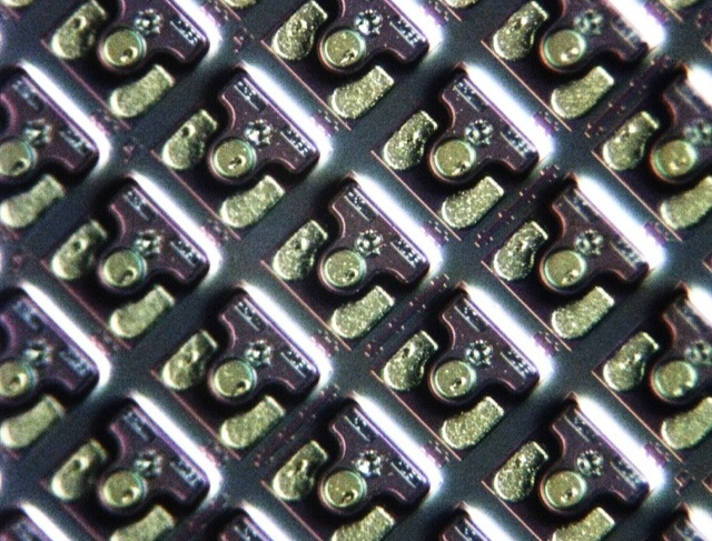 VCSELs galore! A wafer of 28 Gig devices Source: Finisar
Q. What are the merits of VCSELs compared to other laser technologies?
A: VCSELs have been a workhorse for the datacom industry for some 15 years. In that time there have been some 500 million devices deployed for data infrastructure links, with Finisar being a major producer of these VCSELs.
The competition is copper which means you need to be at a cost that makes such [optical] links attractive. This is where VCSELs have value: operating at 850nm which means running on multi-mode fibre.
Coupling VCSELs to multi-mode fibre [the core diameter] is in the tens of microns whereas it is one micron for single-mode fibre and that is where the cost is. Also with VCSELs and multi-mode fibre, we don't need optical isolators which add significant cost to the assemblies. It is not the cost of the laser die itself; the difference in terms of the link [approaches] is the cost of the optics and getting light in and out of the fibre.
There are also advantages to the VCSEL itself: wafer-level testing that allows rapid testing of the die before you commit to further packaging costs. This becomes more important as the VCSEL speed gets higher.
What are the differences with 850nm VCSELs compared to longer wavelength (1300nm and 1550nm) VCSELs?
At 850nm you are growing devices that are all epitaxial - the laser mirrors are grown epitaxially and the quantum wells are grown in one shot. At the other wavelengths, it is much harder.
People have managed it at 1300nm but it is not yet proven to be a reliable material system for getting high-speed operation. When you go to 1550nm, you are doing wafer bonding of the mirrors and active regions or you are doing more complex epitaxial processing.
That is where 850nm VCSELs has a nice advantage in that the whole thing is done in one shot; the epitaxy and the fabrication are relatively simple. You don't have the complex manufacturing of chip parts that you do at 1550nm.
What link distances are served by 850nm VCSELs?
The longest standards are for 500m. As we venture to higher speeds - 28 Gigabit-per-second (Gbps) - 100m is more the maximum. And this trend will continue, at 56Gbps I would anticipate less than 50m and maybe 25m.
The good news is that the number of links that become economically viable at those speeds grows exponentially at these shorter distances. Put another way, copper is very challenged at 56Gbps lane rates and we'll see optics and VCSEL technology move inside the chassis for board-to-board and even chip-to-chip interconnects. Such applications will deliver much higher volumes.
"Taking that next step - turning the 28Gbps VCSEL into a product - is where all the traps lie"
What are the shortest distances?
There are the edge-mounted connections and those are typically 1-5m. There is also a lot of demonstrated work with VCSELs on boards doing chip-to-chip interconnect. That is a big potential market for these devices as well.
The 28Gbps VCSEL has been demonstrated but commercial products are not yet available. It is difficult to sense whether such a device is relatively straightforward to develop or a challenge.
Achieving a 28Gbps VCSEL is hard. Certainly there have been many companies that have demonstrated a modulation capability at that speed. However, it is one thing to do it one time, another to put a reliable VCSEL product into a transceiver with everything around it.
Taking that next step - turning the 28Gbps VCSEL into a product - is where all the traps lie. That is where the bulk of the work is being done today. Certainly this year there will be 25Gbps/ 28Gbps products out in customers' hands.
"With a VCSEL, you have to fill up a volume of active region with enough carriers to generate photons and you can only put in so many, so fast. The smaller you can make that volume, the faster you can lase."
What are the issues that dictate a VCSEL's speed?
When you think about going to the next VCSEL speed, it helps to think about where we came from.
All the devices shipped, from 1 to 10 Gig, had gallium arsenide active regions. It has lots of wonderful attributes but one of its less favourable ones is that it is not the highest speed. Going to 14Gbps and 28Gbps we had to change the active region from gallium arsenide to indium gallium arsenide and that gives us an enhancement of the differential gain, a key parameter for controlling speed.
What you really want to do when you are dealing with speed is that for every incremental bit of current I give the [VCSEL] device, how much more does that translate into gain, or more photons coming out? If you can make that happen more efficiently, then the edge speed of the device increases. In other words, you don't have to deal with other parasitics - carriers going into non-recombination centres and that sort of thing; everything is going into the production of photons rather than other parasitic things.
With a VCSEL, you have to fill up a volume of active region with enough carriers to generate photons and you can only put in so many, so fast. The smaller you can make that volume, the faster you can lase.
Differential gain is a measure of the efficiency in terms of the number of photons generated by a particular carrier. If I can increase that efficiency of making photons, then my transition speed and my edge speed of the laser increases.

Shown is the chart on the y-axis is the differential gain and on the x-axis is the current density going into the part. The decay tells you that if I'm running really high currents, the differential gain is worse for indium gallium arsenide parts. So you want to operate your device with a carrier density that maximises the differential gain.
Part of that maximisation is using less carriers in smaller quantum wells so that it ramps up the curve. You want to operate at a lower current density while also doing a better job of each carrier transitioning into photons.
What else besides differential gain dictates VCSEL performance?
The speed of the laser increases above threshold as the square root of the current. That gives you a return-on-investment in terms of how much current you put into the device.
However, the reliability of the part degrades with the cube of the current you put into it. So you get to a boundary condition where speed varies as the square root of the current and you have the reliability which is degrading with the cube of the current. The intersection of those two points is where you are willing to live in terms of reliability.
That is the trade-off we constantly have to deal with when designing lasers for high speed communications.
Having explained the importance of this region of operation, what changes in terms of the laser when operating at 28Gbps and at 56Gbps?
At 14Gbps and even at 28Gbps the lasers are directly modulated with little analogue trickery. That said, 28Gbps Fibre Channel does allow you to use equalisation at the receiver.
My feeling today is that at 56Gbps, direct modulation of the laser is going to be pretty tricky. At that speed there is going to have to be dispersion compensation or equalisation built into the optical system.
There are a lot of ways to incorporate some analogue or even digital methods to reduce the effective bandwidth of the device from 56Gbps to running less. One of these is a little bit of pre-emphasis and equalisation. Another way is to use analogue modulation levels. Alternatively, you can start borrowing a whole lot more from the digital communication world and look at sub-carrier multiplexing or other more advanced modulation schemes. In other words pull the bandwidth of the laser down instead of doing 1, 0 on-off stuff. At 56 Gig those things are going to be a requirement.
The bottom line is that a 28Gbps VCSEL design maybe something pretty similar to a 56 Gig part with the addition of bandwidth enhancements techniques.
"I can see [VCSEL] modulation rates going to 100Gbps"
So has VCSEL technology already reached its peak?
In terms of direct modulation of a VCSEL - pushing current into it and generating photons - 28 Gig is a reasonable place. And 56 Gig or 40Gig VCSELs may happen with some electronic trickery around it.
The next step - and even at 56Gbps - there is a fair amount of investigation of alternate modulation techniques for VCSELs.
Instead of modulating the current in the active region, you can do passive modulation of an external absorber inside the epitaxial structure. That starts to look like a modulated laser you would see in the telecom industry but it is all grown expitaxially. Once you are modulating a passive component, the modulation speed can get significantly higher. I can see modulation rates going to 100Gbps, for example.
The VCSEL roadmap isn't running out then, but it is getting more complicated. Will it take longer to achieve each device transition: from 28 to 56Gbps, and from 56Gbps to 112Gbps?
A question that is difficult to answer.
The time line will probably scale out every time you try to scale the bandwidth. But maybe not if you are able to do things like combine other technologies at 56Gbps or you do things that are more package related. For example, one way to achieve a 56 Gig link is to multiplex two lasers together on a multi-core fibre. That is significantly less challenging thing to do from a technology development point of view than lasers fundamentally capable of 56Gbps. Is such a solution cost optimised? Well, it is hard to say at this point but it may be time-to-market optimised, at least for the first generation.
Multi-core fibre is one way, another is spatial-division multiplexing. In other words, coarse WDM, making lasers at 850nm, 980nm, 1040nm - a whole bunch of different colours and multiplexing them.
There is more than one way to achieve a total aggregate throughput.
Does all this make your job more interesting, more stressful, or both?
It means I have options in my job which is always a good thing.
ECOC 2012 summary - Part 2: Finisar
Gazettabyte completes its summary of key optical announcements at the recent ECOC show held in Amsterdam. In Part 2, Finisar's announcements are detailed.
Part 2

"The general thought with system vendors is that the more they can shrink the in-line equipment into a fewer number of slots, the more slots they have open and available for revenue-generating transceiver and transponder cards"
Rafik Ward, Finisar
Finisar showed its board-mounted parallel optics module in use within a technology demonstrator from data storage firm Xyratex, showcased what it claims is the industry's first two-slot reconfigurable optical add/ drop multiplexer (ROADM) design, unveiled its first CFP2 pluggable transceiver and announced its latest WaveShaper products.
The data storage application uses Finisar's vertical-cavity surface-emitting laser (VCSEL)-based board mounted optical assembly. The optical assembly - or optical engine - comprises 24-channels, 12 transmitters and 12 receivers.
The optical engine sits on the board and is used for such applications as chip-to-chip interconnect, optical backplanes, and dense front panels, and supports a variety of protocols. These include PCI Express, Ethernet and Infiniband as well as proprietary schemes. Indeed the only limit is the VCSEL speed. The optical engine is designed to support traffic up to 28 Gigabit-per-second (Gbps) per channel, once 28 Gigabit VCSELs become available. Finisar have already demonstrated working 28Gbps VCSELs.
The ECOC demonstration showed the optical engine in use within Xyratex's demonstrator storage system. "They are carrying traffic between internal controller cards and the traffic being carried is 12-Gig SAS [serial attached SCSI]," says Rafik Ward, vice president of marketing at Finisar.
As well as the optical engine, the demonstration included polymer waveguides from Vario-optics which connect the optical engine to a backplane connector, built by Huber + Suhner, as well as SAS silicon from LSI.
Finisar first showed the waveguide and connector technologies in a demonstration at OFC 2012. "This is an early prototype but it's a very exciting one," says Ward. "It shows all elements of the ecosystem coming together and running in a live system."

Finisar also showcased what it claims is the industry's first two-slot ROADM line card. The line card was part of a Cisco Systems' platform, according to one analyst shown the demonstration.
The company-designed card uses a high port-count wavelength-selective switch (WSS) that enables both add and drop traffic. "We have built transmit and receive into the same line card using a high port-count device," says Ward. Finisar is not detailing the exact WSS used or how the system is implemented but describes it as a flexible spectrum, 2x1x17 port line card.
The advantage of a denser ROADM line card is that it frees up slots in a system vendor's chassis. A slot can be used for either in-line equipment - WSSes and amplifiers - or terminal equipment that host the transceivers and transponders.
"It is like valuable real-estate," says Ward. "The general thought with system vendors is that the more they can shrink the in-line equipment into a fewer number of slots, the more slots they have open and available for revenue-generating transceiver and transponder cards."
The company also detailed its first CFP2 100 Gigabit optical transceiver. The CFP2 uses a single TOSA comprising four distributed feedback (DFB) lasers, a shared thermo-electric cooler and the multiplexer. The CFP2 consumes under 8W by using the DFBs and an integrated transceiver optical sub-assembly (TOSA).
The CFP2 pluggable module gains industry momentum
Finisar and Oclaro unveiled their first CFP2 optical transceiver products at the recent ECOC exhibition in Amsterdam. JDSU also announced that its ONT-100G test equipment now supports the latest 100Gbps module form factor.
 Source: Oclaro
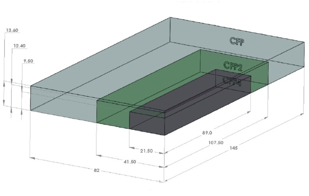
The CFP2 is the follow-on module to the CFP, supporting the IEEE 100 Gigabit Ethernet and ITU OTU4 standards. It is half the size of the CFP (see image) and typically consumes half the power. Equipment makers can increase the front-panel port density from four to eight by migrating to the CFP2.
Oclaro also announced a second-generation CFP supporting the 100GBASE-LR4 10km and OTU4 standards that reduces the power consumption from 24W to 16W. The power saving is achieved by replacing a two-chip silicon-germanium 'gearbox' IC with a single CMOS chip. The gearbox translates between the 10x10Gbps electrical interface and the 4x25Gbps signals interfacing to the optics.
The CFP2, in contrast, doesn’t include the gearbox IC.
"One of the advantages of the CFP2 module is we have a 4x25Gbps electrical interface," says Rafik Ward, vice president of marketing at Finisar. "That means that within the CFP2 module we can operate without the gearbox chip." The result is a compact, lower-power design, which is further improved by the use of optical integration.
"That 2.5x faster [interface of the CFP2] equates to about a 6x greater difficulty in signal integrity issues, microwave techniques etc"
Paul Brooks, JDSU
The transmission part of the CFP module typically comprises four externally modulated lasers (EMLs), each individually cooled. The four transmitter optical sub-assemblies (TOSAs) then interface to a four-channel optical multiplexer.
Finisar's CFP2 design uses a single TOSA holding four distributed feedback (DFB) lasers, a shared thermo-electric cooler and the multiplexer. The result of using DFBs and an integrated TOSA is that Finisar's CFP2 consumes just 8W.
Oclaro uses photonic integration on the receiver side, integrating four receiver optical sub-assemblies (ROSAs) as well as the optical demultiplexer into a single design, resulting in a 12W CFP2.
At ECOC, Oclaro demonstrated interoperability between its latest CFP and the CFP2. “It shows that the new modules will talk to existing ones,” says Robert Blum, director of product marketing for Oclaro's photonic components.
Meanwhile JDSU demonstrated its ONT-100G test set that supports the CFP2 and CFP4 MSAs.
"Initially the [test set] applications are focused on those doing the fundamental building blocks [for the 100G CFP2] – chip vendors, optical module vendors, printed circuit board developers," says Paul Brooks, director for JDSU's high speed transport test portfolio. "We will roll out more applications within the year that cover early deployment and production."
The standards-based client-side interfaces is an attractive market for test and measurement companies. For line-side optical transmission, much of the development work is proprietary such that developing a test set to serve vendors' proprietary solutions is not feasible.
The biggest engineering challenge for the CFP2 is its adoption of high-speed 25Gbps electrical interfaces. "The CFP was based on third generation, mature 10 Gig I/O [input/output]," says Brooks. "To get to cost-effective CFP2 [modules] is a very big jump: that 2.5x faster [interface] equates to about a 6x greater difficulty in signal integrity issues, microwave techniques etc."
The company says that what has been holding up the emergence of the CFP2 module has been the 104-pin connector: "The pluggable connector is the big headache," says Brooks. "The expectation is that very soon we should get some early connectors."
The test equipment also supports developers of the higher-density CFP4 module, and other form factors such as the QSFP2.
JDSU will start shipping its CFP2 test equipment in the first quarter of 2013.
Oclaro's second-generation CFP and the CFP2 transceivers are sampling, with volume production starting in early 2013.
Finisar's CFP2 LR4 product will sample in 2012 and enter volume production in 2013.
100 Gigabit direct detection gains wider backing
More vendors are coming to market with 100 Gigabit direct detection products for metro and private networks.
The emergence of a second de-facto 100 Gigabit standard, a complement to 100 Gigabit coherent, has gained credence with 4x28 Gigabit-per-second (Gbps) direct detection announcements from Finisar and Oclaro, as well as backing from system vendor, ECI Telecom.
"We believe that in some cases operators will prefer to go with this technology instead of coherent"
Shai Stein, CTO, ECI Telecom
ECI Telecom and chip vendor MultiPhy announced at OFC/NFOEC that they have been collaborating to develop a 168-pin MSA, 5x7-inch 100 Gigabit-per-second (Gbps) direct detection module. Finisar and Oclaro used the show held in Los Angeles to announce their market entry with 100Gbps direct detection CFP pluggable optical modules.
Late last year ADVA Optical Networking announced the industry's first 100Gbps direct detection product. At the same time, MultiPhy detailed its MP1100Q receiver chip designed for 100Gbps direct detection.
According to ECI, by having the 168-pin MSA interface, one line card can support a 100Gbps coherent transponder or the 100Gbps direct detection. "This is important as it enables us to fit the technology and price to the needs of end customers," says Shai Stern, CTO of ECI Telecom.
100 Gigabit transmission
Coherent technology has become the de-facto standard for 100Gbps long-haul transmission. Using dense wavelength division multiplexing (DWDM), system vendors can achieve 1,500km and greater reaches using a 50GHz channel.
But coherent designs are relatively costly and 100Gbps direct detection offers a cost-conscious alternative for metro networks and for linking data centres, achieving a reach of up to 800km.
"It [100 Gig direct detection] provides needed performance at an attractive cost, in particular when you are looking at private optical networks," says Per Hansen, vice president of product marketing, optical networks solutions at Oclaro.
Such networks need not be owned by private enterprises, they can belong to operators, says Hansen, but they are typically simple point-to-point connections or 3- to 4-node rings serving enterprises. "Bonding adjacent [4x28Gbps] wavelengths to create a 100Gbps channel that connects efficiently to your [IP] router is very attractive in such networks," says Hansen.
For more complex mesh metro networks, coherent is more attractive. "Simply because of the spectral resources being taken up through the mesh [with 4x28Gbps], and the operational aspect of routeing that," says Hansen.
ECI Telecom says that it has yet to decide whether it will adopt 100Gbps direct detection. But it does see a role for the technology in the metro since the 100Gbps technology works well alongside networks with 10 and 40 Gigabit on-off keying (OOK) channels. "We believe that in some cases operators will prefer to go with this technology instead of coherent," says Stein.
Some operators have chosen to deploy coherent over new overlay networks, to avoid the non-linear transmission effects that result from mixing old and new technologies on the one network. "With this technology, operators can stay with their existing networks yet benefit from 100 Gig high capacity links," says Stein.
Finisar says 100Gbps direct detection is also suited to low-latency applications. "The fact that it is not coherent means it doesn't include a DSP chip, enabling it to be used for low latency applications," says Rafik Ward, vice president of marketing at Finisar.
Implementation
The announced 100Gbps direct detection designs all use 4x28Gbps channels and optical duo-binary (ODB) modulation, although MultiPhy also promotes an 80km point-to-point OOK version (see Table).
 Source: Gazettabyte
The module input is a 10x10Gbps electrical interface: a CFP interface or the 168-pin line side MSA. A 'gearbox' IC is used to translate between the 10x10Gbps electrical interface and the four 28Gbps channels feeding the optics.
"There are a few suppliers that are offering that [gearbox IC]," says Robert Blum, director of product marketing for Oclaro's photonic components. AppliedMicro recently announced a duplex multiplexer-demultiplexer IC.
MultiPhy's receiver chip has a digital signal processor (DSP) that implements the maximum likelihood sequence estimation (MLSE) algorithm, which is says enables 10 Gig opto-electronics to be used for each channel. The result is a 100Gbps module based on the cost of 4x10Gbps optics. However, over-driving the 10Gbps opto-electronics creates inter-symbol interference, where the energy of a transmitted bit leaks into neighbouring signals. MultiPhy's DSP using MLSE counters the inter-symbol interference.
 100G direct detection module showing MultiPhy's MP1100Q chip. Source: MultiPhy
Oclaro and Finisar claim that using ODB alone enables the use of lower-speed opto-electronics. "This is irrespective of whether you use MLSE or hard decision," says Blum. "The advantage of using optical duo-binary modulation is that you can use 10G-type optics."
Finisar's Ward points out that by using ODB, the 100Gbps direct-detection module avoids the price/ power penalty associated with a receiver DSP running MLSE to compensate for sub-optimal optical components.
Oclaro, however, has not ruled out using MLSE in future. The company endorsed MultiPhy's MLSE device when the product was first announced but its first 100G transceiver is not using the IC.
Finisar and Oclaro's modules require 200GHz to transmit the 100Gbps signal: 4x50GHz channels, each carrying the 28Gbps signal. "This architecture will enable 2.5x the spectral efficiency of tunable XFPs," says Ward. Using XFPs, ten would be needed for a 100Gbps throughput, each channel requiring 50GHz or 500GHz in total.
MultiPhy claims that it can implement the 100Gbps in a 100GHz channel, 5x the efficiency but still twice the spectrum used for 100Gbps coherent.
Finisar demonstrated its 100Gbps CFP module with SpectraWave, a 1 rack unit (1U) DWDM transport chassis, at OFC/NFOEC. "It provides all the things you need in line to enable a metro Ethernet link: an optical multiplexer and demultiplexer, amplification and dispersion compensation," says Ward. Up to four CFPs can be plugged into the SpectraWave unit.
Operator interest
In a recent survey published by Infonetics Research, operators had yet to show interest in 100Gbps direct detection. Infonetics attributed the finding to the technology still being unavailable and that operators hadn't yet assessed its merits.
"Operators are aware of this technology," says ECI's Stein. "It is true they are waiting to get a proof-of-concept and to test it in their networks and see the value they can get.
"That is why ECI has not yet decided to go for a generally-available product: we will deliver to potential customers, get their feedback and then take a decision regarding a commercial product," says Stein.
However MultiPhy claims that this is the first technology that enables 100Gbps in a pluggable module to achieve a reach beyond 40km. That fact coupled with the technology's unmatched cost-performance is what is getting the interest. "Every time you show a potential user some way they can save on cost, they are interested," says Neal Neslusan, vice president of sales and marketing at MultiPhy.
Direct detection roadmap
Recent announcements by Cisco Systems, Ciena, Alcatel-Lucent and Huawei highlight how the system vendors will use advanced modulation and super-channels to evolve coherent to speeds beyond 100Gbps. Does direct detection have a similar roadmap?
"I don't think that this on-off keying technology is coming instead of coherent," says Stein. "Once we move to super-channel and the spectral densities it can achieve, coherent technology is a must and will be used." But for 40Gbps and 100Gbps, what ECI calls intermediate rates, direct detection extends the life of OOK and existing network infrastructure.
ECI and MultiPhy are members of the Tera Santa Consortium developing 1 Terabit coherent technology, and MultiPhy stresses that as well as its direct detection DSP chips, it is also developing coherent ICs.
Further reading: 100 Gigabit: The coming metro opportunity
Fibre-to-the-FPGA
Part 1: FPGAs
Programmable logic chip vendor Altera is developing FPGAs with optical interfaces. But is there a need for such technology and how difficult will it be to develop?
FPGAs with optical interfaces promise to simplify high-speed interfacing between and within telecom and datacom systems. Such fibre-based FPGAs, once available, could also trigger novel system architectures. But not all FPGA vendors believe optical-enabled FPGAs’ time has come, arguing that cost and reliability hurdles must be overcome for system vendors to embrace the technology
“One of the advantages of using optics is that you haven’t got to throw your backplanes away as [interface] speeds increase.”
Craig Davis, Altera
Altera announced in March that it is developing FPGAs with optical interfaces. The FPGA vendor has yet to detail its technology demonstrator but says it will do so later this year. Altera describes the advent of optically-enabled FPGAs as a turning point, driven by the speed-reach tradeoff of electrical interfaces coupled with the rising cost of elaborate printed circuit board (PCB) materials needed for the highest speed interfaces.
Interface speeds continue to rise. The Interlaken interface has a channel rate of up to 6.375 Gigabit-per-second (Gbps) while the Gen 3.0 PCI Express standard uses 8.0 Gbps lanes. Meanwhile 16 Gigabit Fibre Channel standard operates at 14.1 Gbps while 100 Gigabit interfaces for Ethernet and line-side optical transport are moving to a four-channel electrical interface that almost doubles the lane rates to 25-28 Gbps. The CFP2 optical module for 100 Gigabit, to be introduced in 2012, will use the four-channel electrical interface.
Copper interfaces such channel speeds but at the expense of reach. Craig Davis, senior product marketing engineer at Altera, cites the 10GBASE-KR 10Gbps backplane standard as an example of the bandwidth-reach the latest FPGAs can achieve: 40 inches including the losses introduced by the two connectors at each end.
“Our interactions with our customers are primarily for products that are not going to see the light of day for several years”
Panch Chandrasekaran, Xilinx
Work is being undertaken to development very short reach electrical interfaces at 28Gbps for line cards and electrical backplanes. “You are talking 4 to 6 inches of trace to a CFP2 module or a chip-to-chip interface,” says Panch Chandrasekaran, Xilinx’s senior product marketing manager, high-speed serial I/O. “Honestly, this is going to be a challenge but we usually figure out a way how to do things.”
The faster the link, the more energy has to be put into the signals and the more losses you have on the board, says Davis: “Signal integrity aspects also get more difficult, the costs go up as does the power consumption.”
According to Altera, signal losses increase 3.5x going from 10 to 30Gbps. To match the losses at 10Gbps when operating at these higher speeds, complex PCB materials such as N4000-13 EP SI and Megtron 6 are needed rather than the traditional FR4 design. However, the cost of designing and manufacturing such PCBs can rise by five-fold.
In contrast, using an optically-enabled FPGA simplifies PCB design. “For traditional chip-to-chip on a line card, optics does have a benefit because you can trade off the number of layers on a PCB,” says Davis. Such an optical-based design also offers future-proofing. “A lot of the applications we’ll be looking to support are across backplanes and between shelves,” says Davis. “One of the advantages of using optics is that you haven’t got to throw your backplanes away as [interface] speeds increase.”
FPGAs with optical interfaces also promise new ways to design systems. Normally when one line card talks to another on different shelves it is via a switch card on each shelf. Using an FPGA with an optical interface, the cards can talk directly. “People are looking at this,” says Davis. “You could take that to the extreme and go to the next cabinet which makes a much easier system design.”
Altera says vendors are interested in optical-enabled FPGAs for storage systems. Here interlinked disk drives require multiple connectors between boards. “There is an argument that it becomes a simpler system design with one FPGA taking directly to another or one chip directly to another,” says Davis “The more advanced R&D groups within certain companies are investigating the best route forward.”
But while FPGA companies agree that optical interfaces will be needed, there is no consensus on timing. “Xilinx has been looking at this technology for a while now,” says Chandrasekaran. “There is a reason why we haven’t announced it: we have a little while to go before key ecosystem and technology questions are answered.”
The mechanical and reliability issues of systems are stringent and the optical option must prove that it can deliver what is needed, says Chandrasekaran. “It is possible to do at the moment but the cost and reliability equation hasn’t been fully solved.”
Xilinx also says that while it is discussing the technology with customers, the requirement for such FPGA-based optical interfaces is some way off. “Our interactions with our customers are primarily for products that are not going to see the light of day for several years,” says Chandrasekaran
“Customers are always excited to hear about integration play,” says Gilles Garcia, director, wired communications business unit at Xilinx. But ultimately end customers care less about the technology as long as the price, power and board real-estate requirements are met. “What we are seeing with this [optical-enabled FPGA] technology is that it is not answering the requirements we are seeing from our large customers that are looking for their next-generation systems,” says Garcia
FPGA vendor Tabula also questions the near-term need for such technology. Alain Bismuth, vice president of marketing at Tabula, says nearly all the ports shipped today are at speeds of 10Gbps and below. Even in 2014, the number of 40Gbps ports forecast will only number 650,000, he says.
For Bismuth, two things must happen before optically-enabled FPGAs become commonplace. “You can build them in high volumes reliably and with good yields without incurring higher costs than a separate, discrete [FPGA and optical module] solution,” says Bismuth. “Second, the emergence in interesting volume of networks at 100 Gig and beyond to justify the integration effort.” Such networks are emerging at a “fairly slow pace”, he says.
Meanwhile Altera’s development work continues apace. “We are working with partners to develop the system and we will be demonstrating the optics-on-a-chip in Q4,” says Bob Blake, corporate and product marketing manager, Altera Europe. Altera says its packaged FPGA and optical interface will support short reach links up to 100m and be based on multimode fibre. “All we have announced is that the optical interface will be on the package and it will connect into the FPGA,” says Davis.
The technology will also use 10Gbps optical interface yet the company has detailed that its Stratix V FPGA family supports electrical transceivers at 28Gbps. “The optical interface can go higher than that [10Gbps] so in future we can target 28Gbps and beyond,” says Davis.
Optical partners
Optical component and transceiver firms such as Avago Technologies, Finisar and Reflex Photonics all have parallel optical devices - optical engines - that support up to 12 channels at 10Gbps. Avago’s MicroPod 12x10Gbit/s optical engine measures 8x8mm, for example.
None of the optical vendors would comment on its involvement with Altera’s optical-enabled FPGA.
Avago Technologies says that as FPGA interface speeds move to 10 Gbps and beyond, its customers are finding they need to move from copper to optical interfaces to maintain bandwidth for board, chassis, and system-level interconnect. “In line with this announcement from Altera, we are investing the time to verify Avago optical modules with FPGA SERDES blocks to ensure that FPGA users can design optical interfaces with confidence,” says Victor Krutul, director of marketing for fibre optic products at Avago.
Finisar too only talks about general trends. “We are seeing many technology leaders moving optics further onto the board and deeper into the system,” says Katharine Schmidtke, director of strategic marketing for Finisar. “This approach offers a number of advantages including improving signal integrity and reducing power consumption on copper traces at higher bandwidths.”
Reflex Photonics says that it has the technology and products to realise optically-enabled IC packages. “We are working with more than one IC company to bring optically-enabled IC packages to market,” says Robert Coenen, vice president, sales and marketing at Reflex.
For Coenen, FPGAs represent the first step in bringing optics to the IC package: “Due to their penetration into niche markets, FPGAs make the most sense to create what will ultimately be a huge market in optically-enabled IC packages.”
Coenen stresses that optics to the IC package is a significant shift in how optical links are used and so it will take time for this application to take hold. However, as the cost per bit decreases, optics will start being used in additional applications including switch ASICs, microprocessors and graphics processors.
“The beauty of an MT-terminated ribbon fiber optical connection at the edge of the package is that this solution allows designers to use the additional high-speed optical connectivity without having to drastically change their design practices,” says Coenen. This is not the case with technologies such as PCB optical waveguides or free-space optical communication.
“I believe the Altera announcement is just the first in what will be many announcements of optical-to-the-IC-package technology in the coming year or two,” says Coenen.
Further reading
- Briefing Part 2: Boosting high performance computing with optics
- Altera White Paper: Overcome Copper Limits with Optical Interfaces
- Xilinx's 400 Gigabit Ethernet FPGA
- The InfiniBand roadmap gets redrawn
Terabit Consortium embraces OFDM
“This project is very challenging and very important”
Shai Stein, Tera Santa Consortium
Given the continual growth in IP traffic, higher-speed light paths are going to be needed, says Shai Stein, chairman of the Tera Santa Consortium and ECI Telecom’s CTO: “If 100 Gigabit is starting to be deployed, within five years we’ll start to see links with tenfold that capacity, meaning one Terabit.”
The project is funded by the seven participating firms and the Israeli Government. According to Stern, the Government has invested little in optical projects in recent years. “When we look at the [Israeli] academies and industry capabilities in optical, there is no justification for this,” says Stern. “We went with this initiative in order to get Government funding for something very challenging that will position us in a totally different place worldwide.”
Orthogonal frequency division multiplexing
OFDM differs from traditional dense wavelength division multiplexing (DWDM) technology in how fibre bandwidth is used. Rather than sending all the information on a lightpath within a single 50 or 100GHz channel – dubbed single-carrier transmission – OFDM uses multiple narrow carriers. “Instead of using the whole bandwidth in one bulk and transmitting the information over it, [with OFDM] you divide the spectrum into pieces and on each you transmit a portion of the data,” says Stein. “Each sub-carrier is very narrow and the summation of all of them is the transmission.”
“Each time there is a new arena in telecom we find that there is a battle between single carrier modulation and OFDM; VDSL began as single carrier and later moved to OFDM,” says Amitai Melamed, involved in the project and a member of ECI’s CTO office. “In the optical domain, before running to [use] single-carrier modulation as is currently done at 100 Gigabit, it is better to look at the OFDM domain in detail rather than jump at single-carrier modulation and question whether this was the right choice in future.”
OFDM delivers several benefits, says Stern, especially in the flexibility it brings in managing spectrum. OFDM allows a fibre’s spectrum band to be used right up to its edge. Indeed Melamed is confident that by adopting OFDM for optical, the spectrum efficiency achieved will eventually match that of wireless.
“OFDM is very tolerant to rate adaptation.”
Amitai Melamed, ECI Telecom
The technology also lends itself to parallel processing. “Each of the sub-carriers is orthogonal and in a way independent,” says Stern. “You can use multiple small machines to process the whole traffic instead of a single engine that processes it all.” With OFDM, chromatic dispersion is also reduced because each sub-carrier is narrow in the frequency domain.
Using OFDM, the modulation scheme used per sub-carrier can vary depending on channel conditions. This delivers a flexibility absent from existing single-carrier modulation schemes such as quadrature phase-shift keying (QPSK) that is used across all the channel bandwidth at 100 Gigabit-per-second (Gbps). “With OFDM, some of the bins [sub-carriers] could be QPSK but others could be 16-QAM or even more,” says Melamed.
The approach enables the concept of an adaptive transponder. “I don’t always need to handle fibre as a time-division multiplexed link – either you have all the capacity or nothing,” says Melamed. “We are trying to push this resource to be more tolerant to the media: We can sense the channels' and adapt the receiver to the real capacity.” Such an approach better suits the characteristics of packet traffic in general he says: “OFDM is very tolerant to rate adaptation.”
The Consortium’s goal is to deliver a 1 Terabit light path in a 175GHz channel. At present 160, 40Gbps can be crammed within the a fibre's C-band, equating to 6.4Tbps using 25GHz channels. At 100Gbps, 80 channels - or 8Tbps - is possible using 50GHz channels. A 175GHz channel spacing at 1Tbps would result in 23Tbps overall capacity. However this figure is likely to be reduced in practice since frequency guard-bands between channels are needed. The spectrum spacings at speeds greater than 100Gbps are still being worked out as part of ITU work on "gridless" channels (see OFC announcements and market trends story).
ECI stresses that fibre capacity is only one aspect of performance, however, and that at 1Tbps the optical reach achieved is reduced compared to transmissions at 100Gbps. “It is not just about having more Gigabit-per-second-per-Hertz but how we utilize the resource,” says Melamed. “A system with an adaptive rate optimises the resource in terms of how capacity is managed.” For example if there is no need for a 1Tbps link at a certain time of the day, the system can revert to a lower speed and use the spectrum freed up for other services. Such a concept will enable the DWDM system to be adaptive in capacity, time and reach.
Project focus
The project is split between digital and analogue, optical development work. The digital part concerns OFDM and how the signals are processed in a modular way.
The analogue work involves overcoming several challenges, says Stern. One is designing and building the optical functions needed for modulation and demodulation with the accuracy required for OFDM. Another is achieving a compact design that fits within an optical transceiver. Dividing the 1Tbps signal into several sub-bands will require optical components to be implemented as a photonic integrated circuit (PIC). The PIC will integrate arrays of components for sub-band processing and will be needed to achieve the required cost, space and power consumption targets.
Taking part in the project are seven Israeli companies - ECI Telecom, the Israeli subsidiary of Finisar, MultiPhy, Civcom, Orckit-Corrigent, Elisra-Elbit and Optiway- as well as five Israeli universities.
 Two of the companies in the Consortium
“There are three types of companies,” says Stern. “Companies at the component level – digital components like digital signal processors and analogue optical components, sub-systems such as transceivers, and system companies that have platforms and a network view of the whole concept.”
The project goal is to provide the technology enablers to build a terabit-enabled optical network. A simple prototype will be built to check the concepts and the algorithms before proceeding to the full 1Terabit proof-of-concept, says Stern. The five Israeli universities will provide a dozen research groups covering issues such as PIC design and digital signal processing algorithms.
Any intellectual property resulting from the project is owned by the company that generates it although it will be made available to any other interested Consortium partner for licensing.
Project definition work, architectures and simulation work have already started. The project will take between 3-5 years but it has a deadline after three years when the Consortium will need to demonstrate the project's achievements. “If the achievements justify continuation I believe we will get it [a funding extension],” says Stern. “But we have a lot to do to get to this milestone after three years.
Project funding for the three years is around US $25M, with the Israeli Office of the Chief Scientist (OCS) providing 50 million NIS (US $14.5M) via the Magnet programme, which ECI says is “over half” of the overall funding.
Further reading:
OFC announcements and market trends
More compact transceiver designs at 10, 40 and 100 Gigabit, advancements in reconfigurable optical add-drop multiplexer (ROADM) technology and parallel optical engine developments were all in evidence at this year’s OFC/NFOEC show held in Los Angeles in March.
 “MSAs are designed by committee, and when you have a committee you throw away innovation and you throw away time-to-market”
Victor Krutul, Avago Technologies
Finisar said that the show was one of the busiest in recent years. “There was an increasing system-vendor presence at OFC, and there was a lot more interest from investor analysts,” says Rafik Ward, vice president of marketing at Finisar.
Ethernet interfaces
Opnext demonstrated an IEEE 100GBASE-ER4 module design at the show, the 100 Gigabit Ethernet (GbE) standard with a 40km reach. Based on the company’s CFP-based 100GBASE-LR4 10km module, the design uses a semiconductor optical amplifier (SOA) on the receive path to achieve the extended reach. The IEEE standard calls for an SOA in front of the photo-detectors for the 100GBASE-ER4 interface.
“We don’t have that [SOA] integrated yet, we are just showing the [design] feasibility,” says Jon Anderson, director of technology programme at Opnext. The extended reach interface will be used to connect IP core routers to transport system when the two platforms reside in separate facilities. Such a 40km requirement for a 100GbE interface is not common but is an important one to meet, says Anderson.
Opnext’s first-generation LR4, currently shipping, is a discrete design comprising four discrete transmitter optical sub-assemblies (TOSAs) and four receiver optical sub-assemblies (ROSAs) and an optical multiplexer and demultiplexer. The company’s next-generation design will integrate the four lasers and the optical multiplexer into a package and will be used in future more compact CFP2 and CFP4 modules.
The CFP2 module is half the size of the CFP module and the CFP4 is a quarter. In terms of maximum power, the CFP module is rated at 32W, the CFP2 12W and the CFP4 5W. “The CFP4 is a little bit wider and longer than the QSFP,” says Anderson. The first CFP2 modules are expected to become available in 2012 and the CFP4 in 2013.
System vendors are interested in the CFP4 as they want to support over one terabit of capacity on a 15-inch faceplate. Up to 16 ports can be supported –1.6Tbps – on a faceplate using the CFP4, and using a “belly-to-belly” configuration two rows of 16 ports will be possible, says Anderson.
Finisar demonstrated a distributed feedback laser (DFB) laser-based CFP module at OFC that implements the 10km 100GBASE-LR4 standard. The adoption of DFB lasers promises significant advantages compared to existing first-generation -LR4 modules that use electro-absorption modulated lasers (EMLs). “If you look at current designs, ours included, not only do they use EMLs which are significantly more expensive, but each is in its own package and has its own thermo-electric cooler,” says Ward.
Finisar’s use of DFBs means an integrated array of the lasers can be packaged and cooled using a single thermo-electric cooler, significantly reducing cost and nearly halving the power to 12W. “Now that the power [of the DFB-based] LR4 is 12W, we can place it within a CFP2 with its 25-28 Gigabit-per-second (Gbps) electrical I/O,” says Ward.
Moving to the faster input/output (I/O) compared to the CFP’s 10Gbps I/O means that that serialiser/ deserialiser (serdes) chipset can be replaced with simpler clock data recovery (CDR) circuitry. “By the time we move to the CFP4, we remove the CDRs completely,” says Ward. “It’s an un-retimed interface.” Finisar’s existing -LR4 design already uses an integrated four-photodetector array.
An early application of the 100GbE -LR4, as with the -ER4, is linking core routers with optical transport systems in operators’ central offices. Many Ethernet switch vendors have chosen to focus their early high-data efforts at 40GbE but Finisar says the move to 100GbE has started.
Finisar argues that the adoption of DFBs will ultimately prove the cost-benefits of a 4-channel 100GbE design which faces competition from the emerging 10x10 multi-source agreement (MSA). “Everything we have heard about the 10x10 [MSA] has been around cost,” says Ward. “The simple view inside Finisar is that by the time the Gen2 100GbE module that we showed at OFC gets to market, this argument [4x25Gig vs. 10x10Gig] will be a moot point.”
 “40Gig is definitely still strong and healthy”
Jon Anderson, Opnext
By then the second-generation -LR4 module design will be cost competitive if not even lower cost than the 10x10 MSA. “If you look at optoelectronic components, at the end of the day what really drives cost is yield,” says Ward. “If we can get our yields of 25Gig DFBs down to a level that is similar to 10Gig DFB yields- it doesn’t have to match, just in the ballpark - then we have a solution where the 4x25Gig looks like a 4x10Gig solution and then I believe everyone will agree that 4x25Gig is a less expensive architecture.” Finisar expects the Gen2 CFP -LR4 in production by the first half of 2012.
Opnext demonstrated a 40GBASE- LR4 (40Gbps, up to 10km) standard in a QSFP+ module at OFC. Anderson says it is seeing demand for such a design from data centre operators and from switch and transport vendors.
Avago Technologies announced a 40Gbps QSFP+ module at OFC that implements the 100m IEEE 40GBASE-SR4. “It will interoperate with Avago’s SFP+ modules,” says Victor Krutul, director of marketing for the fibre optics division at Avago Technologies. The QSFP+ can interface to another QSFP+ module or to four 10Gbps SFP+ modules.
Avago also announced a proprietary mini-SFP+ design, 30% smaller than the standard SFP+ but which is electrically compatible. According to Krutul, the design came about following a request from one of its customers: “What it allows is the ability to have 64 ports on the front [panel] rather than 48.”
Did Avago consider making the mini-SFP+ design an MSA? “What we found with MSAs is that they are designed by committee, and when you have a committee you throw away innovation and you throw away time-to-market,” says Krutul.
Krutul was previously a marketing manager for Intel’s LightPeak before joining Avago over half a year ago.
 “There was an increasing system-vendor presence at OFC, and there was a lot more interest from investor analysts”
Rafik Ward, Finisar.
Line-side interfaces
Opnext will be providing select customers with its 100Gbps DP-QPSK coherent module for trialling this quarter. The module has a 5-inch by 7-inch footprint and uses a 168-pin connector. “We are working to try and meet the OIF spec [with regard power consumption] which is 80W.” says Anderson. “It is challenging and it may not be met in the first generation [design].”
The company is also moving its 40Gbps 2km very short reach (VSR) transponder to support the IEEE 40GBASE-FR standard within a CFP module, dubbed the “tri-rate” design. “The 40BASE-FR has been approved, with the specification building on the ITU’s 40Gig VSR,” says Anderson. “It continues to support the [OC-768] SONET/SDH rate, it will support the new OTN ODU3 40Gbps and the intermediate 40 Gigabit Ethernet.”
Opnext and Finisar are both watching with interest the emerging 100Gbps direct detection market, an alternative to 100 Gigabit coherent aimed shorter reach metro applications.
“We certainly are watching this segment and do have an interest, but we don’t have any product plans to share at this point,” says Anderson.
“The [100Gbps] direct-detection market is very interesting,” says Ward. Coherent is not going to be the only way people will deploy 100Gbps light paths. “There will be a market for shorter reach, lower performance 100 Gigabit DWDM that will be used primarily in datacentre-to-datacentre,” he says. Tier 2 and tier 3 carriers will also be interested in the technology for use in shorter metro reaches. “There is definitely a market for that,” says Ward.
Opnext also announced its small form-factor – 3.5-inch by 4.5-inch - 40Gbps DPSK module. “With a smaller form factor, the next generation could move to a CFP type pluggable,” says Anderson. “But that is if our customers are interested in migrating to a pluggable design for DPSK and DQPSK.”
Are there signs that the advent of 100 Gigabit is affecting 40Gbps uptake? “We definitely not seeing that,” says Anderson. “We are continuing to see good solid demand for both 40G line side – DPSK and DQPSK – and a lot of pull to being this tri-rate VSR.”
Such demand is not just from China but also North Ametican carriers. “40 Gig is definitely still strong and healthy,” says Anderson “But there are some operators that are waiting to see how 100G does and approved in for major build-outs.”
At 10Gbps, Opnext also had on show a tunable TOSA for use in an XFP module, while Finisar announced an 80km, 10Gbps SFP+ module. “SFP+ has become a very successful form factor at 10Gbps,” says Ward. “All the market data I see show SFP+ leads in overall volumes deployed by a significant margin.” Its success has been achieved despite being a form factor was not designed to achieve all the 10Gbps reaches required initially. This is some achievement, says Ward, since the XFP+ form factor used for 80km has a power rating of 3.5W while the 80km SFP+ has to work within a less than 2W upper limit.
Parallel Optics
Avago detailed its main parallel optic designs: the CXP module and its two optical engine designs.
The company claims it seeing much interested from high-performance computing vendors such as IBM and Fujitsu for its CXP 120 Gigabit (12x10Gbps) parallel transceiver module. Avago is sampling the module and it will start shipping in the summer.
The company also announced the status of its embedded parallel optics devices (PODs). Such parallel optic designs offer several advantages, says Krutul. Embedding the optics on the motherboard offers greater flexibility in cooling since the traditional optics is normally at the edge of the card, furthest away from the fans. Such optics also simplify high-speed signal routing on the printed circuit board since fibre is used.
Avago offers two designs – the 8x8mm MicroPod and the 22x18mm MiniPod. The 12x10Gbps MicroPods are being used in IBM’s Blue Gene computer and Avago says it is already shipping tens of thousands of the devices a month. “The [MicroPod’s] signal pins have a very tight pitch and some of our customers find that difficult to do,” says Krutul. The MiniPod design tackles this by using the MicroPod optical engine but a more relaxed pitch. At OFC, Avago said that the MiniPod is now sampling.
Gridless ROADMs
Finisar demonstrated what it claims is the first gridless wavelength-selective switch (WSS) module at the show. A gridless ROADM supports variable channel widths beyond the fixed International Telecommunication Union's (ITU) defined spacings. Such a capability enables ROADMs to support variable channel spacings that may be required for transmission rates beyond 100Gbps: 400Gbps, 1Tbps and beyond.
“We have an increasing amount of customer interest in this [FlexGrid], and from what we can tell, there is also an increasing amount of carrier interest as well,” says Ward, adding that the company is already shipping FlexGrid WSSs to customers.
Finisar is a contributing to the ongoing ITU work to define what the grid spacings and the central channels should be for future ROADM deployments. Finisar demonstrated its FlexGrid design implementing integer increments of 12.5GHz spacing. “We could probably go down to 1GHz or even lower than that,” says Ward. “But the network management system required to manage such [fine] granularity would become incredibly complicated.” What is required for gridless is a balance between making good use of the fibre’s spectrum while ensuring the system in manageable, says Ward.
Rafik Ward Q&A - final part
"Feedback we are getting from customers is that the current 100 Gig LR4 modules are too expensive"
Rafik Ward, Finisar
Q: Broadway Networks, why has Finisar acquired the company?
A: We spent quite some time talking to Broadway and understanding their business. We also talked to Broadway’s customers and the feedback we got on the technical team, the products and what this little start-up was able to accomplish was unanimously very positive.
We think what Broadway has done, for instance their EPON* stick product, is very interesting. With that product, an end user has the ability to make any SFP* port on a low-end Ethernet switch an EPON ONU* interface. This opens up a whole new set of potential customers and end users for EPON.
In reality, consumers will never have Ethernet switches with SFP ports in their house. Where we do see such Ethernet switches are in every major enterprise and many multi-dwelling units. It is an interesting technology that enables enterprises and multi-dwelling units to quickly tool-up for EPON.
* [EPON - Ethernet passive optical network, SFP - small form-factor pluggable optical transceiver, ONU - optical network unit]
Optical transceivers have been getting smaller and faster in the last decade yet laser and photo-detector manufacturing have hardly changed, except in terms of speed. Is this about to change?
Speed is one of the focus areas for the industry and will continue to be. Looking forward in a number of applications, though, we are going to hit the limit for these lasers and we are going to have to look more carefully outside of just raw laser speed to move up the data rate curve.
"We are going to hit the limit for these lasers"
A lot of this work has already started on the line side using different modulation formats and DSP* technology. Over time the question is: What happens on the client side? In future, do we look to other modulation formats on the client side? Eventually we will get there; it may take several years before we need to do things like that. But as an industry we would be foolish to think we won’t have to do this.
WDM* is going to be an increasingly important technology on the client side. We are already seeing this with the 40GBASE-LR4 and 100GBASE-LR4 standards.
* [DSP - digital signal processing, WDM - wavelength-division multiplexing]
Google gave a presentation at ECOC that argued for the need for another 100Gbps interface. What is Finisar’s view?
Feedback we are getting from customers is that the current 100 Gig LR4 modules are too expensive. We have spent a lot of time with customers helping them understand how the current LR4 standard, as is written, actually enables a very low cost optical interface, and the timeframes we believe are very quick in terms of how we can get cost down considerably on 100 Gig.  Rafik Ward (right) giving Glenn Wellbrock, director of backbone network design at Verizon Business, a tour of Finisar's labsThat was part of the details that [Finisar’s] Chris Cole also presented at ECOC.
There has certainly been a lot of media attention on the two [ECOC] presentations between Finisar and Google. This really is not so much about the quote, ‘drama’, or two companies that have a disagreement which optical interface makes more sense. It is more fundamental than that.
What it comes down to is that, as an industry, we have pretty limited resources. The best thing all of us can do is try to direct these resources – this limited pool we have combined throughout the industry - on a path that makes the most sense to reduce bandwidth cost most significantly.
The best way to do that, and that is already established, is through standards. The [IEEE] standard got it right that the path the industry is on is going to enable the lowest cost 100 Gig [interface]. Like everything, there is some investment required to get us there. The 25 Gig technology now [used as 4x25 Gig] is becoming mainstream and will soon enable the lowest cost solution. My view is that within 18 months to two years this will be a moot point.
If the technology was available 18 months sooner, we wouldn’t even be having this discussion. But that is the position that we, as an industry, are in. With that, it creates some tensions, some turmoil, where customers don’t like to pay more than they perceive they have to.
There is the CFP form factor that is relatively large. Is the point that if current technology was available 18 months ago, 100Gbps could have come out in a QSFP?
The heart of the debate is cost.
There are other elements that always play into a debate like this. Beyond the cost argument, how quickly can two optical interfaces, like a 4x25 Gig versus a 10x10 Gig, each enable a smaller form factor solution.
But I think that is secondary. Had we not had the cost problem that we have now between 4x25 Gig versus 10x10 Gig, I don’t think we would be talking about it.
So it’s the current cost of the 4x25 Gig that is the issue?
Correct.
In September, the ECOC conference and exhibition was held. What were your impressions and did you detect any interesting changes?
There wasn’t so much an overwhelming theme this year at ECOC. In ECOC 2009, it was the year of coherent detection. This year there wasn’t a theme that resonated strongly throughout.
The mood was relatively upbeat. From our perspective, ECOC seemed a little bit smaller in terms of the size of the floor. But all the key people you would expect to be at the show were there.
Maybe the strongest theme – and I wrote about this in my blog – was colourless, directionless, contentionless (CDC) [ROADMs]. I think what I said is that they should have renamed it not ECOC but the ECDC show.
"A blog ... enables a much more informal mechanism to communicate to a broad audience."
Do you read business books and is there one that is useful for your job?
Probably the book I think about the most in my job is Clayton Christensen's The Innovator’s Dilemma.
He talks about how, when you look at very successful technology companies that have failed, what causes them to fail is often new solutions that come from the very low end of the market.
A lot of companies, and he cites examples from the disk drive industry, prided themselves on focussing on the high end of the market but ultimately ended up failing because there was a surprise upstart, someone who came in at the market's low end – in terms of performance, cost etc. – that continued to innovate using their low-end architecture, making it suitable for the core market.
For these large, well-established companies, once they realised they had this competitor, it was too late.
I think about that business book probably more than others. It’s a very interesting take on technology and the threat that can be posed to people in high-tech companies.
Your job sounds intensive and demanding. What do you do outside work to relax?
I’m a big [ice] hockey fan. I’ve been a hockey fan for many years; it’s a pretty intense sport. These days I tend to watch more hockey than I play but I very much enjoy the sport.
The other thing I started up this year that I had never done before – a little side project – was vegetable gardening. Surprisingly, it ended up taking a lot of my attention and I think it was a good distraction for me.
It can be quite remarkable, when you have your own little vegetable garden, how often you go and look at its progress. I’d find often coming home from work, first thing I’d want to do is go see how things were progressing in my vegetable garden.
You are the face of Finisar’s blog. What have you learnt from the experience?
A blog is an interesting tool to get information out to a broad audience. For companies like Finisar, it serves as a very important communication vehicle that didn’t exist previously.
In the old days, if you wanted to get information out to a broad group of customers, you either had to meet and communicate that information face-to-face, or via email; very targeted, one customer-at-a-time communication.
Another way was the press release. A press release was a very easy way to broadcast that information. But the challenge is that not all information that you want to broadcast is suitable for a press release.
The reason why I really like the blog is that it enables a much more informal mechanism to communicate to a broad audience.
Has it helped your job in any tangible way?
We found some interesting customer opportunities. These have come in through the blog when we’ve talked about specific products. That hasn’t happened extremely frequently but we have had a few instances. So it’s probably the most tangible thing: we can point to enhanced business because of it.
But the strength of something like a blog goes much deeper than that, in terms of the communication vehicle it enables.
You have about a year’s experience running a blog. If an optical component company is thinking about starting a blog, what is your advice?
The best advice I can give to anybody looking to do a blog is that it is something you have to commit to up-front.
A blog where you don’t continue to refresh the content regularly becomes a tired blog very quickly. We have made a conscious effort to have updated postings as best we can, on a weekly basis or even more frequently. There are certainly periods where we have gone longer than that but if you look back, in general, we have a wide variety of content that has been refreshed regularly.
I have to give credit to others - guest bloggers - within the organisation that help to maintain the content. This is critical. I would struggle to keep up with the pace if it was just myself every week.
Click here for the first part of Rafik Ward's Q&A.