
Teramount’s scalable fibre-attach for co-packaged optics
 Part 2: Co-packaged optics: fibre-attach
Hesham Taha recently returned from a trip to the US to meet with leading vendors and players serving the silicon photonics industry.
“It is important to continue probing the industry,” says Taha, the CEO of start-up Teramount.
Teramount specialises in fibre assembly technology: coupling fibre to silicon photonics chips.
Taha is now back in the US, this time to unveil Teramount’s latest product at this week’s OFC show being held in San Diego. The company is detailing a new version of its fibre assembly technology, dubbed Teraverse-XD, that doubles the density of fibres connected to a silicon photonics chip.
Teramount is also announcing it is working with GlobalFoundries, a leading silicon-photonics foundry.
Connecting fibre to a silicon photonics device for a pluggable optical module is straightforward. However, attaching fibre to an optical engine for co-packaged optics is challenging. The coupling must be compact and scale to enable even denser connections in future. This is especially true with the co-packaging of future 100-terabit and 200-terabit Ethernet switch chips.
“If I were to describe the last year, it would be aligning our [Teramount] activities to the industry’s evolving needs,” says Taha. “A key part of those needs is being driven by optical activities for AI applications.”
Edge versus surface coupling
Companies are pursuing two main approaches to connecting fibre to a silicon photonics device: surface and edge (side) coupling.
Surface coupling – or its academic term, off-plane coupling – deflects light vertically, away from the chip’s surface. In contrast, edge (in-plane) or side coupling sends the optical waveguide’s light straight through to the fibre at the chip’s edge.
A silicon-photonics grating coupler is used for surface coupling, glancing the light away from the chip’s plane. However, the grating coupler is wavelength-dependent such that the angle of the defection varies with the light.
In contrast, side coupling is wideband. “You can carry multiple wavelengths on each channel,” says Taha. However, side coupling has limited interfacing space, referred to as ‘shoreline density’.
Side coupling is also more complicated to manufacture in volume. Directly bonding the fibre to the chip involves adhesive, and the fibres get in the way of reflow soldering. “It [side coupling] is doable for transceivers, but to make co-packaged optics, side coupling becomes complicated,” says Taha.
Teramount’s approach
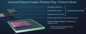
Teramount’s approach couples the fibre to the silicon photonics chip using two components: a photonic plug and a photonic bump.
The photonic plug holds the fibres and couples them to the silicon photonics chip via the photonic bump, a component made during the silicon photonics wafer processing. The photonic bump consists of two elements: a wideband deflector and a lens mirror for beam expansion. Expanding the light beam enables much larger assembly tolerances: +/- 30 microns. And across this 60-micron window, only half a dB is lost in misalignment tolerances.
The resulting wafer-level manufacturing may be more complicated, says Taha, but the benefit is relaxed tolerances in the assembly, wide-band surface coupling, and when testing the wafer and the die.
The photonic bump-and-plug combination also enable detachable optics for co-packaged optics designs. This benefits manufacturing and is wanted for co-packaged optics.
Teraverse and Teraverse-XD
There is a clear demarcation between the optics and the switch chip when using pluggables in the data centre. In contrast, co-packaged optics is a system with the optics embedded alongside the chip. A vendor may work with multiple companies to make co-packaged optics, but one product results, with the chip and optical engined co-packaged.
Teramount’s Teraverse solution, using the plug-and-bump combination, brings pluggability to co-packaged optics. The fibres can be attached and detached from the optical engines. “It’s very important to keep that level of pluggability for co-packaged optics,” says Taha.
The approach also benefits manufacturing yield and testing. Separating the fibres from the package protects the fibres during reflow soldering. “Ideally, you want the fibre connected at the last stage and still maintain high level of testability during the packaging process,” says Taha.
Detachable fibre also brings serviceability to co-packaged optics, benefitting for data centre operators.
Teraverse, Teramount’s detachable fiber-to-chip interface, supports single-mode fiber with 125-micron diameter at a 127-micron pitch separation.

Teraverse-XD, announced for OFC, is a follow-on that doubles the fibre density to achieve a near 64-micron pitch. Here, fibres are placed on top of each other, scaling in the Z-dimension. The approach is like how rods or pipes are stored, with the second row of fibres staggered, sitting in the valleys between adjacent fibers in the lower row.
Two rows of photonic bumps are used to couple the light to each row of fibres (see image above). “It’s very important to keep the same real-estate but to have twice the number of fibres,” says Taha.
Future scaling is possible by adding more rows of fibres or by adopting fibres with a smaller pitch.
Teramount’s technology also supports both edge coupling and surface coupling. “We are agnostic,” says Taha. If a co-packaged optics or optical engine vendor wants to use side coupling, it can use the bump-and-plug combination. The bump deflects the beam upwards to the plug packaging which takes the fibres and sends them out horizontally. “We are converting edge coupling to wideband surface coupling,” says Taha. “You don’t need to sacrifice bandwidth to do surface coupling.”
If the vendor wishes to use a grating coupler, Teramount’s bump-and-plug supports that, too, enabling detachable fibering. But here, only the bump’s expanding mirror is used. “For the wideband surface coupling cased, the bump uses two components: the deflector and the expanding mirror,” says Taha.
Both cases are supported by what Teramount refers to as its Universal Photonic Coupler, shown.
Market expectations
Despite being discussed for over a decade, Taha is not surprised that data centre operators have yet to adopt co-packaged optics.
He points out that hyperscalers only want to use co-packaged optics for Ethernet switches once the technology is more mature. They can also keep using a proven alternative: pluggable modules, that continue to advance.
“Hyperscalers are not against the technology, but it is not mature enough,” says Taha. Hyperscalers and systems vendors also want an established supply chain and not proprietary solutions.
To date, Broadcom’s first co-packaged optics switch solution at 25.6-terabit was adopted by Tencent. Broadcom has announced for OFC that it is now delivering its latest 51.2-terabit Bailly co-packaged optics design, backed by ByteDance.
“AI is a different story,” says Taha. “This is the tipping point for a leading vendor to start taking seriously co-packaged optics.”
The advantage of co-packaged optics here is that it accommodates the reach – radix -as well as power savings and improved latency.
Taha expects initial volumes of co-packaged optics sales in 2026.

Packaging silicon photonics using passive alignment
- An Israeli start-up is tackling a key packaging challenge for silicon photonics
Teramount has developed a way to simplify the packaging of silicon photonics chips. Instead of using active alignment whereby an external laser is required to carefully align a fibre to the optical die, the Israeli start-up has developed a technology that allows passive alignment.
 Hesham Taha“If we want silicon photonics to ramp up to volume, it has to meet CMOS standards both in terms of fabrication and packaging,” says Hesham Taha, Teramount's CEO.
Taha worked at a company developing atomic force microscopy systems before co-founding Teramount. "We got to know of the problem of injecting light into a waveguide and were surprised that the industry was still using active alignment," he says.
This spurred Taha and a colleague to develop optical solutions to match a single-mode fibre core to an optical waveguide, and they founded Teramount in Jerusalem in 2013. "We started real activity at the beginning of 2015 after getting funding," says Taha.
Existing silicon photonics companies either develop their own customised active alignment equipment or outsource the activity to a third party. "If we solve one of the bottlenecks of silicon photonics in terms of packaging, silicon photonics will be more and more adopted," says Taha.
If we want silicon photonics to ramp up to volume, it has to meet CMOS standards both in terms of fabrication and packaging
The design
Teramount's solution includes two elements: a PhotonicsPlug that is flip-chipped onto the silicon photonics die while still part of a wafer, and a 'bump', a design element added on the silicon photonics chip next to the optical waveguide. "Our solution, which we will be selling, is the PhotonicsPlug and we do require them [the designers] to add one element [the bump] to their silicon photonics chip," says Taha.
The main PhotonicsPlug component is a silicon die comprising optics that manipulates the beam using self-aligning optics and focusses it onto the silicon photonics chip via a glass spacer. Teramount’s die also has V-grooves to interface the single-mode ribbon fibre. Teramount says its die is made using an inexpensive mature CMOS process due to the relatively large feature sizes of the optical elements.
The second design element - the bump - is added next to the silicon photonics chip's grating coupler. The grating coupler is one of two techniques used in the industry to interface a fibre to the waveguide, the other being edge coupling.
“We want to place it [the bump] next to the waveguide so that the optics of the PhotonicPlug works in conjunction with it so that it brings the beam to the waveguide with a large tolerance,” says Taha. The bump is accurately placed on the chip using standard lithography techniques.
The resulting tolerance with which the die can be attached to the silicon photonics wafer is up to ± 20 microns in each of the three dimensions such that standard flip-chip machines can attach the PhotonicsPlug to the wafer.
“Flip-chip machines today work with a tolerance of ± 6 microns and can do 1,500 assemblies per hour,” says Taha.
"This is the main philosophy we are bringing here," he says. "Instead of the accurate placement of the fibre next to the grating coupler which requires active alignment, we want to replace that with a cheaper alignment technique that has much better accuracy at the wafer level," says Taha.
Status
Teramount has already shown working devices using the technology. In addition, Teramount is working with several partners and has demonstrated its technology with their silicon photonics chip designs. "With these partners we are doing the integration and qualifying the performance of the device," says Taha. "We will finalise at least two of these partnerships within a few months."
The start-up is also working to enable volume manufacturing by bringing its technology to industrial fabrication plants. This will be completed in the next few months.
Being a small start-up, the company is focussed on developing the grating coupler solution but it has already started work on an edge-coupling technique to a device’s waveguides. Edge coupling is suited to wavelength-division multiplexing (WDM) silicon photonics chips. That is because grating couplers are wavelength-dependent while edge coupling supports a broader range of wavelengths.