
Turning to optical I/O to open up computing pinch points

Getting data in and out of chips used for modern computing has become a key challenge for designers.
A chip may talk to a neighbouring device in the same platform or to a chip across the data centre.
The sheer quantity of data and the reaches involved – tens or hundreds of meters – is why the industry is turning to optical for a chip’s input-output (I/O).
It is this technology transition that excites Ayar Labs.
The US start-up showcased its latest TeraPHY optical I/O chiplet operating at 1 terabit-per-second (Tbps) during the OFC virtual conference and exhibition held in June.
Evolutionary and revolutionary change
Ayar Labs says two developments are driving optical I/O.
One is the exponential growth in the capacity of Ethernet switch chips used in the data centre. The emergence of 25.6-terabit and soon 51.2-terabit Ethernet switches continue to drive technologies and standards.
This, says Hugo Saleh, vice president of business development and marketing, and recently appointed as the managing director of Ayar Labs’ new UK subsidiary, is an example of evolutionary change.
But artificial intelligence (AI) and high-performance computing have networking needs independent of the Ethernet specification.
“Ethernet is here to stay,” says Saleh. “But we think there is a new class of communications that is required to drive these advanced applications that need low latency and low power.”
Manufacturing processes
Ayar Labs’ TeraPHY chiplet is manufactured using GlobalFoundries’ 45nm RF Silicon on Insulator (45RFSOI) process. But Ayar Labs is also developing TeraPHY silicon using GlobalFoundries’ emerging 45nm CMOS-silicon photonics CLO process (45CLO).
The 45RFSOI process is being used because Ayar Labs is already supplying TeraPHY devices to customers. “They have been going out quite some time,” says Saleh.
But the start-up’s volume production of its chiplets will use GlobalFoundries’ 45CLO silicon photonics process. Version 1.0 of the process design kit (PDK) is expected in early 2022, leading to qualified TeraPHY parts based on the process.
One notable difference between the two processes is that 45RFSOI uses a vertical grating coupler to connect the fibre to the chiplet which requires active alignment. The 45CLO process uses a v-groove structure such that passive alignment can be used, simplifying and speeding up the fibre attachment.
“With high-volume manufacturing – millions and even tens of millions of parts – things like time-in-factory make a big difference,” says Saleh. Every second spent adds cost such that the faster the processes, the more cost-effective and scalable the manufacturing becomes.
Terabit TeraPHY
The TeraPHY chiplet demonstrated during OFC uses eight optical transceivers. Each transceiver comprises eight wavelength-division multiplexed (WDM) channels, each supporting 16 gigabit-per-second (Gbps) of data. The result is a total optical I/O bandwidth of 1.024Tbps operating in each direction (duplex link).
“The demonstration is at 16Gbps and we are going to be driving up to 25Gbps and 32Gbps next,” says Saleh.
The chiplet’s electrical I/O is slower and wider: 16 interfaces, each with 80, 2Gbps channels implementing Intel’s Advanced Interface Bus (AIB) technology.
Last December, Ayar Labs showcased advanced parts using the CLO process. The design was a direct-drive part – a prototype of a future-generation product, not the one demonstrated for OFC.
“The direct-drive part has a serial analogue interface that could come from the host ASIC directly into the ring resonators and modulate them whereas the part we have today is the productised version of an AIB interface with all the macros and all the bandwidth enabled,” says Saleh.
Ayar Labs also demonstrated its 8-laser light source, dubbed SuperNova, that drives the chiplet’s optics.
The eight distributed feedback (DFB) lasers are mixed using a planar lightwave circuit to produce eight channels, each comprising eight frequencies of light.
Saleh compares the SuperNova to a centralised power supply in a server that power pools of CPUs and memory. “The SuperNova mimics that,” he says. “One SuperNova or a 1 rack-unit box of 16 SuperNovas distributing continuous-wave light just like distributed voltage [in a server].”
The current 64-channel SuperNova powers a single TeraPHY but future versions will be able to supply light to two or more.
Ayar Labs is using Macom as its volume supplier of DFB lasers.
Significance
Ayar Labs believes the 1-terabit chip-to-chip WDM link is an industry first.
The demo also highlights how the company is getting closer to a design that can be run in the field. The silicon was made less than a month before the demonstration and was assembled quickly. “It was not behind glass and was operating at room temperature,” says Saleh. “It’s not a lab setting but a production setting.”
The same applies to the SuperNova. The light source is compliant with the Continuous-Wave Wavelength Division Multiplexing (CW-WDM) Multi-Source Agreement (MSA) Group that released its first specification revision to coincide with OFC. The CW-WDM MSA Group has developed a specification for 8, 16, and 32-wavelength optical sources.
The CW-WDM MSA promoter and observer members include all the key laser makers as well as the leading ASIC vendors. “We hope to establish an ecosystem on the laser side but also on the optics,” says Saleh.
“Fundamentally, there is a change at the physical (PHY) level that is required to open up these bottlenecks,” says Saleh. “The CW-WDM MSA is key to doing that; without the MSA you will not get that standardisation.”
Saleh also points to the TeraPHY’s optical I/O’s low power consumption which for each link equates to 5pJ/bit. This is about a tenth of the power consumed by electrical I/O especially when retimers are used. Equally, the reach is up to 2km not tens of centimetres associated with electrical links.
Chiplet demand
At OFC, Arista Networks outlined how pluggable optics will be able to address 102.4 terabit Ethernet switches while Microsoft said it expects to deploy co-packaged optics by the second half of 2024.
Nvidia also discussed how it clusters its graphics processing units (GPUs) that are used for AI applications. However, when a GPU from one cluster needs to talk to a GPU in another cluster, a performance hit occurs.
Nvidia is looking for the optical industry to develop interfaces that will enable its GPU systems to scale while appearing as one tightly coupled cluster. This will require low latency links. Instead of microseconds and milliseconds depending on the number of hops, optical I/O reduces the latency to tens of nanoseconds.
“We spec our chiplet as sub-5ns plus the time of flight which is about 5ns per meter,” says Saleh. Accordingly, the transit time between two GPUs 1m apart is 15ns.
Ayar Labs says that after many conversations with switch vendors and cloud players, the consensus is that Ethernet switches will have to adopt co-packaged optics. There will be different introductory points for the technology but the industry direction is clear.
“You are going to see co-packaged optics for Ethernet by 2024 but you should see the first AI fabric system with co-packaged I/O in 2022,” says Saleh.
Intel published a paper at OFC involving its Stratix 10 FPGA using five Ayar Labs’ chiplets, each one operating at 1.6 terabits (each optical channel operating at 25Gbps, not 16Gbps). The resulting FPGA has an optical I/O capacity of 8Tbps, the design part of the US DARPA PIPES (Photonics in the Package for Extreme Scalability) project.
“A key point of the paper is that Intel is yielding functional units,” says Saleh. The paper also highlighted the packaging and assembly achievements and the custom cooling used.
Intel Capital is a strategic investor in Ayar Labs, as is GlobalFoundries, Lockheed Martin Ventures, and Applied Materials.
Intel details its 800-gigabit DR8 optical module

The company earmarks 2023 for its first co-packaged optics product
Intel is sampling an 800-gigabit DR8 in an OSFP pluggable optical module, as announced at the recent OFC virtual conference and show.
“It is the first time we have done a pluggable module with 100-gigabit electrical serdes [serialisers/ deserialisers],” says Robert Blum, Intel’s senior director, marketing and new business. “The transition for the industry to 100-gigabit serdes is a big step.”
The 800-gigabit DR8 module has eight electrical 100-gigabit interfaces and eight single-mode 100-gigabit optical channels in each transmission direction.
Intel demonstrated a prototype 12.8-terabit co-packaged optics design
The attraction of the single-module DR8 design, says Blum, is that it effectively comprises two 400-gigabit DR4 modules. “The optical interface allows you the flexibility that you can break it out into 400-gigabit DR4,” says Blum. “You can also do single 100-gigabit breakouts or you can do 800-gigabit-to-800-gigabit traffic.”
Intel expects volume production of the DR8 in early 2022. Developing a DR8 in a QSFP-DD800 form factor will depend on customer demand, says Blum.
Intel will follow the 800-gigabit DR8 module with a dual 400G FR4, expected later in 2022. The company is also developing a 400-gigabit FR4 module that is expected then.
Meanwhile, Intel is ramping its 200-gigabit FR4 and 400-gigabit DR4 modules.
51.2-terabit co-packaged optics
Intel demonstrated a prototype 12.8-terabit co-packaged optics design, where the optics is integrated alongside its Tofino 2 Ethernet switch chip, at last year’s OFC event.
The company says its first co-packaged optics design will be for 51.2-terabit switches and is scheduled in late 2023. “We see smaller-scale deployments at 51.2 terabits,” says Blum.
Moving the industry from pluggable optical modules to co-packaged optics is a big shift, says Intel. The technology brings clear system benefits such as 30 per cent power savings and lower cost but these must be balanced against the established benefits of using pluggable modules and the need to create industry partnerships for the production of co-packaged optics.
The emergence of 800-gigabit client-side pluggable modules such as Intel’s also means a lesser urgency for co-packaged optics. “You have something that works even if it is more expensive,” says Blum.
Thirty-two 800-gigabit modules can serve a 25.6-terabit switch in a one rack unit (1RU) platform.
However, for Intel, the crossover point occurs once 102.4-terabit switch chips and 200-gigabit electrical interfaces emerge.
“We see co-packaged optics as ubiquitous; we think pluggables will no longer make sense at that point,” says Blum.
FPGA-based optical input-output
Intel published a paper at OFC 2021 highlighting its latest work a part of the U.S. DARPA PIPES programme.
The paper describes a co-packaged optics design that adds 8 terabits of optical input-output (I/0) to its Stratix 10 FPGA. The design uses Ayar Labs’ TeraPHY chiplet for the optical I/O.
The concept is to use optical I/O to connect compute nodes – in this case, FPGAs – that may be 10s or 100s of meters apart.
Intel detailed its first Stratix 10 with co-packaged optical I/O two years ago.
The latest multi-chip package also uses a Stratix 10 FPGA with Intel’s Advanced Interface Bus (AIB), a parallel electrical interface technology, as well as the Embedded Multi-die Interconnect Bridge (EMIB) technology which supports the dense I/O needed to interface the FPGA to the TeraPHY chiplet. The latest design integrates five TeraPHYs compared to the original one that used two. Each chiplet offers 1.6 terabits of capacity such that the FPGA-based co-package has 8 terabits of I/O in total.
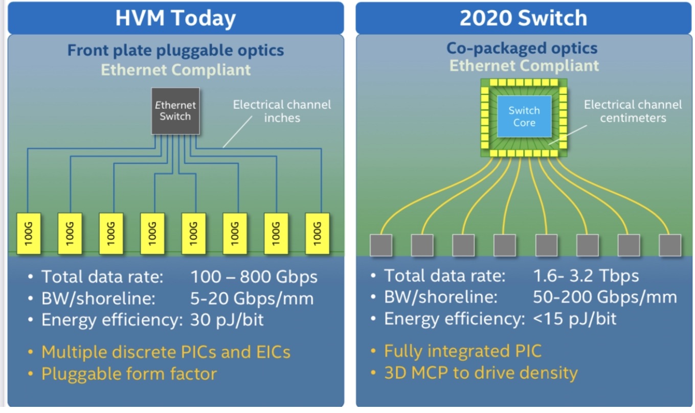
Optically enabling Ethernet silicon or an FPGA is part of the industry’s vision to bring optics close to the silicon. Other devices include CPUs and GPUs and machine-learning devices used in computing clusters that require high-density interconnect (see diagram below).
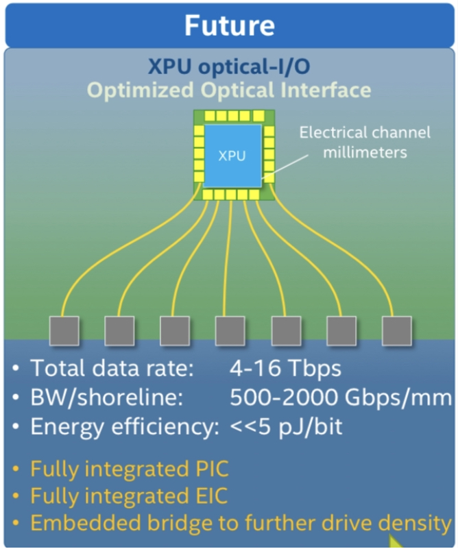
“It is happening first with some of the highest bandwidth Ethernet switches but it is needed with other processors as well,” says Blum.
The Intel OFC 2021 paper concludes that co-packaged optics is inevitable.
Milestones, LiDAR and sensing
Intel has shipped a total of over 5 million 100-gigabit optical modules, generating over $1 billion of revenues.
Blum also mentioned Intel’s Mobileye unit which in January announced its LiDAR-on-a-chip design for autonomous vehicles.
“We have more than 6,000 individual components on this LiDAR photonic integrated circuit,” says Blum. The count includes building blocks such as waveguides, taps, and couplers.
“We have this mature [silicon photonics] platform and we are looking at where else it can be applied,” says Blum.
LiDAR is one obvious example: the chip has dozens of coherent receivers on a chip and dozens of semiconductor optical amplifiers that boost the output power into free space. “You really need to integrate the different functionalities for it to make sense,” says Blum.
Intel is also open to partnering with companies developing biosensors for healthcare and for other sensing applications.
Certain sensors use spectroscopy and Intel can provide a multi-wavelength optical source on a chip as well as ring-resonator technology.
“We are not yet at a point where we are a foundry and people can come but we could have a collaboration where they have an idea and we make it for them,” says Blum.