Optical is being added as a second physical medium to the PCI Express (PCIe) data transfer protocol.
PCI Express is an electrical standard, but now the Peripheral Component Interconnect Special Interest Group (PCI-SIG) has created a working group to standardise PCIe’s delivery optically.
PCI-SIG is already developing copper cabling specifications for the PCI Express 5.0 and 6.0 standards.
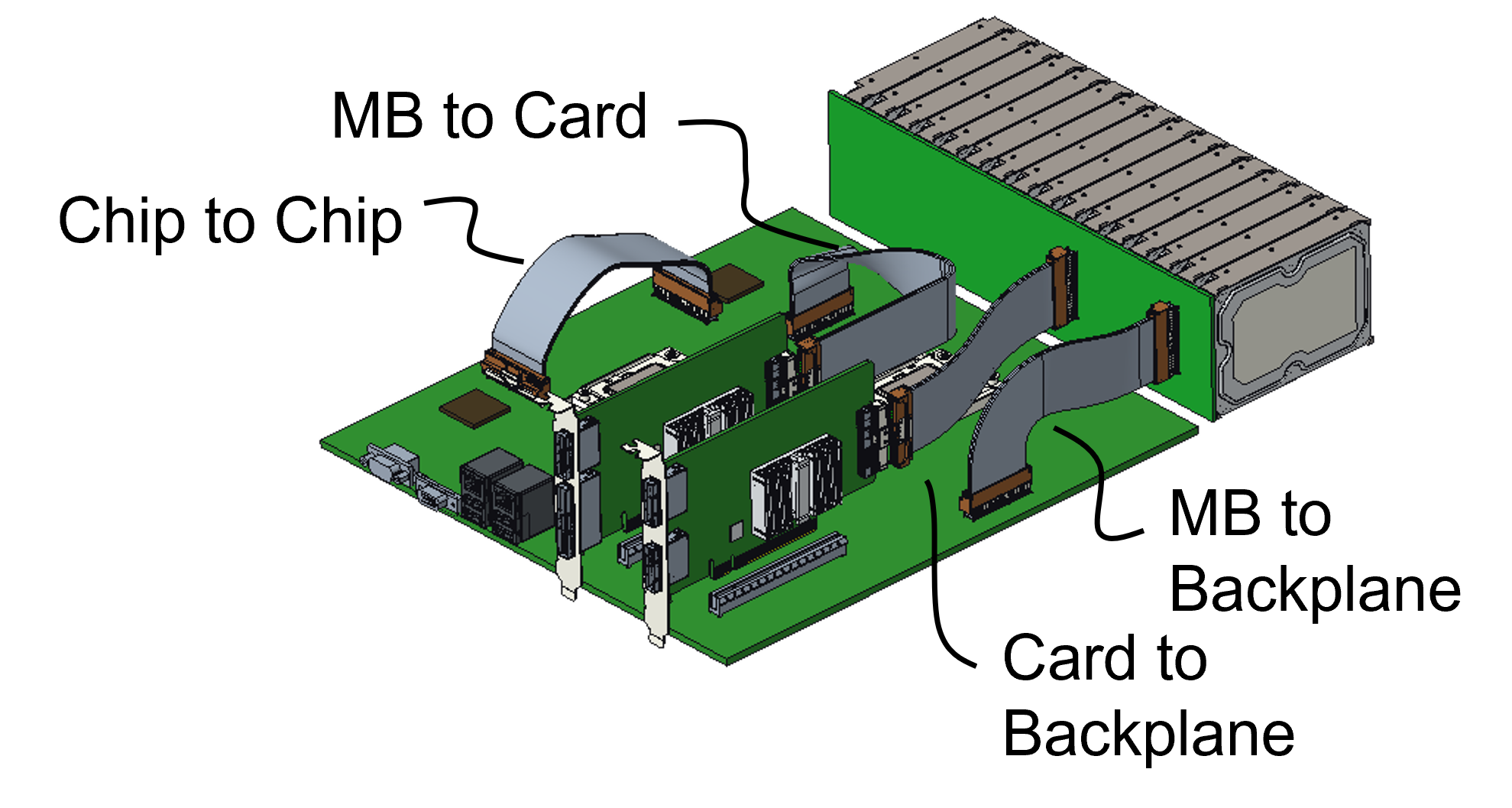
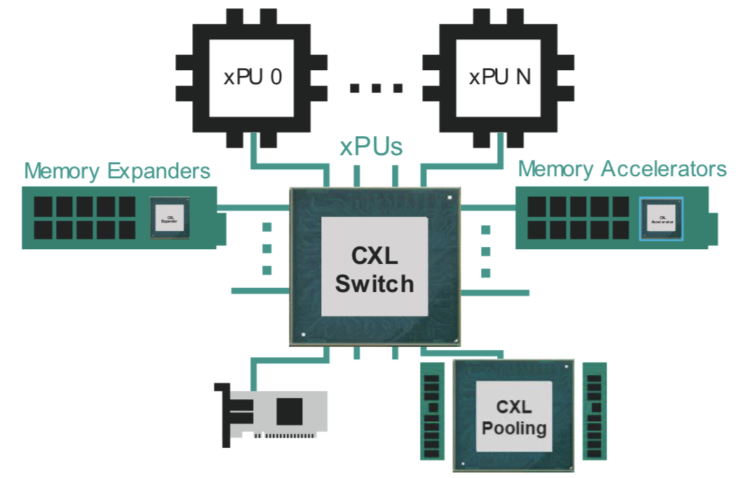
Since each generation of PCIe doubles the data transfer rate, PCI-SIG member companies want copper cabling to help with the design of high-speed PCIe interconnects on a printed circuit board (PCB), between PCBs, and between racks (see diagram).
“We’ve seen a lot of interest over recent months for an optical cable that will support PCI Express,” says Al Yanes, PCI-SIG president and chairperson.
He cites the trends of the decreasing cost and size of optics and how silicon photonics enables the adding of optics alongside ASICs.
“We have formed a workgroup to deliver an optical cable,” says Yanes. “There are many applications, but one is a longer-distance reach for PCI Express.”
“It is a void in the market [the lack of optical support for PCIe], and it needs to be filled,” says Bill Koss, CEO of Drut Technologies. “These efforts tend to take longer than estimated, so better to start sooner.”
The data centre is going photonic, says Koss, so there is a need for such working standards as photonics get closer to processors.
The PCIe protocol
PCIe is used widely across many industries.
In the data centre, PCIe is used by general-purpose microprocessors and accelerator chips, such as FPGAs, graphics processing units and AI hardware, to connect to storage and network interface cards.
The PCIe bus uses point-to-point communications based on a simple duplex scheme – serial transmissions in both directions which is referred to as a lane.
The bus can be bundled in various lane configurations – x1, x2, x4, x8, x12, x16 and x32 – with x4, x8 and x16 the configurations most used.
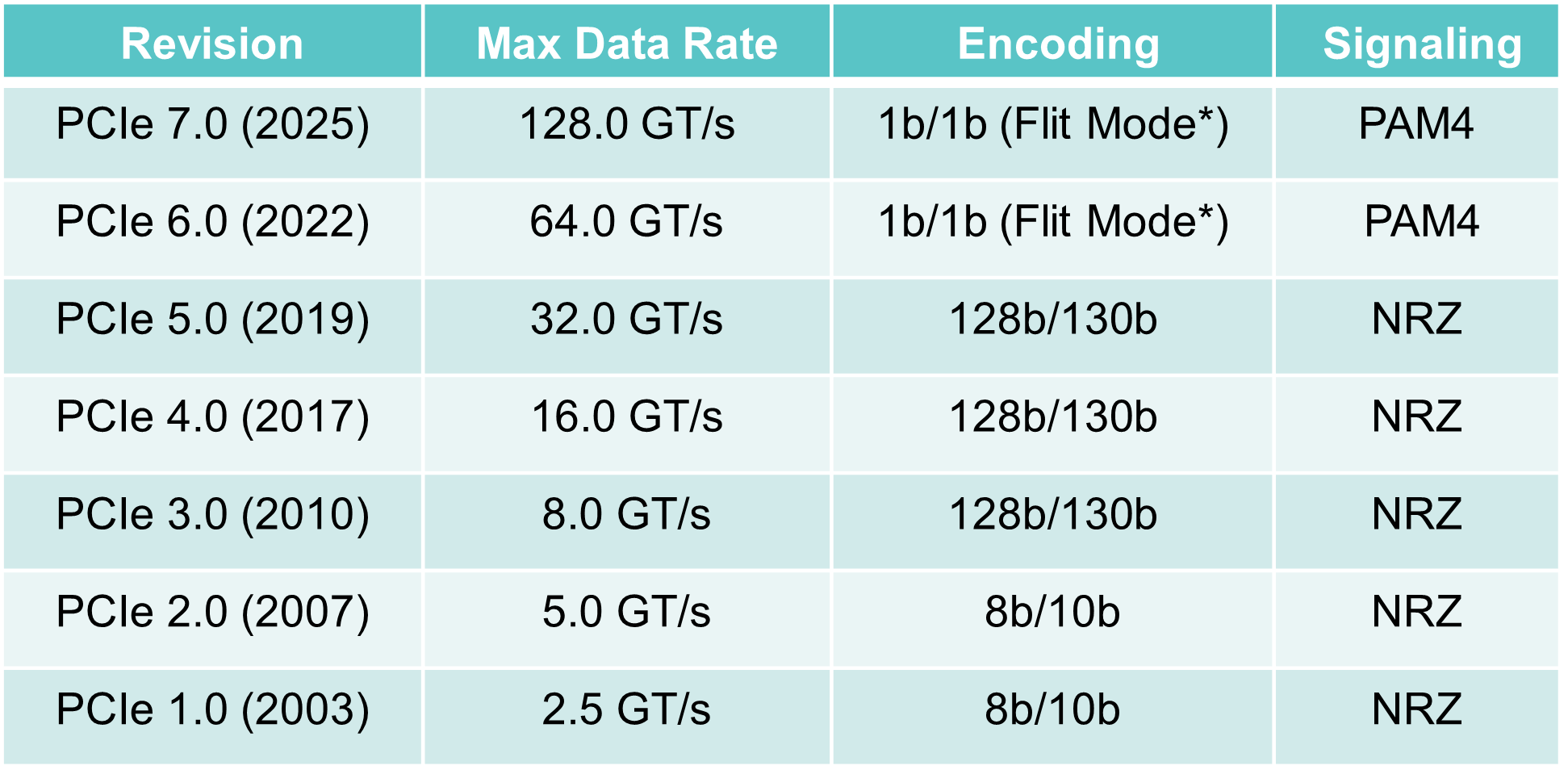
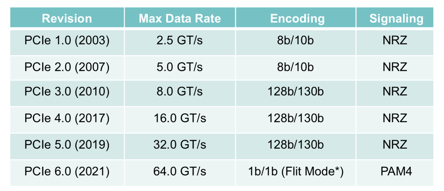
The first two PCIe versions, 1.0 and 2.0, delivered 2.5 and 5 giga transfers-per-second (GT/s) per lane per direction, respectively.
A transfer refers to an encoded bit. The first two PCIe versions use an 8b/10b encoding scheme such that for every ten-bit payload sent, 8 bits are data. This is why the data transfer rates per lane per direction are 2Gbps and 4Gbps (250 and 500 gigabytes per second), respectively.
With PCIe 3.0, the decision was made to increase the transfer rate to 8GT/s per lane, which assumed that no equalisation would be needed to counter inter-symbol interference at that speed. However, equalisation was required, which explains why PCIe 3.0 adopted 8GT/s and not 10GT/s.
Source: PCI-SIG
Another PCIe 3.0 decision was to move to a 128b/130b scheme to reduce the encoding overhead from 20 per cent to over 1 per cent. Now the transfer and bit rates are almost equal from the PCIe 3.0 standard onwards.
PCIe 4.0 doubles the transfer rate from 8GT/s to 16GT/s, while PCIe 5.0 is 32GT/s per lane per direction.
Since then, PCIe 6.0 has been specified, supporting 64GT/s per lane per direction. PCIe 6.0 is the first standard for 4-level pulse amplitude modulation (PAM4) signalling.
Now the PCIe 7.0 specification work is at version 0.3. PCIe 7.0 uses PAM-4 to deliver 128GT/s per lane per direction. The standard is expected to be completed in 2025, with industry adoption in 2027.
Optical cabling for PCIe
The PCI Express 5.0 and 6.0 copper cabling specifications are expected by the year-end. The expected distance using copper cabling and retimers is 5-6m.
The reach of an optical PCIe standard will ‘go a lot further’ than that, but how far is to be determined.
Yanes says optical cables for PCIe will also save space: “An optical cable is not as bulky nor as thick as a copper cable.”
Whether the optical specification work will support all versions of PCIe is to be determined.
“There’s some interest to support them all; the copper solution supports all the negotiations,” says Yanes. “It’s something that needs to be discussed, but, for sure, it will be the higher speeds.”
The working group will decide what optical options to specify. “We know that there are some basic things that we need to do to PCI Express technology to make it support optics,” says Yanes.
The working group aims to make the specification work generic enough that it is ‘optical friendly’.
“There are many optical techniques in the industry, and there is discussion as to which of these optical techniques is going to be the winner in terms of usage,” says Yanes. “We want our changes to make PCI Express independent of that discussion.”
The organisation will make the required changes to the base specification of PCIe to suit optical transmission while identifying which optical solutions to address and build.
PCI-SIG will use the same Flit Mode and the same link training, for example, while the potential specification enhancements include coordinating speed transitions to match the optics, making side-band signals in-band, and making the specification more power-efficient given the extended reach.
Pluggable optical modules, active optical cables, on-board optics, co-packaged optics and optical input-output are all optical solutions being considered.
An optical solution for PCIe will also benefit technologies such as Compute Express Link (CXL) and the Non-Volatile Memory Express (NVMe) protocols implemented over PCIe. CXL, as it is adopted more broadly, will likely drive new uses that will need such technology.
The PCIe optical working group will complete the specifications in 12-18 months. Yanes says a quicker working solution may be offered before then.
Enfabrica’s accelerated compute fabric chip is designed to scale computing clusters comprising CPUs and specialist accelerator chips.
The chip uses memory disaggregation and high-bandwidth networking for accelerator-based servers tackling artificial intelligence (AI) tasks.
For over a decade, cloud players have packed their data centres with x86-based CPU servers linked using tiers of Ethernet switches.
“The reason why Ethernet networking has been at the core of the infrastructure is that it is incredibly resilient,” says Rochan Sankar, CEO and co-founder of Enfabrica.
But the rise of AI and machine learning is causing the traditional architecture to change.
What is required is a mix of processors: CPUs and accelerators. Accelerators are specialist processors such as graphics processing units (GPUs), programmable logic (FPGAs), and custom ASICs developed by the hyperscalers.
It is the accelerator chips, not the CPUs, that do the bulk of the processing. Accelerators also require vast data, creating challenging input-output (I/O) and memory requirements.
At Optica’s Executive Forum event, held alongside the OFC show in March, Ryohei Urata, director and principal engineer at Google, mentioned how Google uses two computing pods – comprising 6,000 TPU accelerators – to run its large language models.
A key concern for Google is scaling such clusters while ensuring their reliability and availability. It is critical that the system is available when running a large language model, says Urata,
“As an engineer, when you’re putting stuff down, at least when you’re first start to put it together, you think, okay, this is going to work perfectly,” says Urata. “This is a perfect design, you don’t factor in failing gracefully, so that’s a key lesson.”
Google’s concern highlights that accelerator-based clusters lack the reliability of data centre server-Ethernet networks.
Accelerated compute fabric
Start-up Enfabrica has developed a chip, dubbed the accelerated compute fabric, to scale computing clusters.
“The focus of Enfabrica is on how networking and fabric technologies have to evolve in the age of AI-driven computing,” says Sankar.
AI models are growing between 8x to 275x annually, placing enormous demands on a data centre’s computing and memory resources.
“Two hundred and seventy-five times are of the order of what the large language models are increasing by, 8x is more other models including [machine] vision; recommender models are somewhere in between,” says Sankar.
Another AI hardware driver is growing end-user demand; ChatGPT gained 100 million users in the first months after its launch.
Meeting demand involves cascading more accelerators but the I/O bandwidth connected to the compute is lagging. Moreover, that gap is growing.
Sankar includes memory bandwidth as part of the I/O issue and segments I/O scaling into two: connecting CPUs, GPUs, accelerators and memory in the server, and the I/O scaling over the network.
A computing architecture for AI must accommodate greater CPUs and accelerators yet tackle the I/O bottleneck.
“To scale, it requires disaggregation; otherwise, it becomes unsustainable and expensive, or it can’t scale enough to meet processing demands,” says Sankar
“Memory disaggregation represents the last step in server disaggregation, following storage and networking,” says Bob Wheeler, principal analyst at Wheeler’s Network.
Memory expansion through disaggregation has become more urgent as GPUs access larger memories for AI training, particularly for large language modules like ChatGPT, says Wheeler.
Rethinking data connectivity
In the data centre, servers in a rack are linked using a top-of-rack switch. The top-of-rack switch also connects to the higher-capacity leaf-spine Ethernet switching layers to link servers across the data centre.
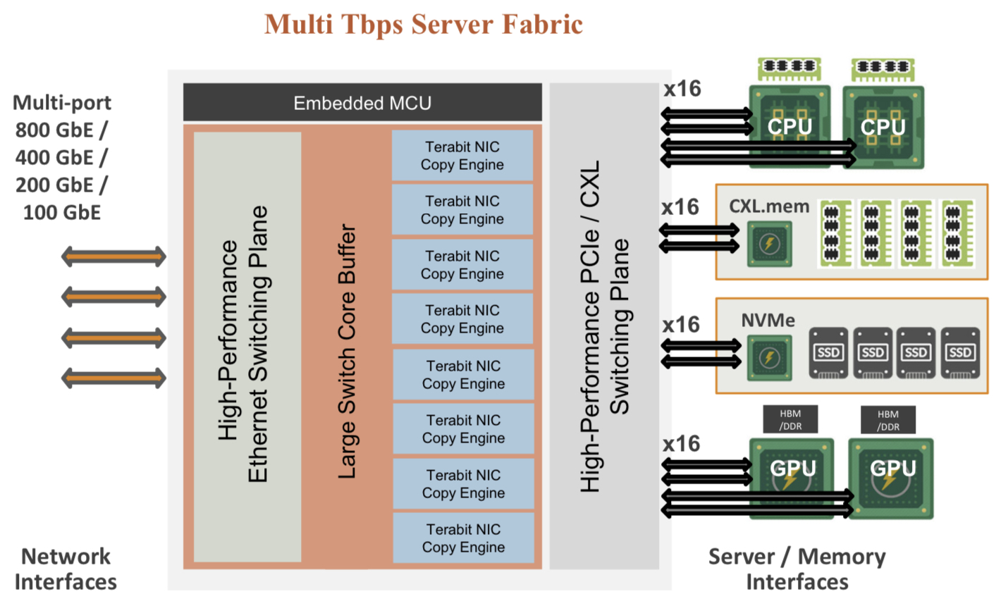
Enfabrica proposes that the higher capacity Ethernet switch leaf layer talks directly to its accelerated compute fabric chip, removing the top-of-rack switch.
Source: Enfabrica
In turn, the accelerated compute fabric uses memory mapping to connect CPUs, accelerators, disaggregated memory pools using CXL, and disaggregated storage (see diagram above).
The memory can be a CPU’s DDR DRAM, a GPU’s high-bandwidth memory (HBM), a disaggregated compute express link (CXL) memory array, or storage.
“It [the accelerated compute fabric] connects to them over standard memory-mapped interfaces such as PCI Express (PCIe) or CXL,” says Sankar.
The functional blocks and interfaces of the accelerate compute fabric architecture. Source: Enfabrica
The chip uses ‘copy engines’ to move data to and from any processing element’s native memory. And by performing memory transfers in parallel, the chip is doing what until now has required PCIe switches, network interface cards (NICs), and top-of-rack switches.
The accelerated compute fabric also has 800-gigabit network interfaces so that, overall, the chip has terabits of bandwidth to move data across the network.
“CXL provides a standard way to decouple memories from CPUs, enabling DRAM disaggregation,” says Wheeler. “Enfabrica’s copy engines connect the GPUs to the pool of CXL memory. The network side, using RDMA (remote direct memory access), enables scaling beyond the limits of CXL.”
Sankar stresses that the accelerated compute fabric is much more than an integration exercise using an advanced 5nm CMOS process.
“If you were to integrate eight NICs, four PCIe switches and a top-of-rack switch, it would not fit into a single die,” says Sankar.
As for software, Enfabrica has designed its solution to fit in with how GPUs, CPUs and memory move data.
Significance
Sankar says the accelerated compute fabric IC will shorten job completion time because the scheduler is finer-grained and the chip can steer I/O to resources as required.
Computing clusters will also become larger using the IC’s high-density networking and CXL.
Wheeler says that CXL 3.x fabrics could provide the same capabilities as the accelerated compute fabric, but such advanced features won’t be available for years.
“History suggests some optional features included in the specifications will never gain adoption,” says Wheeler.
“The CXL/PCIe side of the [accelerated compute fabric] chip enables memory disaggregation without relying on CXL 3.x features that aren’t available, whereas the RNIC (RDMA NIC) side allows scaling to very large systems for workloads that can tolerate additional latency,” says Wheeler.
System benefits
Sankar cites two GPU platforms – one proprietary and one an open system – to highlight its chip benefits. The platforms are Nvidia’s DGX-H100 box and the open-design Grand Teton announced by Meta.
“The DGX has become a sort of fundamental commodity or a unit of AI computing,” says Shankar.
The DGX uses eight H100 GPUs, CPUs (typically two), I/O devices that link the GPUs using NVlink, and Infiniband for networking. The Meta platform has a similar specification but uses Ethernet.
Both systems have eight 400-gigabit interfaces. “That is 3.2 terabits coming out of the appliance, and inside the device, there is 3.2 terabit connected to a bunch of compute resources,” says Sankar.
The Meta platform includes layers of PCIe switches, and Open Compute Project (OCP 3.0) NICs running at 200 gigabits, going to 400 gigabits in the next generation.
The Grand Teton platform also uses eight NICs, four PCIe switches, and likely a top-of-rack switch to connect multiple systems.
Enfabrica’s vision is to enable a similarly composable [GPU] system. However, instead of eight NICs, four PCIe switches and the external top-of-rack switch, only three devices would be needed: two Enfabrica accelerated compute fabric chips and a control processor.
Enfabrica says the design would halve the power compared to the existing NICs, PCIe switches and the top-of-rack switch. “That represents 10 per cent of the rack’s power,” says Sankar.
And low-latency memory could be added to the space saved by using three chips instead of 12. Then, the eight GPUs would have tens of terabytes of memory to share whereas now each GPU has 80 gigabytes of HBM.
What next?
Enfabrica is unveiling the architecture first, and will detail its product later this year.
It is key to unveil the accelerated compute fabric concept now given how AI architectures are still nascent, says Sankar.
But to succeed, the start-up must win a sizeable data-centre customer such as a hyperscaler, says Wheeler: “That means there’s a very short list of customers, and winning one is paramount.”
The supplier must deliver high volumes from the start and guarantee supply continuity, and may also have to provide the source code to ensure that a customer can maintain the product under any circumstances.
“These are high hurdles, but Innovium proved it can be done and was rewarded with an exit at a valuation of greater than $1 billion,” says Wheeler.
In a wide-ranging interview, Noam Mizrahi (pictured), executive vice president and corporate chief technology officer (CTO) at Marvell, discusses the many technologies needed to succeed in the data centre. He also discusses a CTO’s role and the importance of his focussed thinking ritual.
Noam Mizrahi has found his calling.
“I’m inspired by technology,” he says. “Every time I see an elegant technical solution – and it can be very simple – it makes me smile.”
Marvell hosts an innovation contest, and at one event, Mizrahi mentioned this to participants. “So they issued stickers saying, ‘I made Noam smile’,” he says.
Marvell’s broad portfolio of products spans high-end processors, automotive Ethernet, storage, and optical modules.
“This technology richness means that every day I come to work, I feel I learn something new,” he says.
Chip design
The interview with Mizrahi occurred before the passing away on March 24th of Gordon Moore, aged 94, who co-founded Intel.
In his article published in Electronics in 1965, Moore observed how chip transistor count doubled roughly yearly, what became known as Moore’s law.
The law has driven the semiconductor industry for decades and, like all exponential trends, is reaching its limit.
Since Marvell’s business is infrastructure ICs, it is experiencing the law’s demise first hand.
While the core definition of Moore’s law is ending, technology and process advancement are still enabling the cramming of more transistors on a die, says Mizrahi. However, greater processing performance and lower power consumption are occurring at a different pace and cost structure.
It is now very costly to make chips using the latest 5nm and 3nm CMOS process nodes.
The cost is not just the chip mask (reticle) but also such aspects as intellectual property (IP), architecture, design verification, electronics design automation (EDA) tools, and design validation.
Getting to the first product using 5nm CMOS can cost as high as $450 million, while for 3nm, the estimate is $600 million.
Also, development flow takes longer due to the complexity involved and will cause a redefinition of what is meant by a ‘current generation’ of a chip, says Mizrahi.
Design reuse is also increasingly required; not just reusing IP but the validation process in order to speed up a chip’s introduction.
In turn, designers must be innovative since processing performance and lower power consumption are harder to achieve.
Areas include package design optimisation, chip input-output (I/O), and the software to claw back processing performance that previously came from using the latest CMOS process.
IC designers will also be forced to choose which chips to make using the latest CMOS process node.
Overall, fewer chip companies will be able to afford chips made in leading CMOS processes, and fewer companies will buy such ICs, says Mizrahi.
Rise of chiplets
Chiplets will also play a role in a post-Moore’s law world.
“Chiplets are currently a very hot topic,” says Mizrahi.
Noam Mizrahi
A chiplet is a die implementing a functional block. The chiplet is added alongside a central die for a system-on-chip (SoC) design. Using chiplets, designs can exceed the theoretical limit of the mask size used to make a chip.
Marvell has long been a chiplet pioneer, says Mizrahi. “Today, it all seems reasonable, but when we did all that, it was not so obvious.” Marvell makes one chip that has 17 dies in a package.
Chiplets are particularly suited for artificial intelligence (AI) ASICs, what Mizrahi describes as ‘monsters of chips’.
Chiplets enable designers to control yield, which is essential when each 3nm CMOS chip lost to a defect is so costly.
Using chiplets, a design can be made using a mix of CMOS process nodes, saving power and speeding up a chip’s release.
Mizrahi applauds the work of the Universal Chiplet Interconnect Express (UCIe) organisation, creating chiplet standards.
But the chiplets’ first use will be as internally-designed dies for a company’s product, he says. Chip designers buying best-in-class chiplets from third parties remains some way off.
A CTO’s role
Mizrahi’s role is to peer into the future to identify the direction technologies will take and their impact on Marvell’s markets and customers.
He says a company-level longer-term technological strategy that combines the strengths of Marvell’s product lines is needed to secure the company’s technical lead.
“That is my job, and I love it,” he says.
It’s also challenging; predicting the future is hard, especially when the marketplace is dynamic and constantly changing. Technology is also very costly and time-consuming to develop.
“So, making the right decision as to what technology we need to invest in for the future, that is tough,” says Mizrahi.
Rapidly changing market dynamics are also challenging Marvell’s customers, who don’t always know what they need to do.
“Creating this clarity with them is challenging but also a great opportunity if done correctly,” says Mizrahi. “That is what keeps me motivated.”
Job impact
How does Mizrahi, Marvell’s CTO since 2020, assess his impact?
“I would say that my goals are tangible and clear, but the environment and the topics that I deal with are far less tangible and clear,” says Mizrahi.
He is required to identify technology trends and determine which ones need to be ’intercepted’. “What do we need to do to get there and ensure that we have the right technologies in place,” he says.
But how technologies play out is hard to determine and becoming harder given the longer development cycles.
“It’s critical to identify these technologies and their impact ahead of time to give yourself enough time to prepare for what must be done, so you can start the development in time for when the wave hits.”
Marvell’s strategy
Marvell’s company focus is infrastructure IC.
“We deal with the network, connectivity, storage, security, all the infrastructure around the processor,” says Mizrahi.
“It’s going to be very important that you possess all the components in the infrastructure because, otherwise, it is tough to design a solution that brings value,” says Mizrahi.
Being able to combine all the pieces helps differentiate a company.
“I’m not sure there are many other companies that possess all the components needed to make effective infrastructure,” he says.
Disaggregation
Mizrahi gave a talk at Marvell’s Industry Analyst Day last December entitled Disaggregation using Optics.
During the talk, he described how data centres have been flexible enough to absorb new use cases and applications in the past, but now this is changing.
“AI training clusters are going to require a different type of data centre,” says Mizrahi. “It is more like a supercomputer, not the same traditional server architecture we see today.”
His analyst day talk also highlighted the need to disaggregate systems to meet the pace of scaling required and remove dependencies between components so they can be disaggregated and scaled independently.
Compute Express Link (CXL) and memory is one such component disaggregation example.
The CXL protocol optimises several memory parameters in computing systems, namely latency, bandwidth, and memory semantics. Memory semantics is about overseeing correct access by several devices using a shared memory.
CXL enables the disaggregation of memory currently bound to a host processor, thereby not only optimising the performance metrics but reducing overall cost.
“This means that memory is stranded when virtual machines are rented and are unavailable to other users,” says Mizrahi. “And memory is one of the largest spends in data centres.”
CXL enables memory pooling. From this pool, memory is assigned to an application in real time and released when workload execution is completed.
Pooled memory promises to save hyperscalers hundreds of millions of dollars.
“Of course, it’s not easy to do, and it will take time, but that’s just one motivation for doing things [using CXL].”
His analyst talk also stated how optics is the one media that addresses all the disaggregation issues: bandwidth, power, density, and the need for larger clusters.
“We’re going to see an all-optical type of connectivity if you look far enough into the future,” he says. “Of course, not today and not tomorrow.”
Mizrahi’s talk also suggested that AI will need even larger scale computing than supercomputers.
He cites Tesla’s supercomputer used to train its autonomous vehicle neural network.
“If you look at what it is composed of, it is a supercomputer,” says Mizrahi. “Some say it’s one of the top five or top 10 supercomputers, and its only purpose is to train autonomous vehicle neural networks.”
Last year, Meta also announced a supercomputer for training purposes.
Such AI training systems are the tip of the iceberg, he says.
“Ask yourself, what is a unit for a training cluster,“ says Mizrahi. “Is it eight GPUs (graphics processing units), 256 GPUs, 4k TPUs (tensor processing units), or maybe it is an entire data centre in one cluster?”
That is where it is all going, he says.
Pluggable modules and co-packaged optics
Co-packaged optics continues to evolve, but so are standard pluggable modules.
There is a good reason why pluggable optics remain in favour, and that will continue, says Mizrahi. But at some point, designers won’t have a choice, and co-packaged optics will be needed. That, however, is some way off.
In time, both these technologies will be used in the data centre.
Co-packaged optics is focussed on high-capacity networking switches. “And we are right in the middle of this and developing into it,” says Mizrahi.
Another place where co-packaged optics will be used, potentially even sooner, is for AI clusters.
Such co-packaged optics will connect switches to compose AI clusters, and, longer term, the GPUs will use optical I/O as their primary interface.
Such optical I/O helps meet bandwidth, power reduction, and power density requirements.
“Let’s say you want to build a cluster of GPUs, the larger the cluster, the better, but these are so power-hungry. If you do it with electrical connectivity, you must maintain proximity to achieve high speeds,” says Mizrahi. “But that, of course, limits your ability to put more GPUs into a cluster because of power density limitations.”
Using optical I/O, however, somewhat eases the density requirement, enabling more GPUs in a cluster.
But there are issues. What happens if something fails?
Today, with pluggables, one link is affected, but with co-packaged optics, it is less simple. “Also how do you scale production of these things to the scale of a data centre?” says Mizrahi.
These questions will ensure the coexistence of these different solutions, he says.
But AI is driving the need for the newer technology. Mizrahi cites how, in data centres, high-end switches have a capacity of 25 terabits while servers use a 50-gigabit interface. “That means, if for simplicity we ignore topologies and redundancies, you can connect 500 servers to that switch,” he says.
GPUs today have a 3.6 terabit-per-second full duplex I/O connectivity to talk to their peer GPUs.
“It only takes seven GPUs to saturate that very same [25.6-terabit capacity] switch,” he says. “The bandwidth requirement, it just explodes, and it’s going to be very hard to keep doing that electrically.”
This is why co-packaged optics will be needed.
Typical workday
Mizrahi is based in Israel, whereas Marvell’s headquarters is in Santa Clara, California.
“It [Israel] is the centre of my life and where my family is,” says Mizrahi. “I travel a lot, to the point where I think my biological clock is somewhere over the ocean.”
His day spreads across many time zones. Early morning calls are to the Far East before he turns to local issues. Then, his afternoon coincides with morning US Eastern time, while his evening aligns with morning US Western time.
That said, Marvell’s CEO repeatedly emphasises his desire for all employees to balance work and family.
“He encourages and insists to see that happen, which helps me keep a balance,” says Mizrahi.
Prime focus time
Mizrahi loves sports and is a keen runner.
He ensures he does not miss his seven or eight-mile daily run, even on days when he has a long flight.
“Every morning, it is my alone time,” he says. “It’s when I let my brain work, and it is my prime focus time.”
He is also a family man and has three children. He is keen to spend as much time as possible with his wife and kids.
“It’s not going to be long before they [the children] start their journey away from home, so I try to cherish every minute I have with them,“ he says.
He reads a lot, including technical material. “I told you, I’m inspired by technology.”
The sticker
He cites two recently read books.
One, in Hebrew, is called Red Skies by Daniel Shinar.
“It talks about a friendship between two young guys from two sides of the fence,” he says. A friendship that proves impossible due to the reality of the situation.
The second book, one he found fascinating and meaningful, was part of a training course given at Marvell, called The Leadership Challenge by James Kouzes and Barry Posner.
“It gives you practices that the authors see as key for exemplary leadership, and it gave me so many things to think about,” he says. “To recognise things in my behaviour or other people, I view as leaders.”
Thad Omura, vice president of flash marketing, Marvell.
The open interconnect Compute Express Link (CXL) standard promises to change how data centre computing is architected.
CXL enables the rearrangement of processors (CPUs), accelerator chips, and memory within computer servers to boost efficiency.
“CXL is such an important technology that is in high focus today by all the major cloud hyperscalers and system OEMs,” says Thad Omura, vice president of flash marketing at Marvell.
Semiconductor firm Marvell has strengthened its CXL expertise by acquiring Tanzanite Silicon Solutions.
Tanzanite was the first company to show two CPUs sharing common memory using a CXL 2.0 controller implemented using a field-programmable gate array (FPGA).
Marvell intends to use CXL across its portfolio of products.
Terms of the deal for the 40-staff Tanzanite acquisition have not been disclosed.
Data centre challenges
Memory chips are the biggest item spend in a data centre. Each server CPU has its own DRAM, the fast volatile memory overseen by a DRAM controller. When a CPU uses only part of the memory, the rest is inactive since other server processors can’t access it.
“That’s been a big issue in the industry; memory has consistently been tied to some sort of processor,” says Omura.
Maximising processing performance is another issue. Memory input-output (I/O) performance is not increasing as fast as processing performance. Memory bandwidth available to a core has thus diminished as core count per CPU has increased. “These more powerful CPU cores are being starved of memory bandwidth,” says Omura.
CXL tackles both issues: it enables memory to be pooled improving usage overall while new memory data paths are possible to feed the cores.
CXL also enables heterogeneous compute elements to share memory. For example, accelerator ICs such as graphic processing units (GPUs) working alongside the CPU on a workload.
CXL technology
CXL is an industry-standard protocol that uses the PCI Express (PCIe) bus as the physical layer. PCI Express is used widely in the data centre; PCIe 5.0 is coming to market, and the PCIe 6.0 standard, the first to use 4-level pulse-amplitude modulation (PAM-4), was completed earlier this year.
In contrast, other industry interface protocols such as OpenCAPI (open coherent accelerator processor interface) and CCIX (cache coherent interconnect for accelerators) use custom physical layers.
“The [PCIe] interface feeds are now fast enough to handle memory bandwidth and throughput, another reason why CXL makes sense today,” says Omura.
CXL supports low-latency memory transactions in the tens of nanoseconds. In comparison, the non-volatile memory express storage (NVMe), which uses a protocol stack run on a CPU, has tens of microseconds transaction times.
“The CXL protocol stack is designed to be lightweight,” says Omura. “It doesn’t need to go through the whole operating system stack to get a transaction out.”
CXL enables cache coherency, which is crucial since it ensures that the accelerator and the CPU see the same data in a multi-processing system.
Memory expansion
The first use of CXL will be to simplify the adding of memory.
A server must be opened when adding extra DRAM using a DIMM (dual in-line memory module). And there are only so many DIMM slots in a server.
The DIMM also has no mechanism to pass telemetry data such as its service and bit-error history. Cloud data centre operators use such data to oversee their infrastructure.
Using CXL, a memory expander module can be plugged into the front of the server via PCIe, avoiding having to open the server. System cooling is also more straightforward since the memory is far from the CPU. The memory expander’s CXL controller can also send telemetry data.
CXL also boosts memory bandwidth. When adding a DIMM to a CPU, the original and added DIMM share the same channel; capacity is doubled but not the interface bandwidth. Using CXL however opens a channel as the added memory uses the PCIe bus.
“If you’re using the by-16 ports on a PCIe generation five, it [the interface] exceeds the [DRAM] controller bandwidth,” says Omura.
Source: Marvell
Pooled memory
CXL also enables memory pooling. A CPU can take memory from the pool for a task, and when completed, it releases the memory so that another CPU can use it. Future memory upgrades are then added to the pool, not an individual CPU. “That allows you to scale memory independently of the processors,” says Omura.
The likely next development is for all the CPUs to access memory via a CXL switch. Each CPU will no longer needs a local DRAM controller but rather it can access a memory expander or the memory pool using the CXL fabric (see diagram above).
Going through a CXL switch adds latency to the memory accesses. Marvell says that the round trip time for a CPU to access its local memory is about 100ns, while going through the CXL switch to pooled memory is projected to take 140-160ns.
The switch can also connect a CXL accelerator. Here, an accelerator IC is added to memory which can be shared in a cache coherent manner with the CPU through the switch fabric (see diagram above).
I/O acceleration hardware can also be added using the CXL switch. Such hardware includes Ethernet, data processing unit (DPU) smart network interface controllers (smartNICs), and solid-state drive (SSD) controllers.
“Here, you are focused on accelerating protocol-level processing between the network device or between the CPU and storage,” says Omura. These I/O devices become composable using the CXL fabric.
More CXL, less Ethernet
Server boxes in the data are stacked. Each server comprises CPUs, memory, accelerators, network devices and storage. The servers talk to each other via Ethernet and other server racks using a top-of-rack switch.
But the server architecture will change as CXL takes hold in the data centre.
Source: Marvell
“As we add CXL into the infrastructure, for the first time, you’re going to start to see disaggregate memory,” says Omura. “You will be able to dynamically assign memory resources between servers.”
For some time yet, servers will have dedicated memory. Eventually, however, the architecture will become disaggregated with separate compute, memory and I/O racks. Moreover, the interconnect between the boxes will be through CXL. “Some of the same technology that has been used to transmit high-speed Ethernet will also be used for CXL,” says Omura.
Omura says deployment of the partially-disaggregated rack will start in 2024-25, while complete disaggregation will likely appear around the decade-end.
Co-packaged optics and CXL
Marvell says co-packaging optics will fit well with CXL.
Nigel Alvares
“As you disaggregate memory from the CPU, there is a need to have electro-optics drive distance and bandwidth requirements going forward,” says Nigel Alvares, vice president of solutions marketing at Marvell.
However, CXL must be justified from a cost and latency standpoint, limiting its equipment-connecting span.
“The distance in which you can transmit data over optics versus latency and cost is all being worked out right now,” says Omura. The distance is determined by the transit time of light in fibre and the forward error correction scheme used.
But CXL needs to remain very low latency because memory transactions are being done over it, says Omura: “We’re no longer fighting over just microseconds or milliseconds of networking, now we’re fighting over nanoseconds.”
Marvell can address such needs with its acquisition of Inphi and its PAM-4 and optical expertise, the adoption of PAM-4 encoding for PCIe 6.0, and now the addition of CXL technology.
Optical interconnect specialist Ayar Labs has announced that it is working with Nvidia, a leader in artificial intelligence (AI) and machine learning silicon, systems and software.
In February Ayar Labs announced a strategic collaboration with the world’s leading high-performance computing (HPC) firm, Hewlett Packard Enterprise (HPE).
Both Nvidia and HPE were part of the Series C funding worth $130 million that Ayar Labs secured in April.
Work partnerships
Ayar Labs has chiplet and external laser source technologies that enable optical input-output (I/O) suited for AI and high-performance computing markets.
Charles Wuischpard, CEO of Ayar Labs, says the work with HPE and Nvidia share common characteristics.
HPE is interested in optical interfaces for high-performance computing fabrics and, in particular, future generations of its Slingshot technology.
Nvidia is also interested in fabrics with its Mellanox technology, but its chips also impact the server. Wuishchpard describes its work with Nvidia as optically enabling Nvidia’s NVLink, its graphics processing unit (GPU) interface.
Nvidia’s optical needs
Bill Dally, chief scientist and senior vice president of research at Nvidia, outlined the company’s interest in optical interconnect at the OFC conference, held in San Diego in March.
Dally started by quantifying the hierarchy of bandwidths and power requirements when sending a bit in computing systems.
The maximum bandwidth and lowest power needs occur, not surprisingly, when data is sent on-chip, between the chip’s processing elements.
With each hierarchical connection jump after that – between chips on an interposer hosting, for example, GPUs and memory (referred to as a module), between modules hosted on a printed circuit board (PCB), linking the boards in a cabinet, and connecting cabinets in a cluster – the bandwidth drops (dubbed bandwidth tapering) and more power is needed to transmit a bit.
There are also different technologies used for the jumps: electrical traces connect the modules on the PCB; electrical cables link the boards in a cabinet (1m to 3m), while active optical cables link the cabinets (5m to 100m).
One issue is that electrical signalling is no longer getting faster (the FO4 delay metric is now constant) with each new CMOS process node. Another issue is that the electrical reach is shrinking with each signalling speed hike: 50-gigabit signals can span 3m, while 200-gigabit signals can span 1m.
Co-packaged optics, where optics are placed next to the IC, promises the best of both worlds: bettering the metrics of PCBs and electrical cable while matching the reach of active optical cables.
Co-packaged optics promises a 5x saving in power when sending a bit compared to a PCB trace while costing a tenth of an active optical cable yet matching its 100m reach. Co-packaged optics also promises a fourfold increase in density (bit/s/mm) compared to PCB traces, says Nvidia.
However, meeting these targets requires overcoming several challenges.
One is generating efficient lasers that deliver aligned frequency grids. Another is getting the micro-ring resonators, used for modulating the data over WDM links, to work reliably and in volume. Nvidia plans to use 8 or 16 micro-ring resonators per WDM link and has developed five generations of test chips that it is still evaluating.
Another issue is packaging the optics, reducing the optical loss when coupling the fibre to the GPU while avoiding the need for active alignment. Cost is a big unknown, says Dally, and if co-packaged optics proves significantly more costly than an electrical cable, it will be a non-starter.
Nvidia outlined an example optical link using 8- or 16-channel WDM links, each channel at 25 gigabit-per-second (Gbps), to enable 200 and 400-gigabit optical links.
Using two polarisations, 800-gigabit links are possible while upgrading each lambda to 50Gbps, and link speed doubles again to 1.6 terabits.
Implementing such links while meeting the cost, power, density and reach requirements is why Nvidia has invested in and is working with Ayar Labs.
“Nvidia has been keeping an eye on us for some time, and they are generally big believers in a micro-ring WDM-based architecture with a remote light source,” says Wuishchpard.
Nvidia is optimistic about overcoming the challenges and that in the coming years – it won’t say how many – it expects electrical signalling to be used only for power. At the same time, co-packaged optics will handle the interconnect.
Nvidia detailed a conceptual GPU architecture using co-packaged optics.
Each GPU would be co-packaged with two optical engines, and two GPUs would sit on a card. Eight or nine cards would fill a chassis and eight to 10 chassis a cabinet.
Each GPU cabinet would then connect to a switch cabinet which would host multiple switch chips, each switch IC co-packaged with six optical engines.
The resulting cluster would have 4,000 to 8,000 GPUs, delivering a ‘flat bandwidth taper’.
HPE’s roadmap
Ayar Labs is collaborating with HPE to develop optical interconnect technology for high-performance computing while jointly developing an ecosystem for the technology.
Marten Terpstra
“This is not just a component that you stick on, and your product becomes better and cheaper,” says Marten Terpstra, senior director of product management and high-performance networks at HPE. “This is a change in architecture.”
HPE is interested in Ayar Labs’ optical interconnect chiplets and lasers for upcoming generations of its Slingshot interconnect technology used for its ‘Shasta ‘ HPE Cray EX and other platforms.
The increase in signalling speeds from 50 to 100 gigabits and soon 200 gigabits is making the design of products more complicated and expensive in terms of cost, power and cooling.
“This [optical interconnect] is something you need to prepare for several years in advance,” says Terpstra. “It is a shift in how you create connectivity, an architectural change that takes time.”
Shasta architecture
HPE’s Slingshot interconnect is part of the liquid-cooled Shasta and a top-of-rack switch for air-cooled HPE Cray supercomputers and HPC clusters.
“There are two parts to Slingshot: the Rosetta chipset which sits inside the switch, and the Cassini chipset which sits inside a NIC [network interface controller] on the compute nodes,” says Terpstra.
The Shasta architecture supports up to 279,000 nodes, and any two endpoints can talk to each with a maximum of three hops.
The Shasta platform is designed to have a 10-year lifespan and has been built to support several generations of signalling.
The Rosetta is a 12.8Tbps (64x200Gbps) switch chipset. Terpstra points out that the topology of the switching in high-performance computing differs from that found in the data centre, such that the switch chip needs upgrading less frequently.
Shasta uses a dragonfly topology which is more distributed, whereas, in the data centre, the main aggregation layer distributes tremendous amounts of end-point traffic.
HPE is working on upgrading the Slingshot architecture but says endpoint connectivity is not growing as fast as the connectivity between the switches.
“We are driven by the capabilities of PCI Express (PCIe) and CXL and how fast you can get data in and out of the different endpoints,” says Terpstra. “The connectivity to the endpoints is currently 200 gigabits, and it will go to 400 and 800 gigabits.”
PCIe 6.0 is still a few years out, and it will support about 800 gigabits.
“The network as we know it today – or the fabric – is our current means by which we connect endpoints,” says Terpstra. “But that definition of endpoints is slowly morphing over time.”
A traditional endpoint compromises a CPU, GPU and memory, and there is a transition between the buses or interfaces such as PCIe, HDMI or NVLink to such networking protocols as Ethernet or Infiniband.
“That transition between what is inside and what is outside a compute node, and the networking that sits in between, that will become way more grey in the next few generations,” says Terpstra.
HPE’s interest in Ayar Labs’ optical interconnect technology is for both Slingshot and disaggregated architectures, the connectivity to the endpoint and the types of disaggregated endpoints built. So, for example, linking GPUs, linking CPUs, and also GPU-to-memory connections.
And just as with Nvidia’s designs, such connections have limitations in power, distance and cost.
“This kind of [optical input-output] technology allows you to overcome some of these limitations,” says Terpstra. “And that will become a part of how we construct these systems in the next few years.”
Ayar Labs’ work with both Nvidia and HPE has been ongoing since the year-start.
Funding
How will Ayar Labs be using the latest funding?
“Well, I can make payroll,” quips Wuischpard.
The funding will help staff recruitment; the company expects to have 130 staff by year-end. It will also help with manufacturing and issues such as quality and testing.
The start-up has orders this year to deliver thousands of units that meet certain specification and quality levels. “Samples to thousands of units is probably harder than going from thousands to tens of thousands of units,” says Wuischpard.
The company also has other partnerships in the pipeline, says Wuischpard, that it will announce in future.
Co-packaged optics was a central theme at this year’s OFC show, held in San Diego. But the solutions detailed were primarily using single-mode lasers and fibre.
The firm II-VI is beating a co-packaged optics path using vertical-cavity surface-emitting lasers (VCSELs) and multi-mode fibre while also pursuing single-mode, silicon photonics-based co-packaged optics.
For multi-mode, VCSEL-based co-packaging, II-VI is working with IBM, a collaboration that started as part of a U.S. Advanced Research Projects Agency-Energy (ARPA-E) project to promote energy-saving technologies.
II-VI claims there are significant system benefits using VCSEL-based co-packaged optics. The benefits include lower power, cost and latency when compared with pluggable optics.
The two key design decisions that achieved power savings are the elimination of the retimer chip – also known as a direct-drive or linear interface – and the use of VCSELs.
The approach – what II-VI calls shortwave co-packaged optics – integrates the VCSELs, chip and optics in the same package.
The design is being promoted as first augmenting pluggables and then, as co-packaged optics become established, becoming the predominant solution for system interconnect.
For every 10,000 QSFP-DD pluggable optical modules used by a supercomputer that are replaced with VCSEL-based co-packaged optics, the yearly electricity bill will be reduced by up to half a million dollars, estimate II-VI and IBM.
VCSEL technology
VCSELs are used for active optical cables and short-reach pluggables for up to 70m or 100m links.
VCSEL-based modules consume fewer watts and are cheaper than single-mode pluggables.
Several factors account for the lower cost, says Vipul Bhatt, vice president of marketing, datacom vertical at II-VI.
The VCSEL emits light vertically from its surface, simplifying the laser-fibre alignment, and multi-mode fibre already has a larger-sized core compared to single-mode fibre.
“Having that perpendicular emission from the laser chip makes manufacturing easier,” says Bhatt. “And the device’s small size allows you to get many more per wafer than you can with edge-emitter lasers, benefitting cost.”
The tinier VCSEL also requires a smaller current density to work; the threshold current of a distributed feedback (DFB) laser used with single-mode fibre is 25-30mA, whereas it is 5-6mA for a VCSEL. “That saves power,” says Bhatt.
Fibre plant
Hyperscalers such as Google favour single-mode fibre for their data centres. Single-mode fibre supports longer reach transmissions, while Google sees its use as future-proofing its data centres for higher-speed transmissions.
Chinese firms Alibaba and Tencent use multi-mode fibre but also view single-mode fibre as desirable longer term.
Bhatt says he has been hearing arguments favouring single-mode fibre for years, yet VCSELs continue to advance in speed, from 25 to 50 to 100 gigabits per lane.
“VCSELs continue to lead in cost and power,” says Bhatt. ”And the 100-gigabit-per-lane optical link has a long life ahead of it, not just for networking but machine learning and high-performance computing.“
II-VI says single-mode fibre and silicon photonics modules are suited for the historical IEEE and ITU markets of enterprise and transport where customers have longer-reach applications.
VCSELs are best suited for shorter reaches such as replacing copper interconnects in the data centre.
Copper interconnect reaches are shrinking as interface speeds increase, while a cost-effective optical solution is needed to support short and intermediate spans up to 70 meters.
“As we look to displace copper, we’re looking at 20 meters, 10 meters, or potentially down to three-meter links using active optical cables instead of copper,” says Bhatt. “This is where the power consumption and cost of VCSELs can be an acceptable premium to copper interconnects today, whereas a jump to silicon photonics may be cost-prohibitive.”
Silicon photonics-based optical modules have higher internal optical losses but they deliver reaches of 2km and 10km.
“If all you’re doing is less than 100 meters, think of the incredible efficiency with which these few milliamps of current pumped into a VCSEL and the resulting light launched directly and efficiently into the fibre,” says Bhatt. “That’s an impressive cost and power saving.”
Applications
The bulk of VCSEL sales for the data centre are active optical cables and short-reach optical transceivers.
“Remember, not every data centre is a hyperscale data centre,” says Bhatt. ”So it isn’t true that multi-mode is only for the server to top-of-rack switch links. Hyperscale data centres also have small clusters for artificial intelligence and machine learning.”
The 100m-reach of VCSELs-based optics means it can span all three switching tiers for many data centres.
The currently envisioned 400-gigabit VCSEL modules are 400GBASE-SR8 and the 8-by-50Gbps 400G-SR4.2. Both use 50-gigabit VCSELs: 25 gigabaud devices with 4-level pulse amplitude modulation (PAM-4).
The 400GBASE-SR8 module requires 16 fibres, while the 400G-SR4.2, with its two-wavelength bidirectional design, has eight fibres.
The advent of 100-gigabit VCSELs (50 gigabaud with PAM-4) enables 800G-SR8, 400G-SR4 and 100G-SR1 interfaces. II-VI first demonstrated a 100-gigabit VCSEL at ECOC 2019, while 100-gigabit VCSEL-based modules are becoming commercially available this year.
Terabit VCSEL MSA
The Terabit Bidirectional (BiDi) Multi-Source Agreement (MSA) created earlier this year is tasked with developing optical interfaces using 100-gigabit VCSELs.
The industry consortium will define 800 gigabits interface over parallel multi-mode fibre, the same four pairs of multi-mode fibre that support the 400-gigabit, 400G-BD4.2 interface. It will also define a 1.6 terabit optical interface.
The MSA work will extend the parallel fibre infrastructure from legacy 40 gigabits to 1.6 terabits as data centres embrace 25.6-terabit and soon 51.2-terabit switches.
Founding Terabit BiDi MSA members include II-VI, Alibaba, Arista Networks, Broadcom, Cisco, CommScope, Dell Technologies, HGGenuine, Lumentum, MACOM and Marvell Technology.
200-gigabit lasers and parallelism
The first 200-gigabit electro-absorption modulator lasers (EMLs) were demonstrated at OFC ’22, while the next-generation 200-gigabits directly modulated lasers (DMLs) are still in the lab.
When will 200-gigabit VCSELs arrive?
Bhatt says that while 200-gigabit VCSELs were considered to be research-stage products, recent interest in the industry has spurred the VCSEL makers to accelerate the development timeline.
Bhatt repeats that VCSELs are best suited for optimised short-reach links.
“You have the luxury of making tradeoffs that longer-reach designs don’t have,” he says. “For example, you can go parallel: instead of N-by-200-gig lanes, it may be possible to use twice as many 100-gig lanes.”
VCSEL parallelism for short-reach interconnects is just what II-VI and IBM are doing with shortwave co-packaged optics.
Shortwave co-packaged optics
Computer architectures are undergoing significant change with the emergence of accelerator ICs for CPU offloading.
II-VI cites such developments as Nvidia’s Bluefield data processing units (DPUs) and the OpenCAPI Consortium, which is developing interface technology so that any microprocessor can talk to accelerator and I/O devices.
“We’re looking at how to provide a high-speed, low-latency fabric between compute resources for a cohesive fabric,” says Bhatt. The computational resources include processors and accelerators such as graphic processing units (GPUs) and field-programmable gate arrays (FPGAs).
II-VI claims that by using multi-mode optics, one can produce the lowest power consumption optical link feasible, tailored for very-short electrical link budgets.
The issue with pluggable modules is connecting them to the chip’s high-speed signals across the host printed circuit board (PCB).
“We’re paying a premium to have that electrical signal reach through,” says Bhatt. “And where most of the power consumption and cost are is those expensive chips that compensate these high-speed signals over those trace lengths on the PCB.”
Using shortwave co-packaged optics, the ASIC can be surrounded by VCSEL-based interfaces, reducing the electrical link budget from some 30cm for pluggables to links only 2-3cm long.
“We can eliminate those very expensive 5nm or 7nm ICs, saving money and power,” says Bhatt.
The advantage of shortwave co-packaged optics is better performance (a lower error rate) and lower latency (between 70-100ns) which is significant when connecting to pools of accelerators or memory.
“We can reduce the power from 15W for a QSFP-DD module down to 5W for a link of twice the capacity,” says Bhatt, “We are talking an 80 per cent reduction in power dissipation. Another important point is that when power capacity is finite, every watt saved in interconnects is a watt available to add more servers. And servers bring revenue.”
This is where the 10,000-unit optical interfaces, $0.4-$0.5 million savings in yearly electricity costs comes from.
The power savings arise from the VCSEL’s low drive current, the use of the OIF’s ultra short-reach (USR) electrical interface and the IBM processor driving the VCSEL directly, what is called a linear analogue electrical interface.
In the first co-packaged optics implementation, IBM and II-VI use non-return-to-zero (NRZ) signalling.
The shortwave co-packaged optics has a reach of 20m which enables the potential elimination of top-of-rack switches, further saving costs. (See diagram.)
Source: II-VI
II-VI sees co-packaged optics as initially augmenting pluggables. With next-generation architectures using 1.6-terabit OSFP-XD pluggables, 20 to 40 per cent of those ports are for sub-20m links.
“We could have 20 to 40 per cent of the switch box populated with shortwave co-packaged optics to provide those links,” says Bhatt.
The remaining ports could be direct-attached copper, longer-reach silicon-photonics modules, or VCSEL modules, providing the flexibility associated with pluggables.
“We think shortwave co-packaged optics augments pluggables by helping to reduce power and cost of next-generation architectures.”
This is the secret sauce of every hyperscaler. They don’t talk about what they’re doing regarding machine learning and their high-performance systems, but that’s where they strive to differentiate their architectures, he says.
Status
Work has now started on a second-generation shortwave design that will use PAM-4 signalling. “That is targeted as a proof-of-concept in the 2024 timeframe,” says Bhatt.
The second generation will enable a direct comparison in terms of power, speed and bandwidth with single-mode co-packaged optics designs.
Meanwhile, II-VI is marketing its first-phase NRZ-based design.
“Since it is an analogue front end, it’s truly rate agnostic,” says Bhatt. “So we’re pitching it as a low-latency, low-power bandwidth density solution for traditional 100-gigabit Ethernet.”
II-VI says there is potential to recycle hyperscaler data centre equipment by adding state-of-the-art network fabric to enable pools of legacy processors. “This technology delivers that,” says Bhatt.
But II-VI says the main focus is for accelerator fabrics: proprietary interfaces like NVlink, Fujitsu’s Tofu interconnect or HPE’s Cray’s Slingshot.
“At some point, memory pools or storage pools will also work their way into the hyperscalers’ data centres,” says Bhatt.
The Peripheral Component Interconnect Express (PCIe) 6.0 specification doubles the data rate to deliver 64 giga-transfers-per-second (GT/s) per lane.
For a 16-lane configuration, the resulting bidirectional data transfer capacity is 256 gigabytes-per-second (GBps).
“We’ve doubled the I/O bandwidth in two and a half years, and the average pace is now under three years,” says Al Yanes, President of the Peripheral Component Interconnect – Special Interest Group (PCI-SIG).
The significance of the specification’s release is that PCI-SIG members can now plan their products.
Users of FPGA-based accelerators, for example, will know that in 12-18 months there will be motherboards running at such rates, says Yanes
Applications
The PCIe bus is used widely for such applications as storage, processors, artificial intelligence (AI), the Internet of Things (IoT), mobile, and automotive.
In servers, PCIe has been adopted for storage and by general-purpose processors and specialist devices such as FPGAs, graphics processor units (GPUs) and AI hardware.
The CXL standard enables server disaggregation by interconnecting processors, accelerator devices, memory, and switching, with the protocol sitting on top of the PCIe physical layer. The NVM Express (NVMe) storage standard similarly uses PCIe.
“If you are on those platforms, you know you have a healthy roadmap; this technology has legs,” says Yanes.
A focus area for PCI-SIG is automotive which accounts for the recent membership growth; the organisation now has 900 members. PCI-SIG has also created a new workgroup addressing automotive.
Yanes attributes the automotive industry’s interest in PCIe due to the need for bandwidth and real-time analysis within cars. Advanced driver assistance systems, for example, use a variety of sensors and technologies such as AI.
PCIe 6.0
The PCIe bus uses a dual simplex scheme – serial transmissions in both directions – referred to as a lane. The bus can be configured in several lane configurations: x1, x2, x4, x8, x12, x16 and x32, although x2, x12 and x32 are rarely used.
PCIe 6.0’s 64GT/s per lane is double that of PCIe 5.0 that is already emerging in ICs and products.
IBM’s latest 7nm POWER10 16-core processor, for example, uses the PCIe 5.0 bus as part of its I/O, while the latest data processing units (DPUs) from Marvell (Octeon 10) and Nvidia (BlueField 3) also support PCIe 5.0.
To achieve the 64GT/s transfer rates, the PCIe bus has adopted 4-level pulse amplitude modulation (PAM-4) signalling. This requires forward error correction (FEC) to offset the bit error rates of PAM-4 while minimising the impact on latency. And low latency is key given the PCIe PHY layer is used by such protocols as CXL that carry coherency and memory traffic. (see IEEE Micro article.)
The latest specification also adopts flow control unit (FLIT) encoding. Here, fixed 256-byte packets are sent: 236 bytes of data and 20 bytes of cyclic redundancy check (CRC).
Using fixed-length packets simplifies the encoding, says Yanes. Since the PCIe 3.0 specification, 128b/130b encoding has been used for clock recovery and the aligning of data. Now with the fixed-sized packet of FLIT, no encoding bits are needed. “They know where the data starts and where it ends,” says Yanes.
Silicon designed for PCIe 6.0 will also be able to use FLITs with earlier standard PCIe transfer speeds.
Yanes says power-saving modes have been added with the release. Both ends of a link can agree to make lanes inactive when they are not being used.
Source: PCI-SIG
Status and developments
IP blocks for PCIe 6.0 already exist while demonstrations and technology validations will occur this year. First products using PCIe 6.0 will appear in 2023.
Yanes expects PCIe 6.0 to be used first in servers with accelerators used for AI and machine learning, and also where 800 Gigabit Ethernet will be needed.
PCI-SIG is also working to develop new cabling for PCIe 5.0 and PCIe 6.0 for sectors such as automotive. This will aid the technology’s adoption, he says
Meanwhile, work has begun on PCIe 7.0.
“I would be ecstatic if we can double the data rate to 128GT/s in two and a half years,” says Yanes. “We will be investigating that in the next couple of months.”
One challenge with the PCIe standard is that it borrows the underlying technology from telecom and datacom. But the transfer rates it uses are higher than the equivalent rates used in telecom and datacom.
So, while PCI 6.0 has adopted 64GT/s, the equivalent rate used in telecom is 56Gbps only. The same will apply if PCI-SIG chooses 128GT/s as the next data rate given that telecom uses 112Gbps.
Yanes notes, however, that telecom requires much greater reaches whereas PCIe runs on motherboards, albeit ones using advanced printed circuit board (PCB) materials.
The Gen-Z and Compute Express Link (CXL) protocols have been shown working in unison to implement a disaggregated processor and memory system at the recent Supercomputing 21 show.
The Gen-Z Consortium’s assets are being subsumed within the CXL Consortium. CXL will become the sole industry standard moving forward.
Microsoft and Meta are two data centre operators backing CXL.
Pity Hiren Patel, tasked with explaining the Gen-Z and CXL networking demonstration operating across several booths at the Supercomputing 21 (SC21) show held in St. Louis, Missouri in November.
Not only was Patel wearing a sanitary mask while describing the demo but he had to battle to be heard above cooling fans so loud, you could still be at St. Louis Lambert International Airport.
Gen-Z and CXL are key protocols supporting memory and server disaggregation in the data centre.
The SC21 demo showed Gen-Z and CXL linking compute nodes to remote ‘media boxes’ filled with memory in a distributed multi-node network (see diagram, bottom).
CXL was used as the host interface on the various nodes while Gen-Z created and oversaw the mesh network linking equipment up to tens of meters apart.
“What our demo showed is that it is finally coming to fruition, albeit with FPGAs,” says Patel, CEO of IP specialist, IntelliProp, and President of the Gen-Z Consortium.
Interconnects
Gen-Z and CXL are two of a class of interconnect schemes announced in recent years.
The interconnects came about to enable efficient ways to connect CPUs, accelerators and memory. They also address a desire among data centre operators to disaggregate servers so that key components such as memory can be pooled separately from the CPUs.
The idea of disaggregation is not new. The Gen-Z protocol emerged from HPE’s development of The Machine, a novel memory-centric computer architecture. The Gen-Z Consortium was formed in 2016, backed by HPE and Dell, another leading high-performance computing specialist. The CXL consortium was formed in 2019.
Other interconnects of recent years include the Open Coherent Accelerator Processor Interface (Open-CAPI), Intel’s own interconnect scheme Omni-Path which it subsequently sold off, Nvidia’s NVLink, and the Cache Coherent Interconnect for Accelerators (CCIX).
All these interconnects are valuable, says Patel, but many are implemented in a proprietary manner whereas CXL and Gen-Z are open standards that have gained industry support.
“There is value moving away from proprietary to an industry standard,” says Patel.
Merits of pooling
Disaggregated designs with pooled memory deliver several advantages: memory can be upgraded at different stages to the CPUs, with extra memory added as required. “Memory growth is outstripping CPU core growth,” says Patel. “Now you need banks of memory outside of the server box.”
A disaggregated memory architecture also supports multiple compute nodes – CPUs and accelerators such as graphics processor units (GPUs) or FPGAs – collaborating on a common data set.
Such resources also become configurable: in artificial intelligence, training workloads require a hardware configuration different to inferencing. With disaggregation, resources can be requested for a workload and then released once a task is completed.
Memory disaggregation also helps data centre operators drive down the cost-per-bit of memory. “What data centres spend just on DRAM is extraordinarily high,” says Erich Hanke, senior principal engineer, storage and memory products, at IntelliProp.
Memory can be used more efficiently and need no longer to be stranded. A server can be designed for average workloads, not worse case ones as is done now. And when worst-case scenarios arise, extra memory can be requested.
Erich Hanke
“This allows the design of efficient data centres that are cost optimised while not losing out on the aggregate performance,” says Hanke.
Hanke also highlights another advantage, minimising data loss during downtimes. Given the huge number of servers in a data centre, reboots and kernel upgrades are a continual occurrence. With disaggregated memory, active memory resources need not be lost.
Gen-Z and CXL
The Gen-Z protocol allows for the allocation and deallocation of resources, whether memory, accelerators or networking. “It can be used to create a temporary or permanent binding of that resource to one or more CPU nodes,” says Hanke.
Gen-Z supports native peer-to-peer requests flowing in any direction through a fabric, says Hanke. This is different to PCIe which supports tree-type topologies.
Gen-Z and CXL are also memory-semantic protocols whereas PCIe is not.
With a memory-semantic protocol, a processor natively issues data loads and stores into fabric-attached components. “No layer of software or a driver is needed to DMA (direct memory access) data out of a storage device if you have a memory-semantic fabric,” says Hanke.
Gen-Z is also hugely scalable. It supports 4,096 nodes per subnet and 64,000 subnets, a total of 256 million nodes per fabric.
The Gen-Z specification is designed modularly, comprising a core specification and other components such as for the physical layer to accommodate changes in serialiser-deserialiser (serdes) speeds.
Disaggregation using Gen-Z and CXL. Source: IntelliProp
For example, the SC21 demo using an FPGA implemented 25 giga-transfers a second (25GT/s) but the standard will support 50 and 112GT/s rates. In effect, the Gen-Z specification is largely done.
What Gen-Z does not support is cache coherency but that is what CXL is designed to do. Version 2.0 of the CXL specification has already been published and version 3.0 is expected in the first half of 2022.
CXL 2.0 supports three protocols: CXL.io which is similar to PCIe – CXL uses the physical layer of the PCIe bus, CXL.memory for host-memory accesses, and CXL.cache for coherent host-cache accesses.
“More and more processors will have CXL as their connect point,” says Patel. “You may not see Open-CAPI as a connect point, you may not see NVLink as a connect point, you won’t see Gen-Z as a connect point but you will see CXL on processors.”
SC21 demo
The demo’s goal was to show how computing nodes – hosts – could be connected to memory modules through a switched Gen-Z fabric.
The equipment included a server hosting the latest Intel Sapphire Rapids processor, a quad-core A53 ARM processor on a Xilinx FPGA implemented with a Bittware 250SoC FPGA card, as well as several media boxes housing memory modules.
The ARM processor was used as the Fabric Manager node which oversees the network to allow access to the storage endpoints. There is also a Fabric Adaptor that connects to the Intel processor’s CXL bus on one side and the other to the memory-semantic fabric.
“CXL is in the hosts and everything outside that is Gen-Z,” says Patel.
The CXL V1.1 interface is used with four hosts (see diagram below). The V1.1 specification is point-to-point and as such can’t be used for any of the fabric implementations, says Patel. The 128Gbps CXL host interfaces were implemented as eight lanes of 16Gbps, using the PCIe 4.0 physical layer.
The Intel Sapphire Rapids processor supports a CXL Gen5x16 bus supporting 512Gbps (PCIe 5.0 x 16 lanes) but that is too fast for IntelliProp’s FPGA implementation. “An ASIC implementation of the IntelliProp CXL host fabric adapter would run at the 512Gpbs full rate,” says Patel. With an ASIC, the Gen-Z port court could be increased from 12 to 48 ports while the latency of each hop would be 35ns only.
The media box is a two-rack-unit (2RU) server without a CPU but with fabric-attached memory modules. Each memory module has a switch that enables multipath accesses. A memory module of 256Gbytes could be partitioned across all four hosts, for example. Equally, memory can be shared among the hosts. In the SC21 demo, memory in a media box was accessed by a server 30m away.
The SC21 demo representation showing the 4 hosts, the Fabric Manager (FM) and the switching that allows multiple paths to the memory end-points (purple nodes). Source: IntelliProp
IntelliProp implemented the Host Fabric Adapter which included integrated switching, a 12-port Gen-Z switch, and the memory modules featuring integrated switching. All of the SC21 demonstration, outside of the Intel host, was done using FPGAs.
For a data centre, the media boxes would connect to a top-of-rack switch and fan out to multiple servers. “The media box could be co-located in a rack with CPU servers, or adjacent racks or a pod,” says Hanke.
The distances of a Gen-Z network in a data centre would typically be a row- or pod-scale, says Hanke. IntelliProp has had enquiries about going greater distances but above 30m fibre length starts to dictate latency. It’s a 10ns round trip for each meter of cable, says IntelliProp.
What the demo also showed was how well the Gen-Z and CXL protocols combine. “Gen-Z converts the host physical address to a fabric address in a very low latency manner; this is how they will eventually blend,” says Hanke.
What next?
The CXL Consortium and The Gen-Z Consortium signed a memorandum of understanding in 2020 and now Gen-Z’s assets are being transferred to the CXL Consortium. Going forward, CXL will become the sole industry standard.
Meanwhile, Microsoft, speaking at SC21, expressed its interest in CXL to support disaggregated memory and to grow memory dynamically in real-time. Meta is also backing the standard. But both cloud companies need the standard to be easily manageable (software) and stress the importance that CXL and its evolutions have minimal impact on overall latency.
PCI Express 6.0 (PCIe 6.0) continues the trend of doubling the speed of the point-to-point bus every 3 years.
PCIe 6.0 uses PAM-4 signalling for the first time to achieve 64 giga-transfers per second (GT/s).
Given the importance of the bus for interconnect standards such as the Compute Express Link (CXL) that supports disaggregation, the new bus can’t come fast enough for server vendors.
The PCI Express 6.0 specification is expected to be completed early next year.
So says Richard Solomon, vice-chair of the PCI Special Interest Group (PCI-SIG) which oversees the long-established PCI Express (PCIe) standard, and that has nearly 900 member companies.
The first announced products will then follow later next year while IP blocks supporting the 6.0 standard exist now.
When the work to develop the point-to-point communications standard was announced in 2019, developing lanes capable of 64 giga transfers-per-second (GT/s) in just two years was deemed ambitious, especially given 4-level pulse amplitude modulation (PAM-4) would be adopted for the first time.
But Solomon says the global pandemic may have benefitted development due to engineers working from home and spending more time on the standard. Demand from applications such as storage and artificial intelligence (AI)/ machine learning have also been driving factors.
Applications
The PCIe standard uses a dual simplex scheme – serial transmissions in both directions – referred to as a lane. The bus can be configured in several lane configurations: x1, x2, x4, x8, x12, x16 and x32, although x2, x12 and x32 are rarely used in practice.
PCIe 6.0’s transfer rate of 64GT/s is double that of the PCIe 5.0 standard that is already being adopted in products.
The PCIe bus is used for storage, processors, AI, the Internet of Things (IoT), mobile, and automotive especially with the advent of advanced driver assistance systems (ADAS). “Advanced driver assistance systems use a lot of AI; there is a huge amount of vision processing going on,” says Solomon.
For cloud applications, the bus is used for servers and storage. For servers, PCIe has been adopted by general-purpose processors and more specialist devices such as FPGAs, graphics processor units (GPUs) and AI hardware.
IBM’s latest 7nm POWER10 16-core processor, for example, is an 18-billion transistor device. The chip uses the PCIe 5.0 bus as part of its input-output.
In contrast, IoT applications typically adopt older generation PCIe interfaces. “It will be PCIe at 8 gigabit when the industry is on 16 and 32 gigabit,” says Solomon.
PCIe is being used for IoT because of it being a widely adopted interface and because PCIe devices interface like memory, using a load-store approach.
The CXL standard – an important technology for the data centre that interconnects processors, accelerator devices, memory, and switching – also makes use of PCIe, sitting on top of the PCIe physical layer.
The ‘actual bandwidth’ line (purple) shows when PCI-SIG has delivered each generation’s specification while the blue line shows when the product is expected to be needed.
PCIe roadmap
The PCIe 4.0 came out relatively late but then PCI-SIG quickly followed with PCIe 5.0 and now the 6.0 specification.
The PCIe 6.0 specification built into the schedule an allowance for some slippage while still being ready for when the industry would need the technology. But even with the adoption of PAM-4, the standard has kept to the original ambitious schedule.
PCIe 4.0 incorporated an important change by extending the number of outstanding commands and data. Before the 4.0 specification, PCIe allowed for up to 256 commands to be outstanding. With PCIe 4.0 that was tripled to 768.
To understand why this is needed, a host CPU system may support several add-in cards. When a card makes a read request, it may take the host a while to service the request, especially if the memory system is remote.
A way around that is for the add-in card to issue more commands to hide the latency.
“As the bus goes faster and faster, the transfer time goes down and the systems are frankly busier,” says Solomon. “If you are busy, I need to give you more commands so I can cover that latency.”
The PCIe technical terms are tags, a tag identifying each command, and credits which refers to how the bus takes care of flow control.
“You can think of tags as the sheer number of outstanding commands and credits as more as the amount of overall outstanding data,” says Solomon.
Both tags and credits had to be changed to support up to 768 outstanding commands. And this protocol change has been carried over into PCI 5.0.
In addition to the doubling in transfer rate to 32GT/s, PCI 5.0 requires an enhanced link budget of 36dB, up from 28dB with the PCIe 4.0. “As the frequency [of the signals] goes up, so does the loss,” says Solomon.
PCI 6.0
Moving from 32GT/s to 64GT/s and yet keep ensuring the same typical distances requires PAM-4.
More sophisticated circuitry at each end of the link is needed as well as a forward-error correction scheme which is a first for a PCI express standard implementation.
One advantage is that PAM-4 is already widely used for 56 and 112 gigabit-per-second high-speed interfaces. “That is why it was reasonable to set an aggressive timescale because we are leveraging a technology that is out there,” says Solomon. Here, PAM-4 will be operated at 64Gbps.
The tags and credits have again been expanded for PCI 6.0 to support 16,384 outstanding commands. “Hopefully, it will not be needed to be extended again,” says Solomon.
PCIe 6.0 also supports FLITs – a network packet scheme – that simplifies data transfers. FLITs are introduced with PCIe 6.0, but silicon designed for PCIe 6.0 could use FLITs at lower transfer speeds. Meanwhile, there are no signs of PCI Express needing to embrace optics as the interface speeds continue to advance.
“There is a ton of complexity and additional stuff we have to do to move to 6.0; optical would add to that,” says Solomon. “As long as people can do it on copper, they will keep doing it on copper.”
PCI-SIG is not yet talking about PCIe 7.0 but Solomon points out that every generation has doubled the transfer rate.