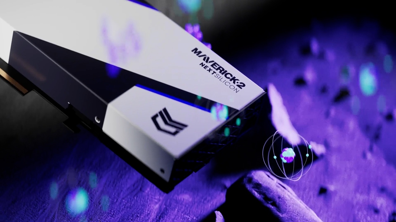
NextSilicon’s Maverick-2 locks onto bottleneck code
- NextSilicon has developed a novel chip that adapts its hardware to accelerate high-performance computing applications.
- The Maverick-2 is claimed to have up to 4x the processing performance per watt of graphics processing units (GPUs) and 20x that of high-performance general processors (CPUs).
After years of work, the start-up NextSilicon has detailed its Maverick-2, what it claims is a new class of accelerator chip.
A key complement to the chip is NextSilicon’s software, which parses the high-performance computing application before mapping it onto the Maverick-2.
“CPUs and GPUs treat all the code equally,” says Brandon Draeger, vice president of marketing at NextSilicon. “Our approach looks at the most important, critical part of the high-performance computing application and we focus on accelerating that.”
With the unveiling of the Maverick-2 NextSilicon has exited its secrecy period.
Founded in 2017, the start-up has raised $303 million in funding and has 300 staff. The company is opening two design centres—in Serbia and Switzerland—with a third planned for India. The bulk of the company’s staff is located in Israel.
High-performance computing and AI
High-performance computing simulates complex physical processes such as drug design and weather forecasting. Such computations require high-precision calculations and use 32-bit or 64-bit floating-point arithmetic. In contrast, artificial intelligence (AI) workloads have more defined computational needs, and can use 16-bit and fewer floating-point formats. Using these shorter data formats results in greater parallelism per clock cycle.
Using NextSilicon’s software, a high-performance computing workload written in such programming languages as C/C++, Fortran, OpenMP, or Kokkos, is profiled to identify critical flows. These are code sections that run most frequently and benefit from acceleration.
“We look at the most critical part of the high-performance computing application and focus on accelerating that,” says Draeger.
This is an example of the Pareto principle: a subset of critical code (the principle’s 20 per cent) that runs most (80 per cent) of the time. The goal is to accelerate these most essential code segments.
The Maverick-2
These code flows are mapped onto the Maverick-2 processor and replicated hundreds or thousands of times, depending on their complexity and the on-chip resources available.
However, this is just the first step. “We run telemetry with the application,” says Draeger. “So, when the chip first runs, the telemetry helps us to size and identify the most likely codes.” The application’s mapping onto the hardware is then refined as more telemetry data is collected, further improving performance.
“In the blink of an eye, it can reconfigure what is being replicated and how many times,” says Draeger. “The more it runs, the better it gets.”
 Source: NextSilicon
The time taken is a small fraction of the overall run time (see diagram). “A single high-performance computing simulation can run for weeks,” says Draeger. “And if something significant changes within the application, the software can help improve performance or power efficiency.”
NextSilicon’s software saves developers months of effort when porting applications ported onto a high-performance computing accelerator, it says.
NextSilicon describes the Maverick-2 as a new processor class, which it calls an Intelligent Compute Accelerator (ICA). Unlike a CPU or GPU, it differentiates the code and decides what is best to speed up. The configurable hardware of the Maverick-2 is thus more akin to a field-programmable gate array (FPGA). But unlike an FPGA, the Maverick-2’s hardware adapts on the fly.
Functional blocks and specifications
The Maverick-2 is implemented using a 5nm CMOS process and is based on a dataflow architecture. Its input-output (I/O) includes 16 lanes of PCI Express (PCIe 5.0) and a 100 Gigabit Ethernet interface. The device features 32 embedded cores in addition to the main silicon logic onto which the flows are mapped. The chip’s die is surrounded by four stacks of high-bandwidth memory (HBM3E), providing 96 gigabytes (GB) of high-speed storage.
NextSilicon is also developing a dual-die design – two Maverick-2s combined – designed with the OCP Acceleration Module (OAM) packaged form factor in mind. The OAM variant, arriving in 2025, will use HBM3E memory for an overall store capacity of 192 gigabytes (GB) (see diagram).
 Source: NextSilicon
The OCP, the open-source industry organisation, has developed an open-source Universal Base Board (OBB) specification that hosts up to eight such OAMs or, in this case, Maverick-2s. NextSilicon is aiming to use the OAM dual-die design for larger multi-rack platforms.
The start-up says it will reveal the devices’ floating-point operations per second (FLOPS) processing performance and more details about the chip’s architecture in 2025.
 Source: NextSilicon

Partners
NextSilicon has been working with vendor Penguin Solutions to deliver systems that integrated their PCI Express modules based on its first silicon, the Maverick-1, a proof-of-concept design. Sandia National Laboratories led a consortium of US labs, including Lawrence Livermore National Laboratory and Los Alamos National Laboratory, in trialling the first design.
“We’re currently sampling dozens of customers across national labs and commercial environments. That’s been our focus,” says Draeger. “We have early-adopter programs that will be available at the start of 2025 with Dell Technologies and Penguin Solutions, where customers can get engaged with an evaluation system.”
Volume production is expected by mid-2025.
Next steps
AI and high-performance computing are seen as two disparate disciplines, but Draeger says AI is starting to interact with the latter in exciting ways.
Customers may pre-process data sets using machine-learning techniques before running a high-performance computing simulation. This is referred to as data cleansing.
A second approach is the application of machine-learning to the simulation’s results for post-processing analysis. Here, the simulation results are used to improve AI models that aim to approximate what a simulation is doing, to deliver results deemed ‘good enough’. Weather forecasting is one application example.
An emerging approach is to run small AI models in parallel with the high-performance simulation. “It offers a lot of promise for longer-running simulations that can take weeks, to ensure that the simulation is on track,” says Draeger.
Customers welcome anything that speeds up the results or provides guidance while the calculations are taking place.
NextSilicon is focussing on HPC but is eyeing data centre computing.
“We’re starting with HPC because that market has many unique requirements, says Draeger. “If we can deliver performance benefits to high-performance computing customers then AI is quite a bit simpler.”
There is a need for alternative accelerator chips that are flexible, power efficient, and can adapt in whatever direction a customer’s applications or workloads take them, says Draeger.
NextSilicon is betting that its mix of software and self-optimising hardware will become increasingly important as computational needs evolve.

Intel sets a course for scalable optical input-output

- Intel is working with several universities to create building-block circuits to address its optical input-output (I/O) needs for the next decade-plus.
- By 2024 the company wants to demonstrate the technologies achieving 4 terabits-per-second (Tbps) over a fibre at 0.25 picojoules-per-bit (pJ/b).
Intel has teamed up with seven universities to address the optical I/0 needs for several generations of upcoming products.
The initiative, dubbed the Intel Research Center for Integrated Photonics for Data Centre Interconnects, began six months ago and is a three-year project.
No new location is involved, rather the research centre is virtual with Intel funding the research. By setting up the centre, Intel’s goal is to foster collaboration between the research groups.
Motivation
James Jaussi, senior principal engineer and director of the PHY Research Lab in Intel Labs, (pictured) heads a research team that focuses on chip-to-chip communication involving electrical and optical interfaces.
“My team is primarily focussed on optical communications, taking that technology and bringing it close to high-value silicon,” says Jaussi.
Much of Jaussi’s 20 years at Intel has focussed on electrical I/O. During that time, the end of electrical interfaces has repeatedly been predicted. But copper’s demise has proved overly pessimistic, he says, given the advances made in packaging and printed circuit board (PCB) materials.
But now the limits of copper’s bandwidth and reach are evident and Intel’s research arm wants to ensure that when the transition to optical occurs, the technology has longevity.
“This initiative intends to prolong the [optical I/O] technology so that it has multiple generations of scalability,” says Jaussi. And by a generation, Jaussi means the 3-4 years it takes typically to double the bandwidth of an I/O specification.
Co-packaged optics and optical I/O
Jaussi distinguishes between co-packaged optics and optical I/O.
He describes co-packaged optics as surrounding a switch chip with optics. Given the importance of switch chips in the data centre, it is key to maintain compatibility with specifications, primarily Ethernet.
But that impacts the power consumption of co-packaged optics. “The power envelope you are going to target for co-packaged optics is not necessarily going to meet the needs of what we refer to as optical I/O,” says Jaussi.
Optical I/O involves bringing the optics closer to ICs such as CPUs and graphics processor units (GPUs). Here, the optical I/O need not be aligned with standards.
The aim is to take the core I/O off a CPU or GPU and replace it with optical I/O, says Jaussi.
With optical I/O, non-return-to-zero (NRZ) signalling can be used rather than 4-level pulse amplitude modulation (PAM-4). The data rates are slower using NRZ but multiple optical wavelengths can be used in parallel. “You can power-optimise more efficiently,” says Jaussi.
Ultimately, co-packaged optics and optical I/O will become “stitched together” in some way, he says.
Research directions
One of the research projects involves the work of Professor John Bowers and his team at the University of California, Santa Barbara, on the heterogeneous integration of next-generation lasers based on quantum-dot technology.
Intel’s silicon photonics transceiver products use hybrid silicon quantum well lasers from an earlier collaboration with Professor Bowers.
The research centre work is to enable scalability by using multi-wavelength designs as well as enhancing the laser’s temperature performance to above 100oC. This greater resilience to temperature helps the laser’s integration alongside high-performance silicon.
Another project, that of Professor Arka Majumdar at the University of Washington, is to develop non-volatile reconfigurable optical switching using silicon photonics.
“We view this as a core building block, a capability,” says Jaussi. The switching element will have a low optical loss and will require liitle energy for its control.
The switch being developed is not meant to be a system but an elemental building block, analogous to a transistor, Intel says, with the research exploring the materials needed to make such a device.
The work of Professor S.J. Ben Yoo at University of California, Davis, is another of the projects.
His team is developing a silicon photonics-based modulator and a photodetector technology to enable 40-terabit transceivers at 150fJ/bit and achieving 16Tb/s/mm I/O density.
“The intent is to show over a few fibres a massive amount of bandwidth,” says Jaussi.
Goals
Intel says each research group has its own research targets that will be tracked.
All the device developments will be needed to enable the building of something far more sophisticated in future, says Jaussi.
At Intel Labs’ day last year, the company spoke about achieving 1Tbps of I/O at 1pJ/s. The research centre’s goals are more ambitious: 4Tbps over a fibre at 0.25pJ/b in the coming three years.
There will be prototype demonstrations showing data transmissions over a fibre or even several fibres. “This will allow us to make that scalable not just for one but two, four, 10, 20, 100 fibres,” he says. “That is where that parallel scalability will come from.”
Intel says it will be years before this technology is used for products but the research goals are aggressive and will set the company’s optical I/O goals.