
oDAC: Boosting data centre speeds with less power

Academics have developed an optical digital-to-analogue converter (oDAC) that promises to rethink how high-speed optical transmission is done.
Conceived under the European Commission-funded Flex-Scale project for 6G front-haul, the oDAC also promises terabit links inside the data centre.
The oDAC is expected to deliver a 40 per cent power savings for a 1.6 terabit optical transmitter, the ‘send’ path of an optical module.
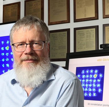
“It might not be not 50 or 60 per cent, but in this field, even a 25 per cent power saving turns heads,” says Ioannis Tomkos, a professor at the Department of Electrical and Computer Engineering at the University of Patras, Greece, one of the researchers leading the work.
The first proof-of-concept oDAC photonic integrated circuit (PIC) has sent 250 gigabits per second (Gbps) over a single wavelength as part of the European Proteus programme.
The goal is to bring the oDAC to market in 2026.
High-speed optical transmission challenges
An optical interface acts as a gateway between the electrical and optical domains.
The main two classes of optical interfaces—pluggable modules for the data centre and coherent designs for longer-distance links—continue to grow in data rate.
The upcoming rate today is 1.6 terabits per second (Tbps), with 3.2Tbps optical links are in development. But going faster adds design complexity and consumes extra power.
Faster electrical signalling must use encoding schemes such as 4-level pulse amplitude modulation (PAM-4). And in the optical domain, PAM-4 is used in the data centre while higher-order modulation schemes such as 16-ary quadrature amplitude modulation (16-QAM) are used for long-haul optical transmissions. Quadrature amplitude modulation uses amplitude and phase modulation thyat doubles transmission capacity.
Such schemes require fast analogue-to-digital converters (ADCs), digital-to-analogue converters (DACs), and digital signal processing (DSPs) to compensate for transmission impairments. But as speeds increase, so does the signalling complexity and sampling rates, driving up the overall cost and power consumption.
The trends are leading researchers to consider alternative approaches, such as signal processing in the optical domain, to lessen the demands placed on the DSP and its DACs and ADCs. Researchers are even wondering if such an approach could remove the DSP altogether.
“Step by step,” cautions Tomkos.
Tomkos is working with Professor Moshe Nazarathy, a founder of the oDAC work, at the Faculty of Electrical Engineering at Technion University, Israel.
And it is developing the oDAC where they have first focussed their efforts.
Electronic DAC versus the oDAC
One way to view the oDAC is as a high-speed optical modulator. Another is as a multiplexer of multiple optical amplitude data streams.
The oDAC is a fundamental building block that trades extra optical components to simplify the electrical drivers for the high-speed transmitter. This is how the 40 per cent power saving is achieved.
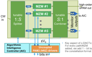
The oDAC’s architecture is similar to that of a coherent optical transmitter but with notable differences.

In a coherent optical transmitter setup, the laser source is split evenly to feed the in-phase and quadrature Mach-Zehnder modulators (MZMs), with a 90-degree phase shifter in one of the modulator’s arms (see diagram above, left).
In contrast, the oDAC employs a variable splitter and a combiner at the input and output stages, paired with identical Mach-Zehnder modulators (no phase shifter is used in one of the modulator’s arms, see diagram, right). The ODACs can be used in a nested arrangement, as part of in-phase and quadrature arms, for coherent optical transmission.
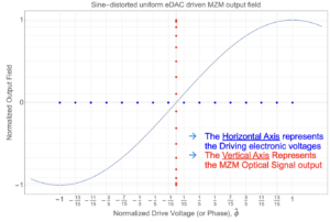
Conventional electronic DACs (eDACs in the diagram) sample the data at least as high as the symbol rate and have a finite bit resolution, which limits the higher-order modulation schemes that can be used.
They are used to drive the optical Mach-Zehnder modulator, which has a non-linear sine-shaped response. The non-linearity forces the modulator to work only in the linear region of its transfer function. (See graph below.)

This curtailing of the driver saves power but results in ‘modulator loss’ – the full potential of the modulator is not being used, impacting signal recovery at the optical receiver.
In contrast, the oDAC can drive fully the modulator, thereby avoiding the modulator backoff loss.
Another key oDAC benefit is that each of its Mach-Zehnder modulators is driven using simpler PAM driver chips to produce higher-order PAM signals: two standard PAM-4 drivers can produce PAM-16 and using two oDAC PAM-16s can be used to generate PAM-256 (each symbol carrying 4- or 8-bits, respectively).
No commercial electronic PAM-16 drivers exist, says Tomkos.
Scaling data rates using PAM-4 drivers
A PAM-4 driver for the oDAC’s Mach-Zehnder modulator arm produces a four-level “staircase” waveform. Adjusting the oDAC’s splitter ratio to 4:1 and summing the outputs yields 16 distinct levels (diagram, below)

n effect, two simple signals can be stacked in multiple combinations to mimic a complex one. For PAM-16, one Mach-Zehnder modulator handles levels 0, 1, 2, and 3, while the other one, scaled differently (e.g., 0, 4, 8, 12), ensures a sum from 0 to 15.
The catch? Achieving a smooth staircase signal requires precise in-phase combining and level controls so there are no differences between the two Mach-Zehnder arms, which requires careful circuit control.
“Every programmable photonic circuit in general, for whatever application, needs some parametric control of the actual circuit,” says Tomkos. “For our case, it is so that it will not deviate if you change the temperature if you have vibrations or any other environmental changes.”

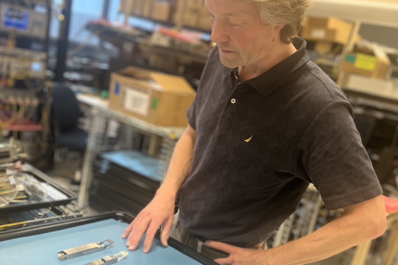
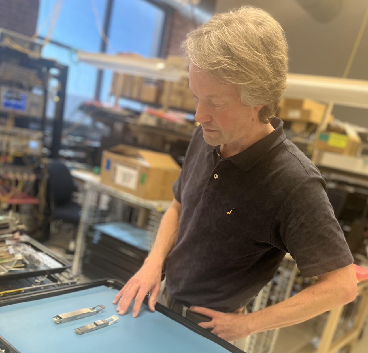
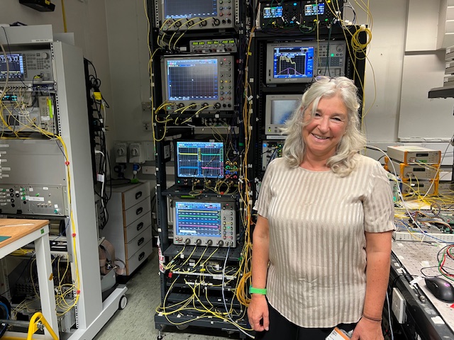
David Moor, a post-doctorate researcher at ETH-Zürich, part of the Flex-Scale project, and the director of photonic IC design at Emitera, the start-up tasked with bringing the oDAC to market, has been putting the prototype oDAC photonic integrated circuit through lab tests.
To send 500 Gbps over a single wavelength, a two-arm oDAC is used, with each PAM4-driven arm operating at 120 gigabaud symbol rate, or 250Gbps. While using two oDACs feeding an in-phase and quadrature coherent structure, doubles the data rate to 1Tbps.
Then, using a pair of PAM-16 oDACs (each driven by a pair of PAM-4 signals, in-phase and quadrature-combined in a coherent transmitter structure, further doubles the data rate to 1.6Tbps.

Transmissions at 3.2 terabits would need the symbol rate at 240 GBd.
What next?
Professor Nazarathy, working with Professor Birbas and his team at the University of Patras, are developing an FPGA-based control system to ensure the device operates optimally in real-world conditions.
“In the lab, the device has been quite stable,” says Moor. But any environmental changes throw it off track. oDAC device needs robust control to be a commercial product.
A second-generation oDAC photonic integrated circuit design and an FPGA-based control system are in the works and are expected to be up and running in six months.
Applications: Data centres and front-haul
“The higher-order the modulation format used, from 16-QAM to 256-QAM, the less the distance,” says Tomkos. “This is a law of information theory. You cannot do otherwise; nobody can.”
But the benefit of the design grows the higher the modulation order and the higher bit rate. Thus, the oDAC comes into its own when using 16-QAM and higher-order signalling schemes.
Accordingly, the ODAC’s sweet spot is for links up to 20 or even 40km, where terabits of data can be pushed over an optical wavelength. This makes the oDAC concept ideal for “coherent-lite” spans between campuses and when used inside the data centre.
The long game: Acacia's coherent vision
In 2007, Christian Rasmussen made a career-defining gamble. After attending a conference featuring presentations on coherent optical transmission, he returned home, consulted his family, and quit his job at Mintera, then an optical networking equipment maker.
The technology he’d seen discussed promised to solve the transmission impairments associated with direct-detection-based optical transmission – chromatic dispersion and polarisation mode dispersion – that had stymied optical transport to go beyond 40 gigabits-per-second (Gbps).
“We came back and were completely excited that there was a technology that addressed all the problems that we had experienced firsthand,” says Rasmussen, now Chief Technology Officer at Acacia.
His bet paid off. Acacia which he helped co-found in 2009, had a successful IPO in 2016 and would later be acquired by Cisco Systems for $4.5 billion in 2021.
Unfolding coherent optics
Increasing the baud rate has proved spectacularly successful in accommodating traffic growth in the network and reducing transport costs measured in dollar-per-bit.
In 2009, coherent modems operated around 32 gigabaud (GBd) for 100 gigabit-per-second (Gbps) wavelength transmissions. By 2024, the symbol rate has reached 200GBd, enabling 1.6 terabit-per-second (Tbps) wavelengths.
Is the priority still to keep upping the symbol rate of a single carrier when designing next-generation coherent modems?
“We are not just saying that increasing baud rate is right,” says Rasmussen. The fundamental goal is reducing optical transport’s cost and power consumption. “Increasing the baud rate is generally the right approach to achieve that goal but it’s always to a certain degree.”
Acacia’s focus from the beginning has been on integrating the components that make up the coherent modem. The resulting modem need not be expensive and can deliver higher speed and extra bandwidth economically while meeting the power consumption target, he says.
“Until now, we feel that increasing the baud rate has been the right approach,” says Rasmussen. “The question will be how frequently you can go up in baud rate, now that developments are expensive.”
Given the rising cost of developing coherent modems, upping the baud rate only makes sense if designers can double it with each new design, he says. Increasing the baud rate by 30 or 40 percent is too small a return, given the development effort and the costs involved.
That implies Acacia’s follow-on high-end coherent modem will have a symbol rate of around 280GBd.
Acacia’s coherent modules
Acacia’s Coherent Interconnect Module 8 (CIM 8), launched in 2021, was the industry’s first single-carrier 1.2Tbps pluggable module. The module operates at a 140GBd symbol rate.
At ECOC 2024, the company showcased its 800 gigabit ZR+ OSFP pluggable modules, featuring the Delphi coherent DSP implemented in 4nm CMOS process.
The module supports up to 131GBd and implements interoperable probabilistic constellation shaping. The Acacia module has C-band and L-band variants and supports ultra-long-haul distances when sending 400Gbps over a single carrier (see Table).

Challenges and opportunities
The path forward presents challenges and opportunities. There are several design considerations when developing a coherent DSP ASIC.
One is choosing what CMOS process to use. Considerations include cost – the smaller the geometry the more expensive the design, the transistors’ switching speed, whether the chip’s resulting power consumption is acceptable, and the CMOS process’s maturity. If the process is under development, what confidence is there that it will deliver the promised performance once the ASIC design is completed and ready for manufacturing?
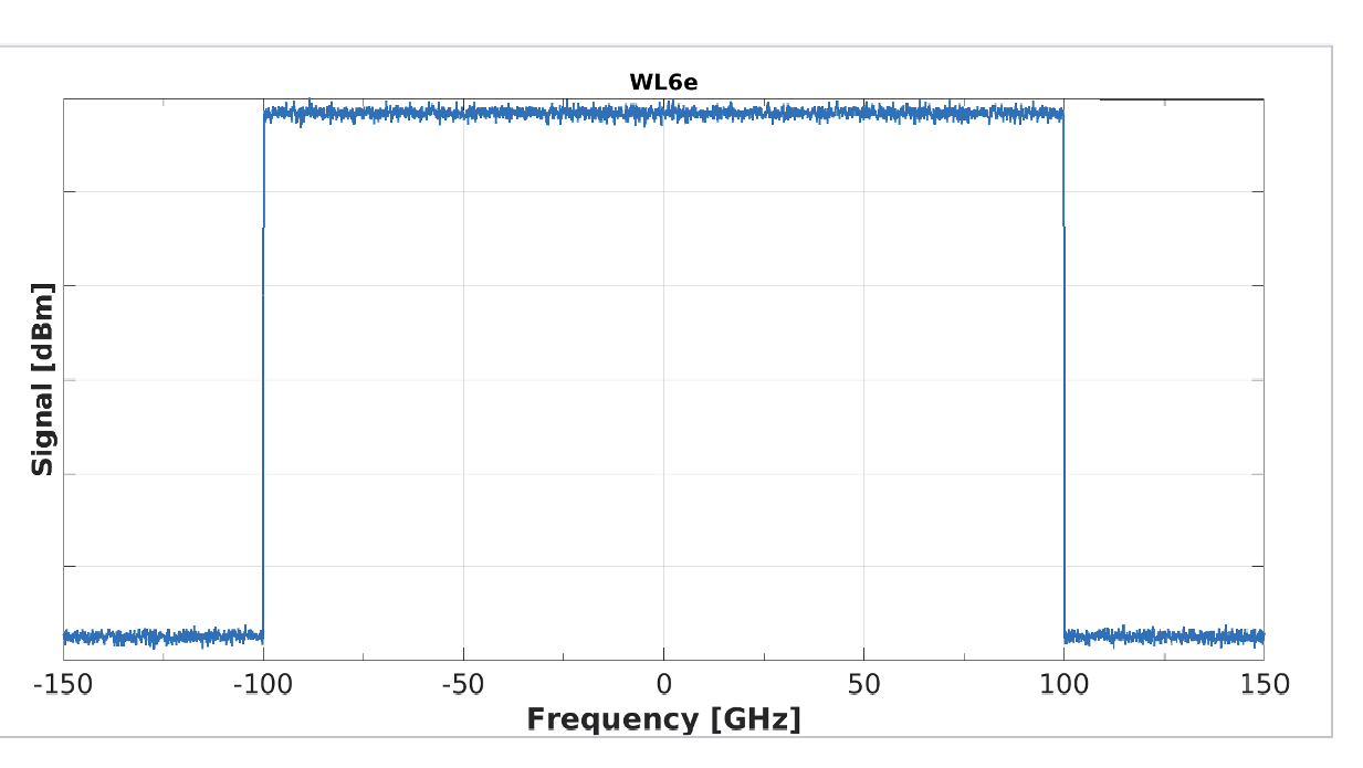
The state-of-the-art CMOS process used for coherent DSPs is 3nm. Ciena’s 200GBd WaveLogic 6e is the first coherent DSP to ship using a 3nm CMOS process. Rasmussen is confident that a 3nm CMOS process can achieve at least a 250GBd symbol rate.
Another consideration is to ensure that the DSP’s analogue-to-digital converters (ADCs) and digital-to-analogue converters (DACs) can achieve the required sampling speed and quality. Typically, the ADC sample at 1.1x-1.2x the baud rate, which, for a 250GBd symbol rate, equates to the order of 300 giga-samples a second (GS/s). Achieving such speeds is exceptionally challenging.
Some research is exploring other ways to keep boosting converter sampling speed. One idea is to split the converter’s design between the DSP and a higher-bandwidth III-V material used for the driver or receiver circuitry.
Rasmussen stresses that the key is to keep the ADCs and DACs in CMOS as a part of the DSP. “Once you start going there [splitting the DAC and ADC designs], you start risking your cost and power advantage of the single-carrier approach,” he says.
Acacia timeline
- 2007: Rasmussen attends pivotal conference on coherent transmission
- 2009: Acacia founded; 32GBd coherent modems achieve 100Gbps
- 2014: Acacia is first to ship samples of a coherent pluggable 100G CFP module and announced the industry’s first 100G coherent transceiver in a single silicon photonics integrated circuit package
- 2021: Cisco acquires Acacia for $4.5 billion
- 2021: Launch of CIM 8 (140GBd, 1.2Tbps)
- 2024: Acacia showcases its 800ZR+ OSFP module
Team-oriented approach
As CTO, Rasmussen emphasises the importance of working with colleagues to make decisions. “I’m very passionate about this: team-oriented decision-making,” he says. His role involves extensive conversations with product managers and colleagues that interact with customers to understand market needs, alongside technical discussions and conference attendance to guide technology development.
This collaborative approach has shaped Acacia’s integration strategy as well as the company becoming more vertically integrated. “Owning the whole stack so you always have everything in control,” as Rasmussen puts it, has proven crucial to their success.

From Denmark to Cisco
Rasmussen’s journey began in Denmark, where he completed his electrical engineering degree and doctorate in optical communications before moving to Boston. There, he joined Benny Mikkelsen, now Acacia’s senior vice president and general manager, at Mintera, where they grappled with the limitations of pre-coherent optical systems.
The struggle with 40Gbps direct-detect optical transport systems ultimately led to that pivotal moment in 2007. “It did not make much commercial sense to struggle so much to get to 40 gigabits,” Rasmussen recalls. When coherent transmission emerged as a solution, he and his colleagues seized the opportunity, despite the industry’s post-dot-com bubble and the 2008 financial crisis.
He began working with Mikkelsen and Mehrdad Givehchi on business plans and developing the technology. “Digital signal processing was new to us, so there was a lot of stuff to learn,” he says.
After being turned down by numerous venture capital firms, one – Matrix Parners- backed the Acacia team, which also received corporate funding from OFS, part of Furukawa Electric.
Beyond Technology
Outside the lab, Rasmussen finds balance in gardening, appreciating its immediate rewards compared to the years-long cycle of DSP design. “It’s nice to do something where you can see the immediate result of your work,” he says.
His interests also extend to reading. He recommends “Right Hand, Left Hand” by Chris McManus, praising its exploration of symmetry in nature, and “The Magic of Silence” by Florian Illies, which examines the enduring relevance of painter Caspar David Friedrich.
Looking ahead, Rasmussen remains optimistic about the industry’s innovative capacity.
He says that semiconductor foundries do not tend to publicise their CMOS transistors’ switching frequency, but it is already above 500GHz and approaching 1,000GHz. This suggests that a DSP supporting a baud rate of 400GBd will be possible. And four to five years hence, two more generations of CMOS after 3nm are likely. This all suggests that a further doubling of baud rate to 500GBd is feasible.
“Just look at the record of innovation at Acacia and other companies in the industry; people keep coming up with solutions,” says Rasmussen.

The OIF's coherent optics work gets a ZR+ rating
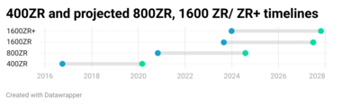
The OIF has started work on a 1600ZR+ standard to enable the sending of 1.6 terabits of data across hundreds of kilometres of optical fibre.The initiative follows the OIF's announcement last September that it had kicked off 1600ZR. ZR refers to an extended reach standard, sending 1.6 terabits over an 80-120km point-to-point link.
600ZR follows the OIF’s previous work standardising the 400-gigabit 400ZR and the 800-gigabit 800ZR coherent pluggable optics.
The decision to address a ‘ZR+’ standard is a first for the OIF. Until now, only the OpenZR+ Multi-Source Agreement (MSA) and the OpenROADM MSA developed interoperable ZR+ optics.
The OIF’s members’ decision to back the 1600ZR+ coherent modem work was straightforward, says Karl Gass, optical vice chair of the OIF’s physical link layer (PLL) working group. Several companies wanted it, and there was sufficient backing. “One hyperscaler in particular said: ‘We really need that solution’,” says Gass.
OIF, OpenZR+, and OpenROADM
Developing a 1600ZR+ standard will interest telecom operators who, like with 400ZR and the advent of 800ZR, can take advantage of large volumes of coherent pluggables driven by hyperscaler demand. However, Gass says no telecom operator is participating in the OIF 1600ZR+ work.
“It appears that they are happy with whatever the result [of the ZR+ work] will be,” says Gass. Telecom operators are active in the OpenROADM MSA.
Now that the OIF has joined OpenZR+ and the OpenROADM MSA in developing ZR+ designs, opinions differ on whether the industry needs all three.
“There is significant overlap between the membership of the OpenZR+ MSA and the OIF, and the two groups have always maintained positive collaboration,” says Tom Williams, director of technical marketing at Acacia, a leading member of the OpenZR+. “We view the adoption of 1600ZR+ in the OIF as a reinforcement of the value that the OpenZR+ has brought to the market.”
Robert Maher, Infinera’s CTO, believes the industry does not need three standards. However, having three organisations does provide different perspectives and considerations.
Meanwhile, Maxim Kuschnerov, director R&D at Huawei, says the OIF’s decision to tackle ZR+ changes things.”OpenZR+ kickstarted the additional use cases in the industry, and OpenROADM took it away but going forward, it doesn’t seem that we need additional MSAs if the OIF is covering ZR+ for Ethernet clients in ROADM networks,” says Kuschnerov. “Only the OTN [framing] modes need to be covered, and the ITU-T can do that.”
Kuschnerov also would like more end-user involvement in the OIF group. “It would help shape the evolving use cases and not be guided by a single cloud operator,” he says.
ZR history
The OIF is a 25-year-old industry organisation with over 150 members, including hyperscalers, telecom operators, systems and test equipment vendors, and component companies.
In October 2016, the OIF started the 400ZR project, the first pluggable 400-gigabit Ethernet coherent optics specification. The principal backers of the 400ZR work were Google and Microsoft. The standard was designed to link equipment in data centres up to 120km apart.
The OIF 400ZR specification also included an un-amplified version with a reach of several tens of kilometres. The first 400ZR specification document, which the OIF calls an Implementation Agreement, was completed in March 2020 (see chart above).
The OIF started the follow-up on the 800ZR specification in November 2020, a development promoted by Google. Gass says the OIF is nearing completion of the 800ZR Implementation Agreement document, expected in the second half of 2024.
If the 1600ZR and ZR+ coherent work projects take a similar duration, the first 1600ZR and 1600ZR+ products will appear in 2027.
Symbol rate and other challenges
Moving to a 1.6-terabit coherent pluggable module using the same modulation scheme – 16-ary quadrature amplitude modulation or 16-QAM – used for 400ZR and 800ZR suggests a symbol rate of 240 gigabaud (GBd).
“That is the maths, but there might be concerns with technical feasibility,” says Gass. “That’s not to say it won’t come together.”
The highest symbol rate coherent modem to date is Ciena’s WaveLogic 6e, which was announced a year ago. The design uses a 3nm CMOS coherent digital signal processor (DSP) and a 200GBd symbol rate. It is also an embedded coherent design, not one required to fit inside a pluggable optical module with a constrained power consumption.
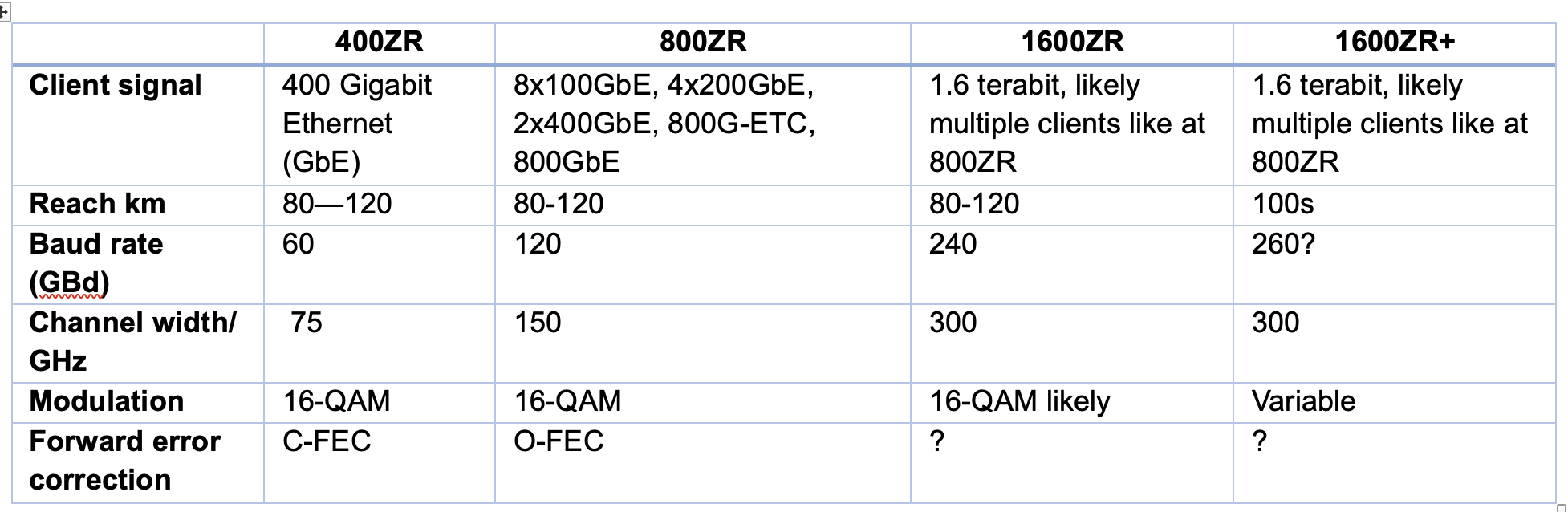
Kuschnerov points out that the baud rates of ZR and ZR+ have differed. And this will likely continue. 800ZR, using Ethernet with no probabilistic constellation shaping, has a baud rate of 118.2GBd, while 800ZR+, which uses OTN and probabilistic constellation shaping, has a baud rate of up to 131.35GBd. Every symbol has a varying probability when probabilistic constellation shaping is used. “This decreases the information per symbol, and thus, the baud rate must be increased,“ says Kuschnerov.
Doubling up for 1600ZR/ ZR+, those numbers become around 236GBd and 262GBd, subject to future standardisation. “So, saying that 1600ZR is likely to be at 240GBd is correct, but one cannot state the same for a potential 1600ZR+,” says Kuschnerov.
Nokia’s view is that for 1600ZR, the industry will look at operating modes that include 16QAM at 240 GBd. Other explored options include 64-QAM with probabilistic constellation shaping at 200GBd and even dual optical carrier solutions with each carrier operating at approximately 130GBd. “However, this last option may be challenging from a power envelope perspective,” says Szilárd Zsigmond, head of Nokia’s optical subsystems group.
In turn, if 1600ZR+ reaches 1,000km distances, the emphasis will be on higher baud rate options than those used for 1600ZR. “This will be needed to enable longer reaches, which will also put pressure on managing power dissipation,” says Zsigmond.
The coherent DSP must also have digital-to-analogue (DACs) and analogue-to-digital converters (ADCs) to sample at least at 240 giga-samples per second. Indeed, the consensus among the players is that achieving the required electronics and optics will be challenging.
“All component bandwidths have to double and that is a significant challenge,” says Josef Berger, associate vice president, cloud optics marketing at Marvell.
The coherent optics – the modulators and receivers – must extend their analogue bandwidth of 120GHz. Infinera is one company that is confident this will be achieved. “Infinera, with our highly integrated Indium Phosphide-based photonic integrated circuits, will be producing a TROSA [transmitter-receiver optical sub-assembly] capable of supporting 1.6-terabit transmission that will fit in a pluggable form factor,” says Maher.
The coherent DSP and optics operating must also meet the pluggable modules’ power and heat limits. “That is an extra challenge here: the development needs to maintain focus on cost and power simultaneously to bring the value network operators need,” says Williams. “Scaling baud rate by itself doesn’t solve the challenge. We need to do this in a cost and power-efficient way.”
Current 800ZR modules consume 30W or more, and since the aim of ZR modules is to be used within Ethernet switches and routers, this is challenging. In comparison, 400ZR modules now consume 20W or less.
“For 800ZR and 800ZR+, the target is to be within the 28W range, and this target is not changing for 1600ZR and 1600ZR+,” says Zsigmond. Coherent design engineers are being asked to double the bit rate yet keep the power envelope constant.
Certain OIF members are also interested in backward compatibility with 800ZR or 400ZR. “That also might affect the design,” says Gass.
Given the rising cost to tape out a coherent DSP using 3nm and even 2nm CMOS process nodes required to reduce power per bit, most companies designing ASICs will look to develop one design for the 1600ZR and ZR+ applications to maximise their return on investment, says Zsigmond, who notes that the risk was lower for the first generations of ZR and ZR+ applications. Most companies had already developed components for long-haul applications that could be optimised for ZR and ZR+ applications.
For 400ZR, which used a symbol rate of 60 GBd, 60-70 GBd optics already existed. For 800 gigabit transmissions, high-performance embedded coherent optics and pluggable, low-power ZR/ZR+ modules have been developed in parallel. “For 1600ZR/ZR+, it appears that the pluggable modules will be developed first,” says Zsigmond. “There will be more technology challenges to address than previous ZR/ZR+ projects.”
The pace of innovation is faster than traditional coherent transmission systems and will continue to reduce cost and power per bit, notes Marvell’s Berger: “This innovation creates technologies that will migrate into traditional coherent applications as well.”
Gass is optimistic despite the challenges ahead: “You’ve got smart people in the room, and they want this to happen.”
OIF's OFC 2024 demo
The OIF has yet to finalise what it will show for the upcoming coherent pluggable module interoperable event at OFC to be held in San Diego in March. But there will likely be 400ZR and 800ZR demonstrations operating over 75km-plus spans and 400-gigabit OpenZR+ optics operating over greater distance spans.
Optical networking's future
Should the industry do more to support universities undertaking optical networking research? Professor Polina Bayvel thinks so and addressed the issue in her plenary talk at the ECOC conference and exhibition held in Glasgow, Scotland, earlier this month.
In 1994, Bayvel set up the Optical Networks Group at University College London (UCL). Telecom operators and vendors like STC, GPT, and Marconi led optical networking research. However, setting up the UCL’s group proved far-sighted as industry players cut their research budgets or closed.
Universities continue to train researchers, yet firms do not feel a responsibility to contribute to the costs of their training to ensure the flow of talent. One optical systems vendor has hired eight of her team.
In her address, Bayvel outlined how her lab should be compensated. For example, when a club sells a soccer player, the team that developed him should also get part of the fee.
Such income would be welcome, says Bayvel, citing how she has a talented student from Brazil who needs help to fund his university grant. Her lab would also benefit. During a visit, a pile of boxes – state-of-the-art test equipment – had just arrived.
Plenary talk
Bayvel mentioned how the cloud didn’t exist 18 years ago and that what has enabled it is optical networking and Moore’s law. She also tackled how technology will likely evolve in the next 18 years.
Digital data is being created at a remarkable rate, she said. Three exabytes (a billion billion bytes) are being added to the cloud, which holds several zettabytes (1,000 exabytes or ZB) of data. By 2025, data in the cloud will be 275ZB.
The cited stats continued: 6.2 billion kilometres of fibre have been deployed between 2005 and 2023, having 60Zbits of capacity. In comparison, all data satellite systems now deployed offer 100Tb, less than the capacity of one fibre.
Moore’s law has enabled complex coherent digital signal processors (DSPs) that clean up the distortions of an optical signal sent over a fibre. The first coherent DSPs consumed 1W for each gigabit of data sent. Over a decade later, DSPs use 0.1W to send a gigabit.
Data growth will keep driving capacity, says Bayvel. Engineers have had to fight hard to squeeze more capacity using coherent optical technology. Further improvement will come from techniques such as non-linear compensation. One benefit of Moore’s law is that coherent DSPs will be more capable of tasks such as non-linear compensation. For example, Ciena’s latest 3nm CMOS process, the WaveLogic 6e DSP, uses one billion digital logic gates.
Extra wide optical comms
But only so much can be done by the DSP and increasing the symbol rate. The next step will be to ramp the bandwidth by combining a fibre’s O, S, C, L, E and U spectrum bands. New optical devices, such as hybrid amplifiers, will be needed, and pushing transmission distance over these bands will be hard.
“We fought for fractions of a decibel [of signal-to-noise ratio]; surely we’re not going to give up the wavelengths available through this [source of] bandwidth?” said Bayvel.
In his Market Focus talk at ECOC, BT’s Professor Andrew Lord argued the opposite. There will be places where combining the C- and L-bands will make sense, but why bother when spatial division multiplexing fibre deployments in the network are inevitable, he said.
“It is not spatial division multiplexing versus extra wide optical comms; they can co-exist,” said Bayvel.
Bayvel describes work to model the performance of such a large amount of spectrum that has been done in her lab using data collected from the MAREA sub-sea cable. Combining the fibre’s spectral bands – a total of 60 terahertz of spectrum – promises to quadruple the bandwidth currently available. However, this will require more powerful DSPs than are available today.
Another area ripe for development is intelligent optical networking using machine learning.
An ideas lag
Bayvel used her talk to pay tribute to her mentor, Professor John Midwinter.
Midwinter was an optical communications pioneer at BT and then UCL. He headed the team that developed the first trial systems that led to BT becoming the first company in the world to introduce optical fibre communications systems in the network.
In 1983, his last year at BT, Midwinter wrote in the British Telecom Technology Journal that this was the year coherent optical systems would be taken seriously. It took another 20-plus years.
Bayvel noted how many ideas developed in optical research take considerable time before the industry adopts them. “Changes in the network are much slower,” she said. “Operators are conservative and focus on solving today’s problems.”
Another example she cited is Google’s Apollo optical switch being used in its data centres. Bayvel noted that the switch is relatively straightforward, using MEMS technology that has been around for 25 years.
Bayvel used her keynote to attack the telecom regulators.
“It is simply unfair that the infrastructure providers get such a small part of the profits compared to the content providers,” she said. “The regulators have done a terrible job.”
How DSP smarts continue to improve optical transport
- Kim Roberts explains the signal processing techniques Ciena is using for its WaveLogic 6 coherent DSP.
- Roberts explains how the techniques squeeze, on average, a 15 per cent improvement in spectral efficiency.
- The WaveLogic 6 Extreme chip can execute 1,600 trillion (1.6 x 10¹⁵) operations per second and uses the equivalent of 4km of on-chip copper interconnect.
Part 2: WaveLogic 6’s digital signal processing toolkit
Bumping into Kim Roberts on the way to the conference centre at OFC, held in San Diego in March, I told him how, on the Ciena briefing about its latest WaveLogic 6 coherent digital signal processor (DSP), there had been insufficient time to dive deeply into the signal processing techniques used.
“What are you doing now?” said Roberts.
“I’m off to the plenary session to catch the keynotes.”
Chatting some more, I realised I was turning down a golden opportunity to sit down with a leading DSP and coherent modem architect.
“Is that offer still open?” I asked.
He nodded.
We grabbed a table at a nearby cafe and started what would prove to be an hour-long conversation.
High-end coherent DSPs
Many leading coherent modem vendors unveiled their latest designs in the run-up to the OFC show. It is rare for so many announcements to be aligned, providing a valuable glimpse of the state of high-performance optical transport.
Nokia announced its PSE-6s, which has a symbol rate of up to 130 gigabaud (GBd) and supports 1.2 terabit wavelengths. Infinera announced its 1.2-terabit ICE-7, which has a baud rate of up to 148GBd, while Fujitsu detailed it is using its 135GBd 1.2-terabit wavelength coherent DSP for its 1FINITY Ultra optical platform.
Meanwhile, Acacia, a Cisco company, revealed its 140GBd Jannu 1.2-terabit DSP has been shipping since late 2022. Acacia announced the Jannu DSP in March 2022.
All these coherent DSPs are implemented using 5nm CMOS and are shipping or about to.
And Ciena became the first company to detail a coherent DSP fabricated using a 3nm CMOS process. The WaveLogic 6 Extreme supports 1.6-terabit wavelengths and has a symbol rate of up to 200GBd.
Ciena’s WaveLogic 6 Extreme improves spectral efficiency by, on average, 15 per cent. WaveLogic 6 Extreme-based coherent modems will be available from the first half of 2024.
Customer considerations
Kim Roberts begins by discussing what customers want.
“With terrestrial systems, it is cost-per-bit [that matters], and if you’re not going very far, it is cost-per-modem,” says Roberts.
For the shortest reaches (tens of km), 100 gigabit may be enough while 200 gigabit or more is overkill. Here, a coherent pluggable module does the job.
“What matters is the cost per modem to get the flexibility of coherent connectivity so that you can plug it in and it works,” says Roberts.
With medium and long-haul terrestrial routes, cost-per-bit and heat-per-bit are the vital issues. With heat, area and volume of the coherent design are important. “I need volume to get the heat out of the chip on the card and into the air,” says Roberts.
Another use case is where spectral efficiency is key, for networks where fibre is scarce. An operator could be leasing dark fibre, or it could be a submarine network.
Ciena’s WaveLogic 6 Extreme’s 15 per cent improvement in spectral efficiency improves capacity over the same link. “Equivalently, you can go a dB (decibel) further or have a dB more signal margin,” says Roberts.
A common refrain heard is that spectral efficiency is no longer improving due to the Shannon limit being approached. Shannon’s limit is being approached because of the considerable progress already made by the industry in coherent optics.
“There is no 6dB to be had like in the old days,” says Roberts. “WaveLogic 3 was 2.5dB better than WaveLogic 2, but those multiple dBs are no longer there.”
The returns are diminishing, but striving for improvements remains worthwhile. “If you’re an operator that cares about spectral efficiency, that’s important,” he says.
Nonlinearity mitigation
Roberts returns to the issue of Shannon’s limit, based on the work of famed mathematician and information theorist, Claude Shannon.
“Shannon defines a theoretical limit for the capacity of a channel having linear propagation with additive Gaussian noise,” says Roberts.
This defines a strict mathematical limit, and it is pointless to go beyond that; he says: “In terms of linear performance, modems are getting close to the limit, within a couple of dB.”
Shannon’s limit doesn’t wholly define fibre since the channel is nonlinear.
Roberts says there is a whole research area addressing the bounds given such nonlinearities.
“We’re a long way from those theoretical nonlinear limits, but what matters is what’s the practical limit, and it’s getting hard,” he says
Increasing transmit power improves the optical signal-to-noise ratio (OSNR) and strengthens nonlinearities. Indeed, the nonlinearities grow faster with increased transmit power until, eventually, they dominate.
Because tackling nonlinearities is so complicated, Ciena’s approach is to approximate the problem as a linear Gaussian noise channel and do everything possible to mitigate the effects of nonlinearity rather than embrace it.
This is done by compensating at the transmitter the nonlinearities expected to happen along the fibre. The receiver performs measurements on a second-by-second basis and sends the results back. These are used as estimates of the anticipated nonlinearity about to be encountered and subtracted from the symbols to be sent.
Even though the exact nonlinearity is unknown, this is still a valid approximation. “It gives a quarter to one dB of performance improvement,” says Roberts
Edgeless clock recovery
Robert explains other clever signal processing techniques that buy a 6 per cent spectral efficiency improvement.
With wavelength division multiplexing (WDM), the laser-generated signals are placed next to each other across the fibre’s spectrum.
For WaveLogic 6, when running at its maximum symbol rate of 200 gigabaud, the spectrum occupies a 200GHz-wide channel.
Usually, the signal in the frequency domain is not perfectly square-shaped; the signal rolls off in the frequency domain so that in the time domain there is no inter-symbol interference. “But [as a result] you’re wasting spectrum; you are not fully using that spectrum,” says Roberts.
With WaveLogic 6, Ciena has created an idealised flat-topped, vertically edged signal spectra allowing the signals to be crammed side by side thereby making best use of the fibre’s spectrum (see diagram).
The challenge is that the clocking information used for data recovery at the receiver resided in this roll-off region. Now, that is no longer there so Cienahas developed another method to recover clock information.
A second challenge with signal recovery is that the transmit laser and the receive laser are not rigidly fixed in frequency. Being so close together, care is needed to recover only the wavelength – signal – of interest.
Yet another complication is how a rectangle in the frequency domain causes the signal in the time domain to ‘ring’ and go on forever.
“There are several signal processing methods that we had to develop to make this possible,” says Roberts.
Frequency-division multiplexing
Ciena also uses frequency division multiplexing (FDM), a technique it first introduced with the WaveLogic 5 Extreme.
The difference between WDM and FDM, explains Roberts, is that WDM uses different lasers to generate the wavelengths while FDM is generated by applying digital techniques to the same laser. “You are digitally combining different streams,” he says.
This is useful because it turns out that each fibre route has an optimum baud rate because of nonlinearities.
“If I’m using the full symbol rate of 200GBd, I can divide that into parallel streams, which behave as if they were independent circuits as far as nonlinearity is concerned,” says Roberts. “The optimum number of FDM in your spectrum is proportional to the square root of the total amount of dispersion, so high dispersion, more FDMs, low dispersion, just one.”
Ciena first added the option of four FDM with the WaveLogic 5. Now, WaveLogic 6 implements 1,2,4, and 8 FDM channels.

“For short distances, you want to go one signal at 200 gigabaud, or smaller if you’re reducing baud rate, but if you’re going very long distances, lots of dispersion, you go at eight parallel streams being sent at 25 gigabaud each,” he says.
But introducing FDM causes notches in the near-idealised rectangular spectrum mentioned earlier. Ciena has had to tackle that too.
“If you measure the spectrum, it’s completely flat, there are no notches between the FDMs, there is no wasted spectrum,” says Roberts.
Multi-dimensional coding
Multi-dimensional coding is a further technique used by Ciena to improve optical transmission, especially in troublesome cables where there are much nonlinearity and noise. It is challenging to get information through.
To understand multi-dimensional constellations, Roberts uses the example of a 16-QAM constellation, which he describes as a two-dimensional (2D) representation in one polarisation.
But if both polarisations of light are considered one signal, it becomes a 4D, 256-point (16×16) symbol. This can be further extended by including the symbols in adjacent time slots to form an 8D representation.
Ciena introduced this technique with its WaveLogic 3 Extreme coherent DSP, which supported the multi-dimension coding scheme 8D-2QAM to improve the reach or capacity of long-reach spans.
Now Ciena has introduced a family of such multi-dimensional schemes with WaveLogic 6 Extreme, executing in regions of very high nonlinearity and noise. These include 4, 8, and 16-dimensional constellations.
An example where the technique is used includes cases where there is twice as much noise as there is signal. “So the signal-to-noise ratio is -3dB,” says Roberts. Yet even here, 100 gigabits can still get through.
WaveLogic 6 Nano
Ciena also announced its 3nm CMOS WaveLogic 6 Nano DSP aimed at pluggable coherent modules. Is the Nano’s role to implement a subset of the signal processing capabilities of the Extreme?
Here, the customer’s requirements are different: heat, space and footprint are the dominant concerns. The Nano has to fit the heat envelope of the different sizes of pluggables, says Roberts. The optical performance is chosen based on fitting that heat requirement.
One of the merits of 3nm FinFET transistor technology is that if you don’t clock a circuit, only 1 per cent of the heat is generated compared to when it’s clocked, notes Roberts: “So, for different features, I can turn off the clock.”
A suitcase still full of tools?
At the time of the WaveLogic 5 launch, Roberts mentioned that there were still many tools left in the suitcase of ideas. Is this still true with the WaveLogic 6?
For Roberts, the question is: will it be economically viable to put in new capabilities based on the heat and performance and in terms of the size, schedule, and the amount of work involved?
Then, with a broad smile, he says: “There is room to occupy us as to how to get the next 10 to 20 per cent of spectral efficiency.”
And with that, we each set off for a day of meetings.
Roberts headed off to his hotel before his 10am meeting. I set off for the OFC exhibition hall and a meeting with the OIF.
As I walked to the convention centre, I kept thinking about the impromptu briefing and how I so nearly passed up on Roberts’ expertise and generosity.

Do optical DACs have a role in future coherent modems?
- A proposed optical digital-to-analogue converter (oDAC) concept offers several system benefits, including better signal performance, higher bit rates and lower power consumption.
- The oDAC design benefits coherent optics but can also be used in direct-detect designs. This article focusses on coherent optics.
- Coherent system vendors are aware of oDAC technology but it is not part of their current roadmaps.
Systems vendors continue to advance the performance of optical transmission systems. But they are the first to admit the task is getting more complex.
Long-distance transmission is challenging due to the channel impairments introduced by the optical fibre, such as noise, chromatic dispersion, and non-linearities.
Coherent modems have become the established technology that use a powerful digital signal processor (DSP) and optics to counter channel impairments.
In recent years the industry has progressed coherent technology to such a degree that it is now difficult to keep improving optical performance.
One critical component of the coherent DSP is the analogue front end: the transmitter’s digital-to-analogue converters (DACs) and the receiver’s analogue-to-digital converters (ADCs).
The DACs take the digital signal input and produce the analogue drive signal for the coherent optics’ Mach-Zehnder modulators. In turm, the DSP’s ADCs sample the signal at the receiver’s optics before recovering the transmitted data payload.
The challenge facing coherent DSP designers is to keep scaling the bandwidth of the DACs and ADCs while maintaining high resolution and high energy efficiency.
This growing challenge has led some researchers to propose alternatives.
One such proposal is an optical digital-to-analogue converter or oDAC.
The status of coherent DSPs
Recent announcements from leading coherent optic vendors, including Cisco’s Acacia, Ciena, Infinera, NEL, and Nokia, show the continual progress in hiking the symbol rate of coherent DSPs.

Vendors want to keep increasing the symbol rate – the frequency of the symbols where each symbol carries one or more bits, depending on the modulation scheme used – since it remains the best way to reduce the cost of sending network traffic.
First-generation coherent systems used a symbol of 32 gigabaud (GBd). Now, Acacia’s currently shipping 5nm CMOS Jannu DSP operates at up to 140GBd. Ciena, meanwhile, has detailed its WaveLogic 6 Extreme, the first coherent DSP implemented in 3nm CMOS that will work at up to 200GBd.
To scale the baud rate, all the sub-systems making up the coherent modem must scale.
The sub-systems include the DSP’s DACs and ADCs, the modulator drivers, and the trans-impedance amplifiers. The coherent optics – the coherent driver modulator (CDM) transmitter and the integrated coherent receiver (ICR) – must also scale.
For a 200GBd symbol rate, the bandwidth of all these components must reach 100GHz.
Looking ahead
The industry consensus is that coherent modems will reach 280-300GBd before the decade’s end. But to do so will require considerable engineering effort.
The industry offers less visibility after 300+GBd.
System vendors say that at some future point, it will not make economic sense to keep increasing the baud rate. It will be too costly to make the coherent modem and reducing the cost-per-bit will stop.
Already each new generation CMOS node is more costly while new materials are needed to scale the optics. Ciena says it is using silicon photonics for the integrated coherent receiver, while indium phosphide is being used for the transmitter’s modulators. Ciena is also looking at thin-film lithium niobate as a modulator technology.
As for DACs and ADCs, circuit designers face considerable challenges in achieving a 100GHz bandwidth.
Moreover, the DACs and ADCs sample faster than the baud rate, typically 1.2x. At OFC, imec, the Belgium technology research centre, outlined its work on 3nm coherent DSPs showing a sample rate of 250 giga-samples/s.

Such huge sampling rates explain the interest in optical DACs which can process a high-baud rate signal to generate, using optical parallelism, an ultra-high bit-rate signal based on either multi-level Pulse Amplitude Modulation (PAM) or Quadradure Amplitude Modulation (QAM) signals.
Two prominent professors promoting an optical DAC design are Ioannis Tomkos of the department of electrical and computer engineering at the University of Patras, Greece, and Moshe Nazarathy at the faculty of electrical engineering at the Technion University, Israel.
Limitations of DACs
Tomkos starts by highlighting the shortcomings of conventional DACs.
DACs not only have to operate sampling rates at least as high as the baud rate but they also have a finite resolution. Typically, 6-8 bits are used for coherent designs.
The effective number of bits (ENOB) available are even lower due to the clock jitter when operating the electrical circuits at such high speeds.
The finite effective number of bits limit the use of higher-order modulation schemes. Today, coherent systems use up to 16-ary quadrature amplitude modulation (16-QAM), except for the highest capacity, shortest-distance links.
A second issue is the non-linear nature of the optical modulator’s transfer function. “It’s a sine non-linearity type of response in Mach-Zehnder modulators due to the nature of interference,” says Tomkos.
This requires operating the modulator over a reduced range, the linear region of its transfer function around its biasing voltage.
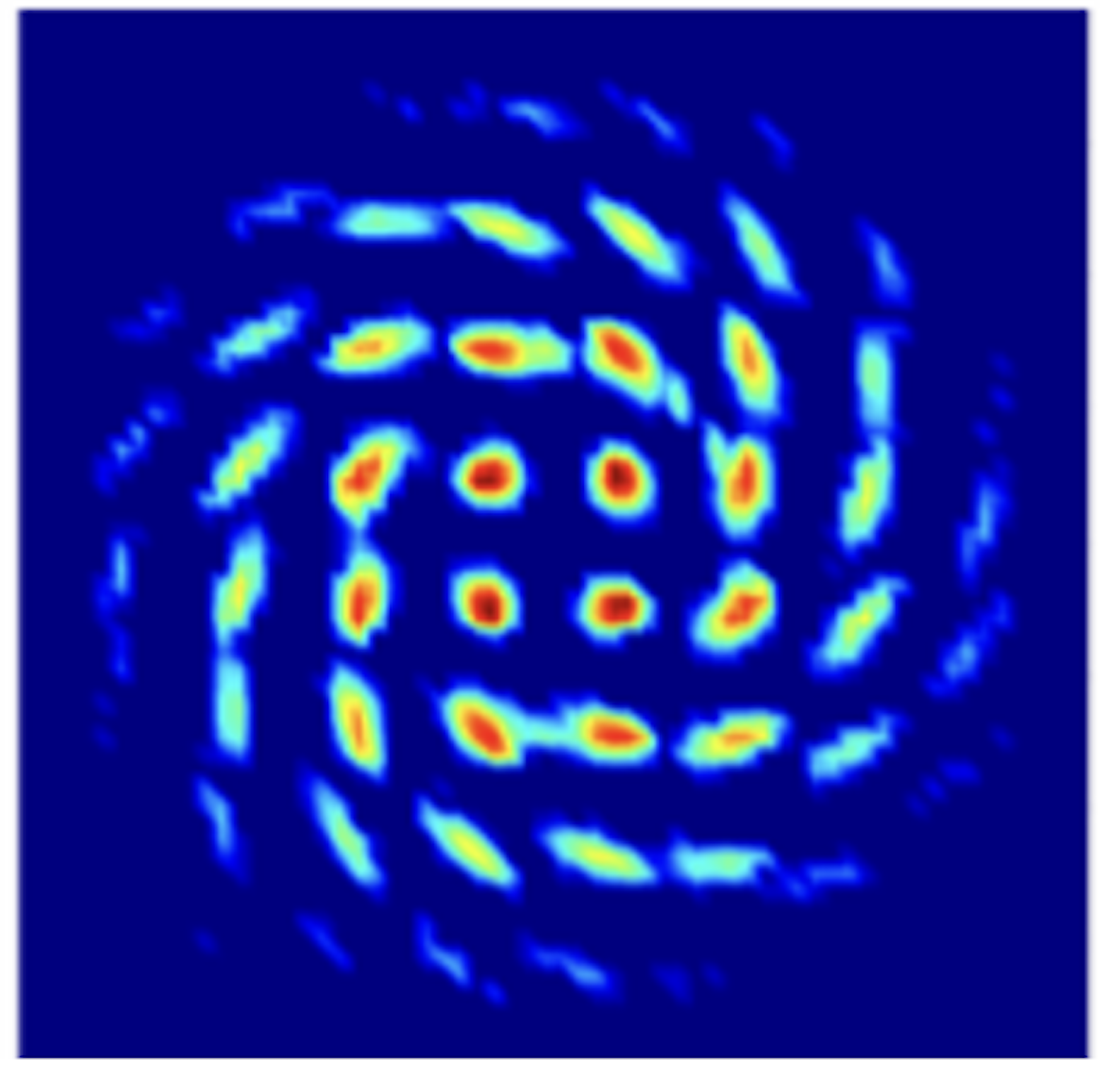
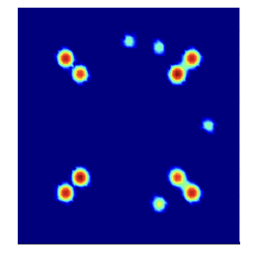
Such curtailing of the driver saves power but results in ‘modulator loss’; the area occupied by the modulator’s constellation points is less than the ideal available (see top left diagram).
“You not driving the modulator to the limit,” says Tomkos. “Modulation loss can be as high as 9-12dB which impacts signal recovery at the receiver.”
The relation between the driving DAC inputs and the discrete optical outputs is generally nonlinear (see diagram above). This means the constellation points look warped and are not spaced equally apart causing signal distortion.
Such optical distortion can be tackled using various specialised DAC architectures but the cost is either higher power, limited speed or extra modulation loss.
“Ideally, we would like to have equal distances between the symbols so we can robustly separate each symbol from the others since we also have electronic errors coming from the DACs that impact the quality of the symbols and shift them from their optimal points,” says Tomkos.
The impact of modulation loss and optical distortion also worsen when higher modulation schemes above 16-QAM are used.
The oDAC
Mention the term optical DAC, and specific thoughts come to mind. Is the optical signal sampled? Is the DAC electrical in its input and output, but its inner workings are photonic?
The optical DAC, as proposed by Nazarathy and Tomkos, is neither of the above. Moreover, it uses existing driver electronics based on the simplest traditional lowest-order DACs.
Indeed, the oDAC looks similar to a conventional coherent optics transmitter in terms of components, but the differences in operation and achieved performance are significant.
The oDAC can also be implemented in several ways bringing critical benefits for various system requirements.
Architecture
A conventional coherent optical transmitter splits the incoming laser source and feeds the light equally to the in-phase and quadrature Mach-Zehnder modulators (one arm of which includes a 90-degree phase shifter).

The two Mach-Zehnder modulators are driven, as shown. In this example, two drivers implement a bipolar 4-level pulse amplitude modulation (PAM-4) signal such that the coherent transmitter produces a 16-QAM output signal.
The oDAC architecture is subtly different.
The oDAC’s main two components are a variable splitter and combiner at the input and output and the Mach-Zehnder modulator pair. Here, both modulators are identical; there is no 90o phase shifter but the differential phase is maintained at 0o degrees and the modulators are operated at full-scale resulting in zero modulation loss (see diagram at the article’s start).

Each modulator arm is driven by an electrical PAM-4 signal, and the variable splitter-combiner produces the bipolar PAM-16 optical output.
For 16-PAM, 4/5 of the laser signal is fed to one arm and the remaining 1/5 to the other. The PAM-4 DAC drivers for both Mach-Zehnder modulators are identical.
“In the first case, we had 16 symbols in two dimensions (i.e. QAM16); here we have 16 symbols, but in one dimension (i.e. PAM16), the other dimension is missing due to the absence of the 90-degree phase shifter,” says Tomkos.
According to Tomkos, the sine nonlinearity of the optical modulators here is an advantage. “The generated signal does not suffer from modulation loss and optical distortion due to electronic driver mismatch errors, as the noise coming from the electronic DACs gets squelched,” he says.
Higher-order modulation
As mentioned, the oDACs can be implemented and arranged in several ways.
For example, two oDACs can be used, one orthogonal in phase to the other, in a conventional coherent transmitter structure to generate a higher modulation signal. For example, two optical DAC arms, each 16-PAM, used as I and Q, will produce a 256-QAM signal.
But even more strikingly, more than two parallel modulation paths (by stacking-up more modulators in parallel, see diagram) can be used as an alternative approach to generating higher-order modulation schemes and higher bit rates, and at reduced power consumption per bit.
“The ratio between the bit rate and the baud rate is exactly the number of parallel paths,” says Nazarathy. “Another name for it is spectral efficiency: how many bits each symbol carries.”
The oDAC uses straightforward drivers. The professors say only PAM-2 or PAM-4 drivers are used. This way, power savings are maximised.
“The big picture is that we offload the electronics burden by going parallel optically,” says Nazarathy, adding that what is being traded is electronic DAC complexity and the associated performance limitations of the drivers for optical parallelism of replicated blocks of Mach-Zehnder modulators.
“You don’t want to stack things [photonic componentry] serially as if you keep stacking that way, you incur an optical loss because the loss is compounded,” says Nazarathy. Here, the modulators are stacked in parallel, the preferred integration approach.
Moreover, the more paths used, the higher-order the generated optical constellation is. “Eventually, only PAM-2 (Non-return-to-zero) drivers are used and that’s the minimum power consumption you can get,” says Tomkos.
“So we have parallelism (at the same laser power) that generates for the same baud rate, double or triple the bit rate [depending on whether 2 or 3 paths are used],” says Nazarathy. And the resulting constellations are near ideal: there is no modulation loss, nor is there optical distortion.
Nazarathy explains such benefits as the result of a ‘divide-and-conquer’ approach.
“If you keep the modulation paths simple, you have more freedom to optimise the drive point of the modulators,” he says. “The modulators benefit you more because they are more simply driven.” Then, by adding more modulator paths, the system performance improves overall.”
He also notes how the optical implementation is robust to imperfections generated by the electronic circuitry.
Optical DAC: A definition
- Two or more optical modulator units and some static or slowly-tuned ‘glue’ optics.
- The electrical drivers feeding the optical modulators are simple for lowest-power, either PAM2 (NRZ) or PAM4 drivers. Electronic DACs generating higher-order PAM are not needed.
- No high-speed power-hungry digital encoder (mapper) is used. The number of Mach-Zehnder modulators is B where the constellation size is C=2B. This is referred to as Direct Digital Drive. This last condition ensures the lowest power consumption.
Status
The oDAC work is currently at the research stage.
The working of the oDAC has been simulated and verified, and several papers have been published. Patents have also been filed.
At the recent OFC event in San Diago in March, Professor Tomkos met with hyperscalers, systems and components vendors to explain the oDAC technology and its benefits.
The two academics are focused on the oDAC in the optical transmitter, but Nazarathy says they also plan to surprise at the optical receiver end.
Tomkos says the optical DAC is an ideal fit for future coherent transmitters that will be used in 6G networks and datacenter networks, which will carry significant amounts of traffic at ultra-high rates.
The oDAC approach also bodes well for the trend of using linear drive optics. Indeed, the implementation of the oDAC hardware is carried out within the framework of a major R&D project called FLEX-SCALE that Tomkos is co-ordinating and is funded under the first phase of the 6G Smart Networks and Services (SNS) Partnership.
Tomkos believes that the first use of the optical DAC may likely be for data centre interconnect, a more mature market where higher-order modulation formats can be used and low-power is at a premium.
The professors are looking for partners and exploring options to commercialise the technology.
Nokia jumps a class with its PSE-6s coherent modem
- The 130 gigabaud (GBd) PSE-6s coherent modem is Nokia’s first in-house design for high-end optical transport systems
- The PSE-6s can send an 800 gigabit Ethernet (800GbE) payload over 2,000km and 1.2 terabits of data over 100km.
- Two PSE-6s DSPs can send three 800GbE signals over two 1.2-terabit wavelengths
Nokia has unveiled its latest coherent modem, the super coherent Photonic Service Engine 6s (PSE-6s) that will power its optical transport platforms in the coming years.
The PSE-6s comes three years after Nokia announced its current generation of coherent digital signal processors (DSPs): the PSE-Vs DSP for the long-haul and the compact PSE-Vc for the coherent pluggable market.
Nokia is only detailing the PSE-6s; its next-generation coherent modem for pluggables will be a future announcement.
Nokia will demonstrate the PSE-6s at the upcoming OFC show in March while field trials involving systems using the PSE-6s will start in the year’s second half.
Reducing cost per bit
In 2020, Nokia bought Elenion, a silicon photonics company specialising in coherent optics.
The PSE-6s is Nokia’s first in-house coherent modem – the coherent DSP and associated optics – targeting the most demanding optical transport applications.
Nokia points out that coherent systems started approaching the Shannon limit two generations ago.
In the past, operators could reduce the cost of optical transport by sending more data down a fibre; upgrading the optical signal from 100 to 200 to 400 gigabit required only a 50GHz channel.
“You were getting more fibre capacity with each generation,” says Serge Melle, director of product marketing, optical networks at Nokia. And this helped the continual reduction of the cost-per-bit metric.
But with more advanced DSPs, implemented using 16nm, 7nm, and now 5nm CMOS, going to a higher symbol rate and hence data rate requires more spectrum, says Melle.
Increasing the symbol rate is still beneficial. It allows more data to be sent using the same modulation scheme or transmitting the same data payload over longer distances.
“So one of the things we are looking to do with the PSE-6s is how do we still enable a lower total cost of ownership even though you don’t get more capacity per wavelength or fibre,” says Melle.

Symbol rate classes
Coherent optics from the leading vendors use a symbol rate of 90-107 gigabaud (GBd), while Cisco-owned Acacia’s latest 1.2-terabit coherent modem in a CIM-8 module operates at 140GBd.
Acacia uses a classification system based on symbol rate. First-generation coherent systems operating at 30-34GBd are deemed Class 1. Class 2 doubles the baud rates to 60-68GBd, the symbol rate window used for 400ZR coherent optics, for hyperscalers to connect equipment across their data centres up to 120km apart.
The DSPs from the leading optical transport systems vendors operating at 90-107GBd are an intermediate step between Class 2 and Class 3 using Acacia’s classification. In contrast, Acacia has jumped directly from Class 2 to Class 3 with its 140GBd CIM-8 coherent modem.
Competitors view Acacia’s classification scheme as a marketing exercise and counter that their 90-107GBd optical transport systems benefited customers for over two years.
Nokia’s 90GBd PSE-Vs can send 400 gigabits using quadrature phase-shift keying (QPSK) over 3,000km. This contrasts with its earlier 67GBd PSE-3s that sends 400GbE up to 1,000km using 16-QAM.
However, with the PSE-Vs, Nokia, unlike its optical transport competitors, Infinera, Ciena and Huawei, decided not to support 800-gigabit wavelengths.
Nokia argued that 7nm CMOS, 90-100GBd coherent optics tops out at 600 gigabit when used for distances of several hundred kilometers, while metro-regional distances are more economically served using 400-gigabit pluggable optics such as the CFP2 implementing 400ZR+.
With the 130Gbd PSE-6s, Nokia has a Class 3 coherent modem with the PSE-6s capable of sending 800 gigabits more than 2,000km.
The PSE-6s also doubles the maximum data rate of the PSE-Vs to 1.2 terabits per wavelength. However, at 1.2 terabits, the reach is 100-plus km, valuable for very high capacity metro transport and data centre interconnect.
Scale, reach and power consumption per bit
Nokia highlights the PSE-6s’ main three performance metric improvements.
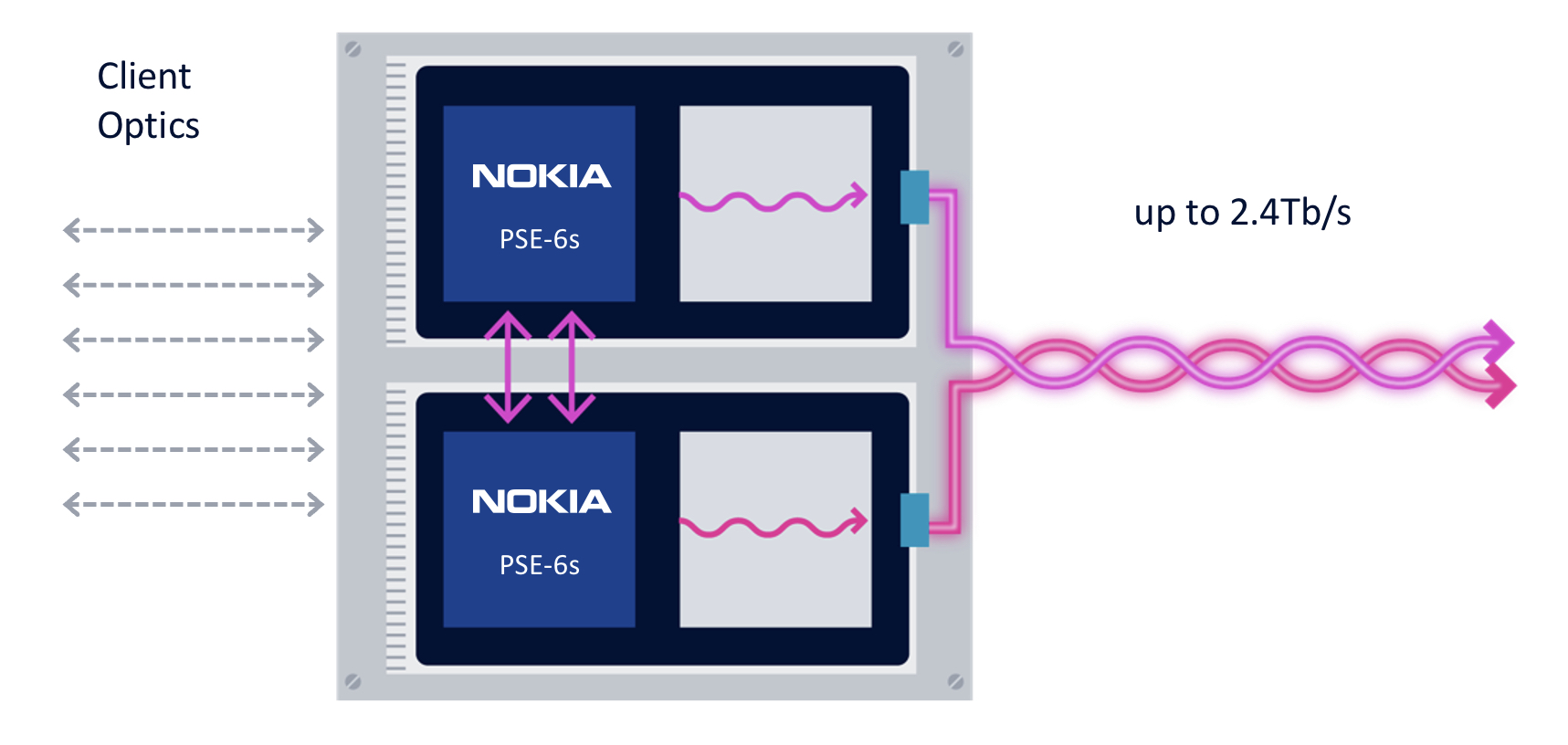
First, the coherent modem delivers scaling: two coherent optical engines fit on a line card to deliver 2.4 terabits to transport emerging high-speed services such as 800GbE.
The two PSE-6s are linked using a dedicated interface to share the client-side signals (see diagram).
“We are not the only ones introducing a 5nm solution, but I think we are the only ones that allow two DSPs to work together,” says Melle.
Without the interface, a single 800GbE and up to four 100GbE clients or a 400GbE client can be sent over each DSP’s 1.2-terabit wavelength. Adding the interface, an operator can send three uniform 800GbE clients, with the interface splitting the third 800GbE client between the two DSPs.
“In a single line card, you can stripe the three 800-gigabit services rather than have to deploy three separate line cards in the network,” says Melle.
Nokia is not detailing the interface used to link the DSPs but said that the interface is used for data only and not to share signal processing resources between the ASICs.
“There is an extra amount of circuitry to share the client bandwidth across the two DSPs, but it is not high power consuming, and most transponders have some circuitry between the clients and the DSP,” says Melle. “So the incremental ‘power tax’ is marginal; it doesn’t add any significant power overhead.”
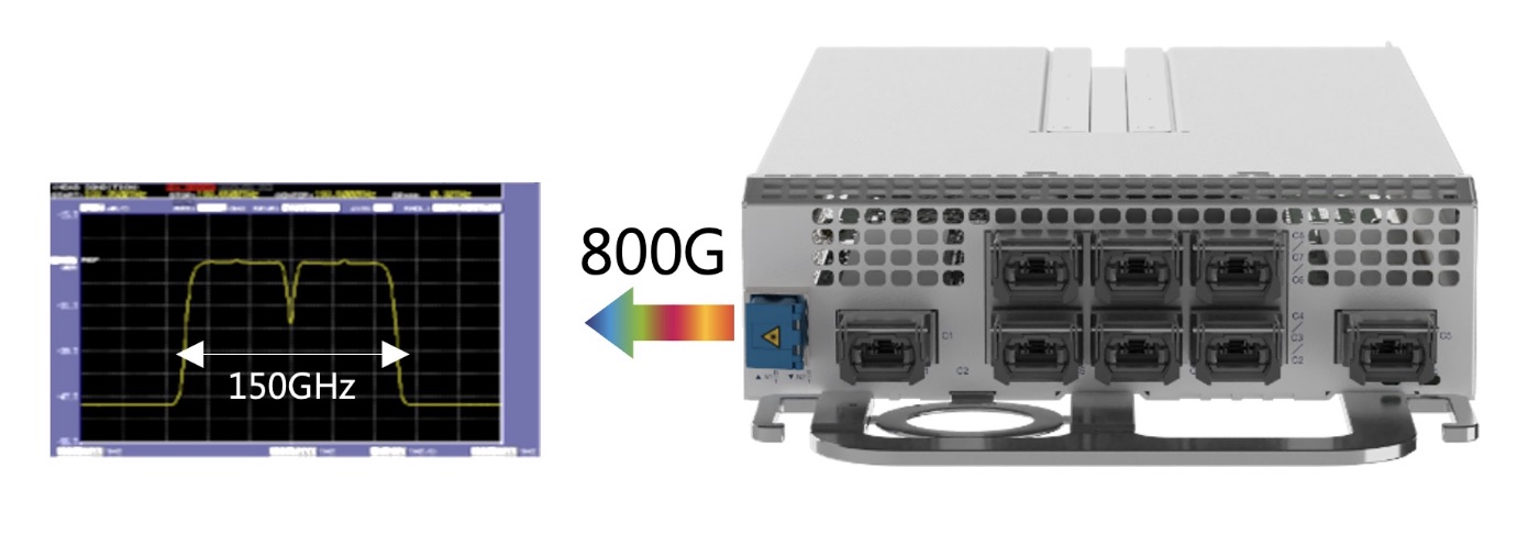
The resulting 2.4-terabit transmission is sent as two 1.2-terabit wavelengths, each occupying a 150GHz-wide channel. Existing systems that operate at 90-107GBd typically use a 112.5GHz channel for an 800-gigabit transmission, so the PSE-6s delivers a fibre capacity benefit.
The two wavelengths can be bonded, as in a two-channel ‘super-channel’, or sent to separate locations.
The second improvement is optical performance. For example, an 800-gigabit payload can travel over 2,000km. Nokia claims this is 3x the reach of existing commercial optical transport systems.
The improved transmission performance is achieved using a combination of the 130GBd baud rate, probabilistic constellation shaping (PCS), and improved forward error correction (FEC). Melle says the contributions to the improvement are 90 per cent baud rate and 10 per cent due to coherent modem algorithm tweaks.
“Baud rate is king; that is what really drives this improved performance,” says Melle.
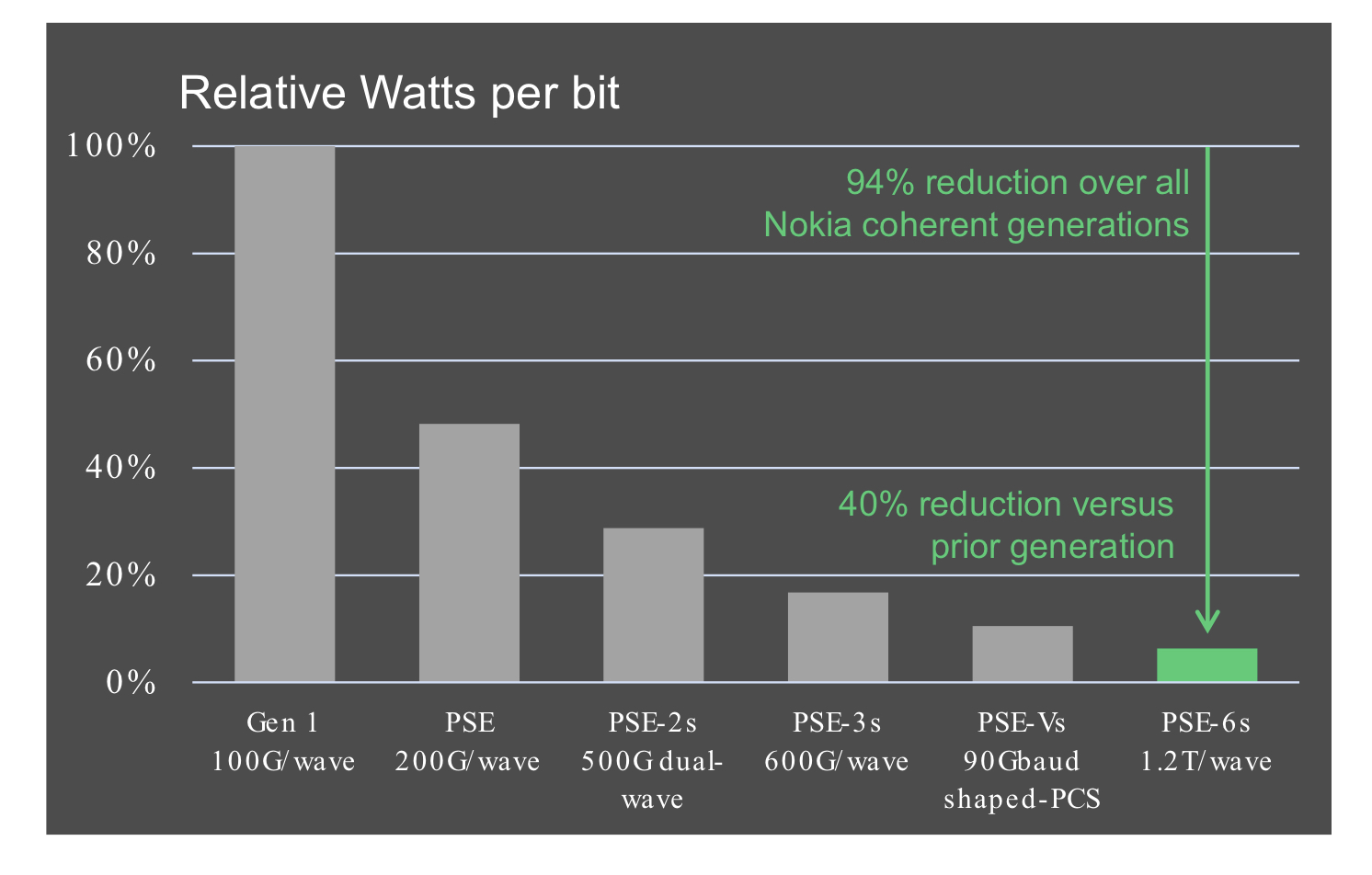
The third benefit is reduced power consumption at the device and system (networking) levels.
Using a 5nm finFET CMOS process to make the PSE-6s DSP ASIC and developing denser line cards (two modems per card) means systems will consume 60 per cent less power than Nokia’s existing coherent technology.
According to Nokia, the PSE-6s optical engine consumes 40 per cent fewer Watts per bit compared to the PSE-Vs.
Nokia 1830 transport systems
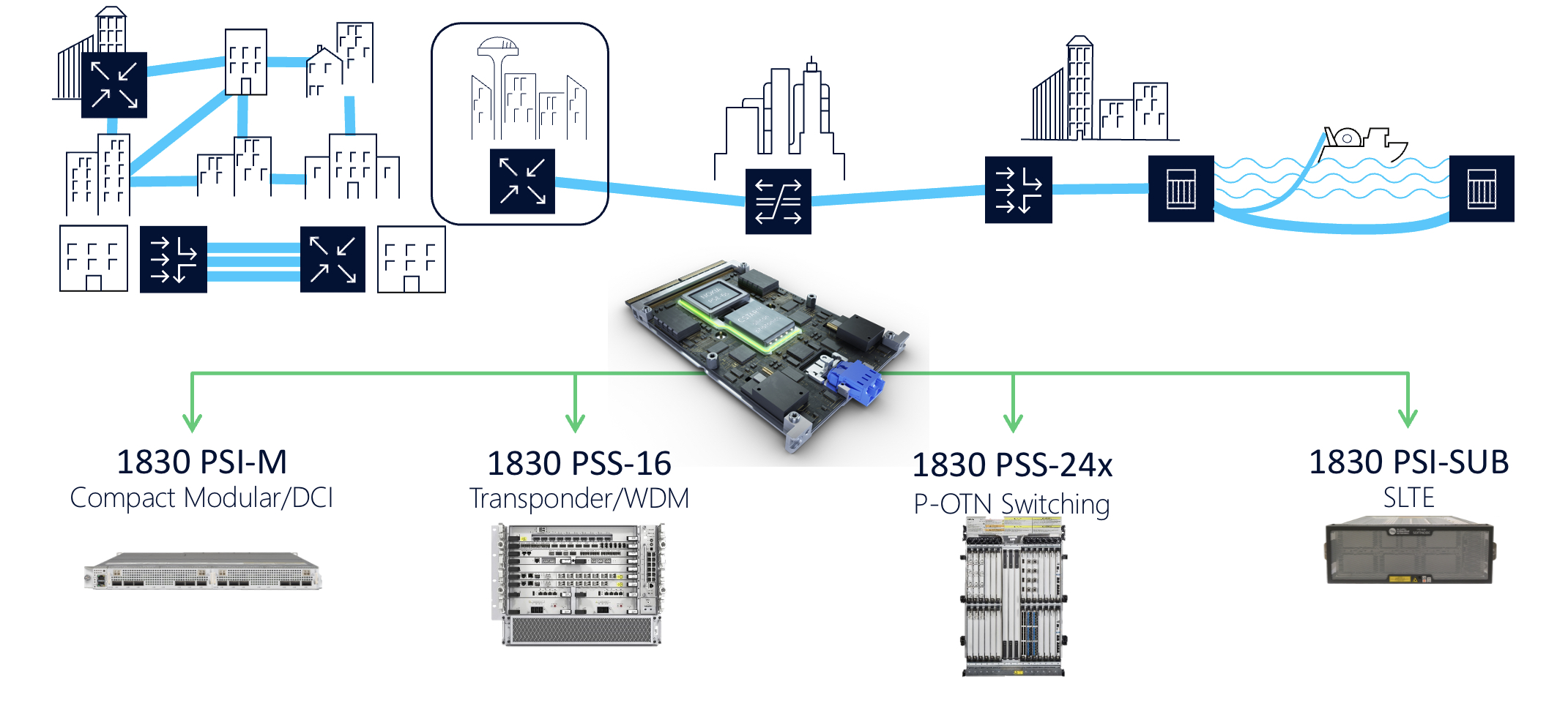
The PSE-6s line cards fit into Nokia’s existing range of 1830 transport platforms.
These include the 1830 PSI-M compact modular data centre interconnect, the 1830 PSS-16 transponder and WDM line system, the 1830 PSS-24x P-OTN and switching chassis, and the 1830 PSI-SUB subsea line-terminating equipment.
For example, the PSI-M platform can hold two line cards, each with two PSE-6s.

Effect Photonics buys the coherent DSP team of Viasat

Effect Photonics has completed the acquisition of Viasat’s staff specialising in coherent digital signal processing and forward error correction (FEC) technologies and the associated intellectual property.
The company also announced a deal with Jabil Photonics – a business unit of manufacturing services firm Jabil – to co-develop coherent optical modules that the two companies will sell.
The deals enable Effect Photonics to combine Viasat’s coherent IP with its indium phosphide laser and photonic integrated circuit (PIC) expertise to build coherent optical designs and bring them to market.
Strategy
Harald Graber, chief commercial officer at Effect Photonics, says the company chose to target the coherent market after an internal strategic review about how best to use its PIC technology.
The company’s goal is to make coherent technology as affordable as possible to address existing and emerging markets.
“We have a kind of semiconductor play,” says Graber. By which he means high-volume manufacturing to make the technology accessible.
“When you go to low cost, you cannot depend 100 per cent on buying the coherent digital signal processor (DSP) from the merchant market,” he says. “So the idea was relatively early-born that somehow we had to address this topic.”
This led to talks with Viasat and the acquisition of its team and technology.
Markets
“We also saw, as with some of our competitors, that making modules for satellite or free-space optics has a natural harmony for the roadmaps,” says Graber.
Effect Photonics and Jabil Photonics will bring to market an advanced, low-power coherent module design based on the QSFP-DD form factor.
Graber says 400ZR+ coherent modules fall short in their output power which is noticeable for networks with multiple reconfigurable optical add/drop multiplexing (ROADM) stages.
“So you need a little more [output power], and our technology allows us to do more,” he says.
By owning a coherent DSP and PIC, the company can integrate closely the two to optimise the coherent engine’s optical performance.
“You have a lot of room for improvement, which you cannot do when you buy a merchant DSP, especially when we talk about a 1.6 terabit design and above,” says Graber. “Our optical machine is already fully integrated, including the laser. It’s just now this last piece part to alleviate the current industry barriers.”
Effect Photonics’ focus is the communications sector. “We are putting everything in place to serve the hyperscalers,” says Graber.
The company is also looking at satellite communications and free-space optics.
Effect Photonics is working with Aircision, a company developing a free-space optics system that can send 10 gigabit-per-second (Gbps) over a 5km link for mobile backhaul and broadband applications.
Having all the parts for coherent designs will enable the company to address other markets like quantum key distribution (QKD) and lidar.
“The main problem with QKD is you cannot use amplification,” says Graber. “You need to have something fully integrated, with a nice output power to achieve the links.”
Graber says that for QKD, the company will only have to tweak its chip.
“We just have to make sure that the internal noise is in the right levels and these kinds of things,” says Graber. “So there’s a lot of opportunities; it puts us in a nice position.”
Company
Effect Photonics is headquartered in The Netherlands and has offices in four countries.
Last year, the company raised $43M in Series-C funding. The company raised a further $20 million with the Viasat deal.
The company has 250 staff, split between engineering and a large manufacturing facility.

Huawei sets transmission record with new modulator

Coherent discourse: Part 1
A paper from Huawei and Sun Yat-Sen University in the January issue of the Optica journal describes a thin-film lithium niobate modulator. The modulator enabled a world-record coherent optical transmission, sending nearly 2 terabits of data over a single wavelength.
Much of the industry’s focus in recent years has been to fit coherent optical technology within a pluggable module.
Such pluggables allow 400-gigabit coherent interfaces to be added to IP routers and switches, serving the needs of the data centre operators and telecom operators.
But research labs of the leading optical transport vendors continue to advance high-end coherent systems beyond 800-gigabit-per-wavelength transmissions.
Optical transport systems from Ciena, Infinera and Huawei can send 800-gigabit wavelengths using a symbol rate of 96-100 gigabaud (GBd).
Acacia Communications, part of Cisco, detailed late last year the first 1.2-terabit single-wavelength coherent pluggable transceiver that will operate at 140GBd, twice the symbol rate of 400-gigabit modules such as 400ZR.
Now Huawei has demonstrated in the lab a thin-film lithium niobate modulator that supports a symbol rate of 220GBd and beyond.
Maxim Kuschnerov, director of the optical and quantum communications laboratory at Huawei, says the modulator has a 110GHz 3dB bandwidth but that it can be operated at higher frequencies, suggesting a symbol rate as high as 240GBd.
Thin-film lithium niobate modulator
Huawei says research is taking place into new materials besides the established materials of indium phosphide and silicon photonics. “It is a very exciting topic lately,” says Kuschnerov.
He views the demonstrated thin-film lithium niobate optical modulator as disruptive: “It can cover up several deficiencies of today’s modulators.”
Besides the substantial increase in bandwidth – the objective of any new coherent technology – the modulator has performance metrics that benefit the coherent system such as a low driving voltage and low insertion loss.
A driving voltage of a modulator is a key performance parameter. For the modulator, it is sub-1V.
The signal driving the modulator comes from a digital-to-analogue (D/A) converter, part of the coherent digital signal processor (DSP). The D/A output is fed into a modulator driver. “That [driver] requires power, footprint, and increases the complexity of integrating the [modem’s] modules tighter,” says Kuschnerov.
The modulator’s sub-1V drive voltage is sufficiently small that the DSP’s CMOS-based D/A can drive it directly, removing the modulator driver circuit that also has bandwidth performance limitations. The modulator thus reduces the transmitter’s overall cost.
The low-loss modulator also improves the overall optical link budget. And for certain applications, it could even make the difference as to whether optical amplification is needed.
“The modulator checks the box of very high bandwidth,” says Kuschnerov. “And it helps by not having to add a semiconductor optical amplifier for some applications, nor needing a driver amplifier.”
One issue with the thin-film modulator is its relative size. While not large – it has a length of 23.5mm – it is larger than indium phosphide and silicon photonics modulators.
1.96-terabit wavelength
Huawei’s lab set-up used a transmit coherent DSP with D/As operating at 130 Giga-samples-per-second (GS/s) to drive the modulator. The modulation used was a 400-quadrature amplitude modulation (400-QAM) constellation coupled with probabilistic constellation shaping.
A 10 per cent forward error correction scheme was used such that, overall, 1.96-terabits per second of data was sent using a single wavelength.
The D/A converter was implemented in silicon germanium using high-end lab equipment to generate the signal at 130GS/s.
“This experiment shows how much we still need to go,” says Kuschnerov. “What we have done at 130GBd shows there is a clear limitation with the D/A [compared to the 220GBd modulator].”
Baud-rate benefits
Increasing the baud rate of systems is not the only approach but is the favoured implementation choice.
What customers want is more capacity and reducing the cost per bit for the same power consumption. Increasing the baud rate decreases the cost and power consumption of the optical transceiver.
By doubling the baud rate, an optical transceiver delivers twice the capacity for a given modulation scheme. The cost per bit of the transceiver decreases as does the power consumed per bit. Instead of two transceivers and two sets of components, one transceiver and one set are used instead.
But doubling the baud rate doesn’t improve the optical system’s spectral efficiency since doubling the baud rate doubles the channel width. That said, algorithmic enhancements are added to each new generation of coherent modem but technically, the spectral efficiency practically no longer improves.
Huawei acknowledges that while the modulator promises many benefits, all the coherent modem’s components – the coherent ASIC, the D/A and analogue-to-digital (D/A) converters, the optics, and the analogue circuitry – must equally scale. This represents a significant challenge.
Kuschnerov says optical research is finding disruptive answers but scaling performance, especially on the electrical side, remains a critical issue. “How do you increase the D/A sampling rates to match these kinds of modulator technologies?” he says. “It is not straightforward.”
The same is true for the other electrical components: the driver technologies and the trans-impedance amplifier circuits at the receiver.
Another issue is combining the electrical and optical components into a working system. Doubling the signalling of today’s optical systems is a huge radio frequency design and packaging challenge.
But the industry consensus is that with newer CMOS processes and development in components and materials, doubling the symbol rate again to 240GB will be possible.
But companies don’t know – at least they are not saying – what the upper symbol rate limit will be. The consensus is that increasing the baud rate will end. Then, other approaches will be pursued.
Kuschnerov notes that if a 1.6-terabit transceiver could be implemented using a single wavelength or with eight 200Gbps ones with the same spectral performance, cost, footprint and power consumption, end users wouldn’t care which of the two were used.
However, does optics enable such greater parallelism?
Kuschnerov says that while decades of investment has gone into silicon photonics, it is still not there yet.
“It doesn’t have the cost-effectiveness at 16, 32 or 64 lanes because the yield goes down significantly,” he says. “We as an industry can’t do it yet.”
He is confident that, soon enough, the industry will figure out how to scale the optics: “With each generation, we are getting better at it.”
Coherent engineers will then have more design options to meet the system objectives.
And just like with microprocessors, it will no longer be upping the clock frequency but rather adopting parallel processing i.e. multiple cores. Except, in this case, it will be parallel coherent optics.

ADVA’s 800-gigabit CoreChannel causes a stir

ADVA’s latest addition to its FSP 3000 TeraFlex platform provides 800-gigabit optical transmission. But the announcement has caused a kerfuffle among its optical transport rivals.
ADVA’s TeraFlex platform supports various coherent optical transport sleds, a sled being a pluggable modular unit that customises a platform’s functionality.
The coherent sleds use Cisco’s (formerly Acacia Communication’s) AC1200 optical engine. Cisco completed the acquisition of Acacia in March.
The AC1200 comprises a 16nm CMOS Pico coherent digital signal processor (DSP) that supports two wavelengths, each up to 600-gigabit, and two photonic integrated circuits (PICs), for a maximum capacity of 1.2 terabits.
The latest sled from ADVA, dubbed CoreChannel, supports an 800-gigabit stream in a single channel.
ADVA states in its press release that the CoreChannel uses “140 gigabaud (GBd) sub-carrier technology” to deliver 800-gigabit over distances exceeding 1,600km.
This, the company says, improves reach by over 50 per cent compared with state-of-the-art 95GBd symbol rate coherent technologies.
It is these claims that have its rivals reacting.
“Despite their claims – they are not using actual digital sub-carriers,” says one executive from a rival optical transport firm, adding that what ADVA is doing is banding two independent 70GBd 400-gigabit wavelengths together and trying to treat that as a single 800-gigabit signal.
“This isn’t necessarily a bad solution for some applications – each network operator can decide that for themselves,” says the executive. However, he stresses that the CoreChannel is not an 800-gigabit single-channel solution and uses 4th generation 16nm CMOS DSP technology rather than the latest 5th generation, 7nm CMOS DSP technology.
A second executive, from another optical transport vendor providing 800-gigabit single-wavelength solutions, adds that ADVA’s claim of 140GBd is too ‘creative’ for a two-lambda solution.
“It’s not a real 800 gigabit. Not that this must be bad, but one should call things as they are,” the spokesperson said. “What matters to the operators is the cost, power consumption, reach and density of a modem; the number of lambdas is more of an internal feature.”
CoreChannel
ADVA confirms it is indeed using Cisco’s Pico coherent DSP to drive two wavelengths, each at 400 gigabits-per-second (Gbps).
“You can say the CoreChannel is a less challenging requirement because we are not driving it [the Pico DSP] to the maximum modulation or constellation complexity,” says Stephan Rettenberger, senior vice president, marketing and investor relations at ADVA. “It is the lower end of what the AC1200 can do.”
Until now the two wavelengths have been combined externally, and have not been integrated from a software or a command-and-control approach.
“The CoreChannel sled is just another addition to the TeraFlex toolbox,” says Rettenberger. “It has one physical line interface that drives an 800Gbps stream using two wavelengths, each one around 70GBd, that are logically and physically combined.”
The resulting two-wavelength 800-gigabit stream sits within a 150GHz channel. However, the channel width can be reduced to 125GHz and even 112.5GHz for greater spectral efficiency.
ADVA says the motivation for the design is the customers’ requirement for lower-cost transport and the ability to easily transport 400 Gigabit Ethernet (GbE) client signals.
“With this 800-gigabit line speed, you can go something like 2,000km, that is 50-100 per cent more than what 95GBd single-wavelengths solutions will do,“ says Rettenberger. “And you can also drive it at 400 gigabits and you can do something like 6,000km.”
The reaches quoted are based on a recent field trial involving ADVA.
ADVA uses a single DSP, similar to the latest 800-gigabit systems from Ciena, Huawei and Infinera. Alongside the DSP are two non-hermetically-sealed PICs whereas the 95GBd indium-phosphide solutions use a single hermetically sealed gold box.
ADVA’s solution also requires two lasers whereas the 800-gigabit single-wavelength solutions use one laser.
“Yes, we have two lasers versus one but that is not killing the cost,” says Rettenberger. “And it is also not killing the power consumption because the PIC is so much more power efficient.”
Rettenberger stresses that ADVA is not saying its offering is necessarily a better solution. “But it is a very interesting way to drive 800 gigabits further than these 95 gigabaud solutions,” says Rettenberger. “It has the same cost, space, power efficiency, just greater reach.”
ADVA also agrees that it is not using electrical sub-carriers such as Infinera uses but it is using optical sub-carrier technology.
These two wavelengths are combined logically and also from a physical port interface point of view to fit within a 150GHz window.
The 95GBd, in contrast, is an interim symbol rate step and the resulting 112.5GHz channel width doesn’t easily fit with legacy 25GHz and 50GHz band increments, says ADVA, while the 150GHz band the CoreChannel sled uses is the same channel width that will be used once single-wavelength 140GBd technology becomes available.
Acacia has also long talked about the merit of doubling the baud rate suggesting Cisco’s successor to the AC1200 will have a 140GBd symbol rate. Such a design is expected in the next year or two.
“We feel this [CoreChannel] implementation is already future-proofed,” says Rettenberger.
ADVA says it undertook this development in collaboration with Acacia.
Acacia announced a dual-wavelength single-channel AC1200 solution in 2019. Then, the company unveiled its AC1200-SC2 that delivers 1.2 terabits over an optical channel.
The SC2 (single chip, single channel) is an upgrade of Acacia’s AC1200 module in that it sends 1.2 terabits using two sub-carriers that fit in a 150GHz-wide channel.

Customer considerations
Choosing an optical solution comes down to five factors, each having its weight depending on the network application, says the first executive.
These are capacity-per-wavelength, cost-per-bit, capacity-per- optical-engine or -module, spectral efficiency and hence capacity-per-fibre, and power-per-bit.
“Each is measured for a given distance/ network application,” says the executive. “And the reason the weight changes for different applications is that the importance of each factor is different at different points in the network. For example, the importance of spectral efficiency changes depending on how expensive it is to light up a link (fibre and line system costs).”
For long-haul and submarine, spectral efficiency is the most important factor, while for metro it is typically cost-per-bit. Meanwhile, for data centre interconnect applications, it’s a mix between cost-per-bit and power-per-bit. Capacity-per-wave and capacity-per-optical-engine are valuable because they can reduce the number of wavelengths and modules that need to be deployed, reducing operating expenses and accelerating service activation.
“The reason that 5th generation [7nm CMOS technology] is superior to fourth generation [16nm] DSP technology is that it provides superior performance in every single one of those key criteria,” says the executive. “This fact minimised any potential benefits that could be achieved by banding together two wavelengths using 4th generation technology when compared to a single wavelength using 5th generation technology.”
“It sounds like others feel we have misled the market; that was not the intent,” says Rettenberger.
ADVA does not make its own coherent DSP so it doesn’t care if the chip is implemented using a 16nm, 7nm or a 5nm CMOS process.
“We are trying to build a good solution for transmitting 400GbE signals and, for us, the Pico chip is a wonderful piece of technology that we have now implemented in four different [sled] variants of TeraFlex.”