
Marvell’s CTO: peering into the future is getting harder
CTO interviews part 4: Noam Mizrahi
In a wide-ranging interview, Noam Mizrahi (pictured), executive vice president and corporate chief technology officer (CTO) at Marvell, discusses the many technologies needed to succeed in the data centre. He also discusses a CTO’s role and the importance of his focussed thinking ritual.
Noam Mizrahi has found his calling.
“I’m inspired by technology,” he says. “Every time I see an elegant technical solution – and it can be very simple – it makes me smile.”
Marvell hosts an innovation contest, and at one event, Mizrahi mentioned this to participants. “So they issued stickers saying, ‘I made Noam smile’,” he says.
Marvell’s broad portfolio of products spans high-end processors, automotive Ethernet, storage, and optical modules.
“This technology richness means that every day I come to work, I feel I learn something new,” he says.
Chip design
The interview with Mizrahi occurred before the passing away on March 24th of Gordon Moore, aged 94, who co-founded Intel.
In his article published in Electronics in 1965, Moore observed how chip transistor count doubled roughly yearly, what became known as Moore’s law.
The law has driven the semiconductor industry for decades and, like all exponential trends, is reaching its limit.
Since Marvell’s business is infrastructure ICs, it is experiencing the law’s demise first hand.
While the core definition of Moore’s law is ending, technology and process advancement are still enabling the cramming of more transistors on a die, says Mizrahi. However, greater processing performance and lower power consumption are occurring at a different pace and cost structure.
It is now very costly to make chips using the latest 5nm and 3nm CMOS process nodes.
The cost is not just the chip mask (reticle) but also such aspects as intellectual property (IP), architecture, design verification, electronics design automation (EDA) tools, and design validation.
Getting to the first product using 5nm CMOS can cost as high as $450 million, while for 3nm, the estimate is $600 million.
Also, development flow takes longer due to the complexity involved and will cause a redefinition of what is meant by a ‘current generation’ of a chip, says Mizrahi.
Design reuse is also increasingly required; not just reusing IP but the validation process in order to speed up a chip’s introduction.
In turn, designers must be innovative since processing performance and lower power consumption are harder to achieve.
Areas include package design optimisation, chip input-output (I/O), and the software to claw back processing performance that previously came from using the latest CMOS process.
IC designers will also be forced to choose which chips to make using the latest CMOS process node.
Overall, fewer chip companies will be able to afford chips made in leading CMOS processes, and fewer companies will buy such ICs, says Mizrahi.
Rise of chiplets
Chiplets will also play a role in a post-Moore’s law world.
“Chiplets are currently a very hot topic,” says Mizrahi.

A chiplet is a die implementing a functional block. The chiplet is added alongside a central die for a system-on-chip (SoC) design. Using chiplets, designs can exceed the theoretical limit of the mask size used to make a chip.
Marvell has long been a chiplet pioneer, says Mizrahi. “Today, it all seems reasonable, but when we did all that, it was not so obvious.” Marvell makes one chip that has 17 dies in a package.
Chiplets are particularly suited for artificial intelligence (AI) ASICs, what Mizrahi describes as ‘monsters of chips’.
Chiplets enable designers to control yield, which is essential when each 3nm CMOS chip lost to a defect is so costly.
Using chiplets, a design can be made using a mix of CMOS process nodes, saving power and speeding up a chip’s release.
Mizrahi applauds the work of the Universal Chiplet Interconnect Express (UCIe) organisation, creating chiplet standards.
But the chiplets’ first use will be as internally-designed dies for a company’s product, he says. Chip designers buying best-in-class chiplets from third parties remains some way off.
A CTO’s role
Mizrahi’s role is to peer into the future to identify the direction technologies will take and their impact on Marvell’s markets and customers.
He says a company-level longer-term technological strategy that combines the strengths of Marvell’s product lines is needed to secure the company’s technical lead.
“That is my job, and I love it,” he says.
It’s also challenging; predicting the future is hard, especially when the marketplace is dynamic and constantly changing. Technology is also very costly and time-consuming to develop.
“So, making the right decision as to what technology we need to invest in for the future, that is tough,” says Mizrahi.
Rapidly changing market dynamics are also challenging Marvell’s customers, who don’t always know what they need to do.
“Creating this clarity with them is challenging but also a great opportunity if done correctly,” says Mizrahi. “That is what keeps me motivated.”
Job impact
How does Mizrahi, Marvell’s CTO since 2020, assess his impact?
The question stems from a comment by Coherent’s Dr Julie Eng that assessing a CTO’s impact is more complicated than, say, a product line manager’s. On becoming CTO, Eng discussed with Coherent’s CEO how best to use her time to benefit the company. She also called other CTOs about the role and what works for them.
“I would say that my goals are tangible and clear, but the environment and the topics that I deal with are far less tangible and clear,” says Mizrahi.
He is required to identify technology trends and determine which ones need to be ’intercepted’. “What do we need to do to get there and ensure that we have the right technologies in place,” he says.
But how technologies play out is hard to determine and becoming harder given the longer development cycles.
“It’s critical to identify these technologies and their impact ahead of time to give yourself enough time to prepare for what must be done, so you can start the development in time for when the wave hits.”
Marvell’s strategy
Marvell’s company focus is infrastructure IC.
“We deal with the network, connectivity, storage, security, all the infrastructure around the processor,” says Mizrahi.
Marvell has been acquiring companies to bolster its technology portfolio and system expertise. The acquisitions include Cavium, Inphi, and Innovium. Last year, Marvell also bought CXL specialist Tanzanite Silicon Solutions.
“It’s going to be very important that you possess all the components in the infrastructure because, otherwise, it is tough to design a solution that brings value,” says Mizrahi.
Being able to combine all the pieces helps differentiate a company.
“I’m not sure there are many other companies that possess all the components needed to make effective infrastructure,” he says.
Disaggregation
Mizrahi gave a talk at Marvell’s Industry Analyst Day last December entitled Disaggregation using Optics.
During the talk, he described how data centres have been flexible enough to absorb new use cases and applications in the past, but now this is changing.
“AI training clusters are going to require a different type of data centre,” says Mizrahi. “It is more like a supercomputer, not the same traditional server architecture we see today.”
His analyst day talk also highlighted the need to disaggregate systems to meet the pace of scaling required and remove dependencies between components so they can be disaggregated and scaled independently.
Compute Express Link (CXL) and memory is one such component disaggregation example.
The CXL protocol optimises several memory parameters in computing systems, namely latency, bandwidth, and memory semantics. Memory semantics is about overseeing correct access by several devices using a shared memory.
CXL enables the disaggregation of memory currently bound to a host processor, thereby not only optimising the performance metrics but reducing overall cost.
Mizrahi cites the issue of poor memory usage in data centres. Microsoft Azure issued research that showed half of its virtual machines never touch half the memory.
“This means that memory is stranded when virtual machines are rented and are unavailable to other users,” says Mizrahi. “And memory is one of the largest spends in data centres.”
CXL enables memory pooling. From this pool, memory is assigned to an application in real time and released when workload execution is completed.
Pooled memory promises to save hyperscalers hundreds of millions of dollars.
“Of course, it’s not easy to do, and it will take time, but that’s just one motivation for doing things [using CXL].”
His analyst talk also stated how optics is the one media that addresses all the disaggregation issues: bandwidth, power, density, and the need for larger clusters.
“We’re going to see an all-optical type of connectivity if you look far enough into the future,” he says. “Of course, not today and not tomorrow.”
Mizrahi’s talk also suggested that AI will need even larger scale computing than supercomputers.
He cites Tesla’s supercomputer used to train its autonomous vehicle neural network.
“If you look at what it is composed of, it is a supercomputer,” says Mizrahi. “Some say it’s one of the top five or top 10 supercomputers, and its only purpose is to train autonomous vehicle neural networks.”
Last year, Meta also announced a supercomputer for training purposes.
Such AI training systems are the tip of the iceberg, he says.
“Ask yourself, what is a unit for a training cluster,“ says Mizrahi. “Is it eight GPUs (graphics processing units), 256 GPUs, 4k TPUs (tensor processing units), or maybe it is an entire data centre in one cluster?”
That is where it is all going, he says.
Pluggable modules and co-packaged optics
Co-packaged optics continues to evolve, but so are standard pluggable modules.
There is a good reason why pluggable optics remain in favour, and that will continue, says Mizrahi. But at some point, designers won’t have a choice, and co-packaged optics will be needed. That, however, is some way off.
In time, both these technologies will be used in the data centre.
Co-packaged optics is focussed on high-capacity networking switches. “And we are right in the middle of this and developing into it,” says Mizrahi.
Another place where co-packaged optics will be used, potentially even sooner, is for AI clusters.
Such co-packaged optics will connect switches to compose AI clusters, and, longer term, the GPUs will use optical I/O as their primary interface.
Such optical I/O helps meet bandwidth, power reduction, and power density requirements.
“Let’s say you want to build a cluster of GPUs, the larger the cluster, the better, but these are so power-hungry. If you do it with electrical connectivity, you must maintain proximity to achieve high speeds,” says Mizrahi. “But that, of course, limits your ability to put more GPUs into a cluster because of power density limitations.”
Using optical I/O, however, somewhat eases the density requirement, enabling more GPUs in a cluster.
But there are issues. What happens if something fails?
Today, with pluggables, one link is affected, but with co-packaged optics, it is less simple. “Also how do you scale production of these things to the scale of a data centre?” says Mizrahi.
These questions will ensure the coexistence of these different solutions, he says.
But AI is driving the need for the newer technology. Mizrahi cites how, in data centres, high-end switches have a capacity of 25 terabits while servers use a 50-gigabit interface. “That means, if for simplicity we ignore topologies and redundancies, you can connect 500 servers to that switch,” he says.
GPUs today have a 3.6 terabit-per-second full duplex I/O connectivity to talk to their peer GPUs.
“It only takes seven GPUs to saturate that very same [25.6-terabit capacity] switch,” he says. “The bandwidth requirement, it just explodes, and it’s going to be very hard to keep doing that electrically.”
This is why co-packaged optics will be needed.
Typical workday
Mizrahi is based in Israel, whereas Marvell’s headquarters is in Santa Clara, California.
“It [Israel] is the centre of my life and where my family is,” says Mizrahi. “I travel a lot, to the point where I think my biological clock is somewhere over the ocean.”
His day spreads across many time zones. Early morning calls are to the Far East before he turns to local issues. Then, his afternoon coincides with morning US Eastern time, while his evening aligns with morning US Western time.
That said, Marvell’s CEO repeatedly emphasises his desire for all employees to balance work and family.
“He encourages and insists to see that happen, which helps me keep a balance,” says Mizrahi.
Prime focus time
Mizrahi loves sports and is a keen runner.
He ensures he does not miss his seven or eight-mile daily run, even on days when he has a long flight.
“Every morning, it is my alone time,” he says. “It’s when I let my brain work, and it is my prime focus time.”
He is also a family man and has three children. He is keen to spend as much time as possible with his wife and kids.
“It’s not going to be long before they [the children] start their journey away from home, so I try to cherish every minute I have with them,“ he says.
He reads a lot, including technical material. “I told you, I’m inspired by technology.”

He cites two recently read books.
One, in Hebrew, is called Red Skies by Daniel Shinar.
“It talks about a friendship between two young guys from two sides of the fence,” he says. A friendship that proves impossible due to the reality of the situation.
The second book, one he found fascinating and meaningful, was part of a training course given at Marvell, called The Leadership Challenge by James Kouzes and Barry Posner.
“It gives you practices that the authors see as key for exemplary leadership, and it gave me so many things to think about,” he says. “To recognise things in my behaviour or other people, I view as leaders.”

Teramount brings pluggability to co-packaged optics
Hesham Taha, the CEO and co-founder of Teramount, describes the last two years for his company as eventful.
“Many things have happened on many fronts,” he says.
Teramount has developed a fibre assembly technology for designs integrating photonics and chips.
The start-up has raised $20 million in funding and has 30 staff. In addition, the company is recruiting staff experienced in manufacturing processes.
“The funding helps to support what we are working on today, which is manufacturing readiness,” says Taha.
Taha also notes marketplace changes as when the rising interest in co-packaged caused some companies that had stepped out of silicon photonics to return.
The marketplace moves reflect silicon photonics’ changing role. The technology is central for integrated designs such as co-packaged optics, whereas before, it had a more peripheral role when used for pluggable optics.
“This is a big change that requires optical integration with electronics, a change in packaging, and how you assemble fibres,” says Taha.
Plugs and bumps
Teramount’s technology coupling fibre to silicon photonics chips has two elements: a photonic bump and a photonic plug. The two combined avoid having to bond the fibre to the chip directly.
This is important for two reasons.
First, fibre bonding is an extra manufacturing step that impacts adversely the yield of an expensive chip.
Second, the plug, which is on a separate plane from the chip, working together with the photonic bump, enables the fibres to be detached and serviced, much like pluggable optics.
The photonic plug holds the fibres using a V-groove mechanism and couples them to the silicon photonics chip via the photonic bump, a component manufactured as part of the silicon photonics design.
It is the plug and bump combined that deliver large assembly tolerances. “The large tolerances is what enables the detachability,” says Taha.
It means a semiconductor company can avoid dealing with fibres and focus on what it does best: designing chips. Foundries and outsourced semiconductor assembly and test (OSAT) companies can handle the wafer-level plug and connect the fibres.
“If the right foundations are set on the silicon photonics wafer, then silicon photonics packaging can become very easy with detachable optics,” says Taha.
Surface coupling and edge coupling
Silicon photonics uses two approaches to couple the optical signal from the fibre to a photonics chip.
One, known as surface coupling, uses a grating coupler, while the second uses side coupling.
Grating couplers are wavelength dependent and send the light beam out at a specific angle. Therefore, changing the wavelength affects the angle, complicating the interfacing.

As part of the silicon photonics chip design, the photonic bump – effectively a lens – is positioned accurately next to the grating coupler.
In contrast, side coupling collects the beam for the silicon photonic chip’s waveguide from the edge of the die. Here, there is no spectral dependency. “You can inject in and out multiple wavelengths,” says Taha.
Teramount says side coupling is not viable for the volume manufacturing of silicon photonic designs.
“You cannot connect a fibre from the edge of the die; you have to prepare for a photonic bump before wafer dicing for side coupling,” says Taha.
Teramount’s design enables light to go to the side of the die, but instead of collecting it from the edge, the photonic bump deflects the beam vertically.
“The photonic bump shifts side coupling into the wideband surface coupling,” says Taha.
The photonic bump has two components in the wideband surface coupling case: a wideband deflector and a lens mirror for beam expansion.
The photonic bump and plug combined forms what Teramount calls self-aligning optics. “You have added more complexity in wafer-level manufacturing, but you have relaxed the tolerances in the assembly domain,” he says.
The resulting design has assembly tolerances of +/- 30 microns. “Altogether, over 60 microns, you lose only half a dB in misalignment tolerances,” he says.
Teramount supports both solutions: surface coupling for a single wavelength and wideband surface coupling for multiple wavelengths. Most customers are working with the wideband solution, says Taha.
The assembly tolerances, wideband surface coupling, and planar separation of the fibres from the die, are what enable fibre detachability, says Taha.
“A technician can manually assemble hundreds of fibres on a co-packaged optics stack,” he says.
The fibre assembly process is compatible with semiconductor packaging techniques. No fibre reflow soldering is needed, improving co-packaged optics’ yield while enabling the servicing of the fibre assembly for co-packaged optics.
Status
Teramount announced in 2022 a collaboration with EV Group, an equipment and process solutions supplier, to tackle wafer-level optics.
Taha says Teramount is working with foundries, OSATs and wafer-level optics manufacturers, such as EV group, to create an ecosystem for its photonic bump and photonic plug technology.
“We want the customer to have the ability to use a foundry to include in their wafer a photonic bump,” says Taha. “Once there, a customer can enjoy the photonic plug connector, its relaxed assembly tolerances, and detachable fibre connectivity.”
Teramount is also working with vendors in networking and computing, developers of co-packaged optics and optical input-output for processor clusters used for machine learning, respectively.
“We’ve already sent samples to customers that we are working with, which includes 32 fibres,” says Taha.
Teramount intends to announce more collaborations with vendors and wafer-manufacturing suppliers.

Drut's agile optical fabric for the data centre
A US start-up has developed a photonic fabric for the data centre that pulls together the hardware needed for a computational task.
Drut Technologies offers management software and a custom line card, which, when coupled with the optical switch, grabs the hardware required for the workload.
“You can have a server with lots of resource machines: lots of graphic processing units (GPUs) and lots of memory,” says Bill Koss, CEO of Drut. “You create a machine, attach a workload to it and run it; forever, for a day, or 15 minutes.”
Drut first showcased its technology supporting the PCI Express (PCIe) bus over photonics at server specialist, SuperMicro’s exhibition stand, at the Supercomputing 22 show held last November in Dallas, Texas.
“This is a fully reconfigurable, direct-connect optical fabric for the data centre,” says Koss.
Drut says hyperscalers use between 40 and 60 per cent of the hardware in their data centres. With direct connectivity, resources can be used as needed and released, improving overall hardware utilisation.
Optical circuit switching
Drut’s system is a second recent example of a company using optics for the data centre to establish reconfigurable photonic paths between endpoints, referred to as optical circuit switching.
Google revealed in August 2022 that it had developed its own MEMS-based optical switch design, which the hyperscaler has used for several years in its data centres.
The optical circuit switches are used instead of the highest tier of Ethernet switches – the spine layer – in Google’s data centres.
Using optical circuit switching reduces networking costs by 30 per cent and power consumption by over 40 per cent. The optical switch layer also enables more efficient and less disruptive upgrading of the server endpoints.
Koss says the difference between its design and Google’s is scale: “Ours is more granular.”
Drut says its solution will enable racks of optically-attached machines, but unlike Google, the optical switching is much closer to the end equipment. Indeed, it is a second fabric independent of the data centre’s tiered Ethernet switches.

Product architecture
The main three elements of Drut’s technology are an FPGA-based line card, the fabric-manager software and a third-party optical switch.
Drut’s line card, the iFIC 1000, has an FPGA and four 100-gigabit transceivers. “That is as much as we can fit on,” says Koss.

The company uses its own transport protocol that runs over the fabric, an ‘out-of-band’ network design.
“You can dynamically attach and detach, and the machine doesn’t go into crazy land,” says Koss.
The fabric manager knows all the ports of the switch and the endpoints and sets up the desired system configurations.
With the fabric management software and the FPGA, the system can configure banks of graphic processing units (GPUs).
Drut has also demonstrated linking memory over its photonic fabric, although this is in development and still unavailable as a product.
Drut says a primary challenge was developing the FPGA that takes the out-of-band signalling off the main bus and supports it over the optical fabric.
A photonic fabric design promises to change the nature of a server. A user will request CPUs, accelerators such as GPUs and FPGAs, and memory, as needed, for each workload.
The merits of using an optical switch include its support for multiple ports, i.e. the switch’s large radix, and its being interface-speed agnostic.
The photonic switch also has a lower latency than switch ICs and simplifies cabling. “It is all single-mode fibre pluggable optics,” says Koss.

Status
Drut is developing a second line card which will use a larger FPGA. Each card generation will expand the number of optical ports to scale the endpoints supported.
The company is also working with a co-packaged optics player on a design for a hyperscaler.
“We use pluggable optics today because co-packaged optics isn’t available,” says Koss.
The advantage of co-packaged optics is that it will increase the port density on each line card and hence the overall scaling.
Koss says that Drut already has two customers: an enterprise and a cloud provider.
Drut, which means ‘high tempo’ in Sanskrit, has so far secured two rounds of funding.
“We did a good-sized seed round in June 2021 and closed a bigger seed extension last September; not an easy task in 2022,” says Koss. “We added Boston Seed Capital and another firm as new investors as well.”
The company has sufficient funding till 2024 and is talking to new investors for a Series A funding round.

Data centre photonics - an ECOC report

- ECOC 2022 included talks on optical switching and co-packaged optics.
- Speakers discussed optical switching trends and Google’s revelation that it has been using optical circuit switching in its data centres.
- Nvidia discussed its latest chips, how they are used to build high-performance computing systems, and why optical input-output will play a critical role.
Co-packaged optics and optical switching within the data centre were prominent topics at the recent ECOC 2022 conference and exhibition in Basel, Switzerland.
There were also two notable data centre announcements before ECOC.
Tencent announced it would adopt Broadcom’s Humboldt design, a hybrid co-packaged optics version of the Tomahawk 4 switch chip, in its data centres. Tencent is the first hyperscaler to announce it is adopting co-packaged optics.
Google also revealed its adoption of optical circuit switching in its data centres. Google made the revelation in a paper presented at the Sigcomm 2022 conference held in Amsterdam in August.
Optical circuit switching
Google rarely details its data centre architecture, but when it does, it is usually at Sigcomm.
Google first discussed a decade of evolution of its ‘Jupiter’ data centre architecture in a paper at Sigcomm in 2015.
This year, Google gave an update revealing that it has been using optical circuit switching in its data centres for the past five years. As a result, Google can scale its data centre more efficiently using a reconfigurable optical layer.
Upgrading a data centre’s network is much more complex than upgrading servers and storage. Moreover, a data centre is operational far longer than each generation of equipment. It is thus hard for a data centre operator to foresee how equipment and workloads will evolve over the data centre’s lifetime, says Google.
Google would pre-deploy the spine layer when it started operating a data centre. For Google’s Jupiter architecture, 64 spine blocks, each using 40 gigabit-per-second (Gbps) links, would be deployed. Then, Google added newer aggregation blocks with 100Gbps links. But the hyperscaler could not fully benefit due to the pre-existing 40Gbps spine links.
Google wanted to avoid touching the spine switches. A partial upgrade would have limited benefits, while fully upgrading the spine would take months and be hugely disruptive and costly.
Google’s first solution introduced a MEMS-based optical circuit switching layer between the aggregation and spine blocks.
The MEMS-based switch is data rate agnostic and can support multiple generations of optical modules. The switch’s introduction also allowed Google to add new spine blocks alongside new aggregation blocks; the hyperscaler no longer had to pre-deploy the spine.
At some point, Google decided that for new data centre builds, it would use optical circuit switching only and remove the spine layer of electrical switches.
Adopting optical circuit switch-based interconnect changes Google’s data centres from a clos to a direct-connect architecture. However, not all paths are direct; some take two hops to link aggregation blocks.
Google has developed sophisticated control software to best exploit the direct connectivity for traffic flows.
The software also adapts the network topology – the optical links between the aggregation blocks and their capacities. Such topology changes occur every few weeks, with the system first learning the nature of the traffic and workloads.
Removing the spine layer and replacing it with optical circuit switches has reduced Google’s data centre networking costs by 30 per cent and power consumption by 41 per cent.
ECOC reflections about Google’s optical switch adoption
There was much discussion at ECOC of Google’s use of optical circuit switching in its data centres.
S.J. Ben Yoo, a distinguished professor at the University of California, Davis, gave an ECOC talk about new trends in optical switching. “These are expected future trends,” he said. “I don’t have a crystal ball.”
Prof. Ben Yoo stressed the difficulty of scaling up and scaling out data centre networking architectures in the era of artificial intelligence workloads.
He described co-packaged optics as ‘Trend 0’ because it only delivers bandwidth (input-output capacity).
In contrast, introducing a reconfigurable optical switching layer on top of electrical aggregation switches is the first trend in optical switching. This is what Google has done with its optical circuit switch.
The next development in the data centre, says Ben Yoo, will be the introduction of photonic integrated circuit-based optical switching.
Huawei’s Maxim Kuschnerov, in his ECOC talk, said optical switching in the data centre would only grow in importance.
“Are there use cases where we can use optical switching and what are they?” he said. “I like to take a use-case perspective and find a technology that fulfils that use case.”
His view is that with the classical clos architecture, you can’t just rip out a single layer of electrical switches and replace it with optical ones. “There is a reason why you need all these switches and aggregation functionality,” says Kuschnerov.
Kuschnerov views Google’s optical circuit switching as nothing more than an automated patch panel.
“This is not the optical switch which is the saviour of future data centres,” he says.
Mark Filer, optical network architect, systems and services infrastructure at Google, in an ECOC tutorial detailing how Google uses and benefits from standards, multi-source agreements and open-source developments, was asked about Google’s custom optical switch.

How could Google explain such a custom design if the hyperscaler is such a proponent of open standards? And would Google consider contributing its optical circuit switch and software design to an open community framework?
“My guess is over time, we may see that it finds its way into some kind of open framework,” said Filer, adding that right now, Google sees its optical circuit switch as delivering a competitive advantage.
Co-packaged optics
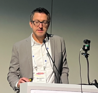
Benjamin Lee, a senior research scientist at Nvidia, in his ECOC address, discussed the high-performance computing market and the role graphics processing units (GPUs) play in accelerating artificial intelligence and machine learning tasks.
Nvidia not only develops processors, GPUs and data processing unit ICs but also networking silicon and systems that the company uses to make high-performance computing systems.
Lee’s talk addressed the role optical interconnect will play in ensuring continuing scaling of high-performance GPU-based computing systems.
Scaled systems
Nvidia’s latest GPU, announced earlier this year, is the 80-billion-transistor Hopper H100. The H100 deliver a six-fold improvement in throughput compared to Nvidia’s existing A100 GPU announced in 2020.
The Hopper is Nvidia’s first GPU that uses the latest generation of stacked DRAM memory, known as high bandwidth memory 3 (HBM3). In addition, Hopper also uses Nvidia’s fourth-generation NVlink interface.
Eight H100 GPUs fit within Nvidia’s DGX box, as do four Nvidia NVSwitches used to interconnect the GPUs. In addition, an Nvidia Superpod connects 32 DGX nodes – 256 GPUs – using an external tier of NVSwitches.
“A paradigm shift we’re seeing is that switched interconnect is becoming important for scale-up,” said Lee. “So when we want to make the node more computationally powerful, those switches are being put inside the box to connect the GPUs.”
Switch ASIC bandwidths are consistently improving, with 51.2-terabit switch silicon being state-of-the-art. But despite such progress, the scaling is insufficient to keep up with bandwidth requirements, said Lee.
Switch ASIC power consumption is also rising, with advanced CMOS scaling having less impact on designs. Lee foresees switch ASICs consuming 2kW if current trends continue.
In turn, ASIC input-output (I/O) accounts for an increasing portion of the chip’s overall power consumption.
This is true for Nvidia’s GPUs and switch chips, so any I/O technology developed for switching will also benefit its GPUs.
Thus, Nvidia sees optical I/O as the key to scaling the processing performance of its ASICs and computing systems.
I/O metrics
Lee outlined various metrics when discussing optical I/O:
- the electrical interfaces used between the ASIC and optics, and their reach
- the power consumption of the module (the chip, and the chip and optics)
- the system power (of the line card or platform)
- interface density: the capacity exiting a millimetre of surface in terabits-per-second-per-mm (Tbps/mm)
For a system using a 102.4-terabit switch IC, half the power is consumed by the ASIC and half by the edge-board pluggable optics. Here the OIF’s long reach (LR) interface links the two.
The chip’s electrical interfaces consume 4.5 to 6.5 picojoule-per-bit (pJ/b) such that the total switch IC I/O power consumed is 450W.
The next step is co-packaged optics. Here, optical chiplets are placed closer to the ASIC (100mm away) such that the OIF’s lower power XSR (extra short reach) interface can be used that consumes 1.24-1.7pJ/s, says Lee.
Again taking a module view, Nvidia views the co-packaged design as comprising two electrical interfaces (the XSR interface between the chip and optical chiplets either side) and one optical interface.
This equates to 250W per chip module, a modest power saving at the chip module level but a significant power saving at the system level, given the optics is now part of the module.
However, bandwidth density is 475-870Gbps/mm, and for beyond 100-terabit switches, a further fourfold improvement is needed: 2Tbps/mm and, ultimately, 10Tbps/mm.
Just achieving a 2Tb/s/mm interface density will be challenging, says Lee.
For that, 2.5D co-packaged optics will be needed with the ASIC and chiplets sharing a silicon interposer that enables higher wire densities.
2.5D integration is already an established technology in the semiconductor industry; Nvidia has been using the technology for its GPUs since 2016.
The technology enables much closer coupling between the ASIC and optics (some 1mm), resulting in sub 1pJ/bit. Nvidia cites research showing a 0.3pJ/b has already been achieved.
Scaling I/O
Lee outlined all the ways I/O can be scaled.
Baud rate is one approach, but the energy efficiency diminishes as the symbol rate increases, from 50 to 100 to 200 gigabaud.
Modulation is another approach, moving from non-return-to-zero to 4-level pulse amplitude modulation (PAM-4) and even higher PAM schemes. The challenge is that the signal-to-noise ratio diminishes the higher the PAM scheme, requiring additional digital signal processing which, in turn, consumes more power.
Another technique, polarization, can be used to double the data rate. Then there is the spatial domain. Here, tighter pitches can be used, says Lee, moving from 250, 127 and even 80 microns before other approaches are needed. These include multi-core fibre, waveguide fan-outs and even bidirectional optics (what Google uses for its optical circuit switch ports, to save on fibre and port count).
All these spatial approaches require considerable development and operational costs, says Lee.
The most promising way to boost throughput and increase interface density is using wavelength division multiplexing (WDM).
Nvidia has produced several generations of test chips that use wavelength parallelism in the O-band based on micro-ring resonators.
Nvidia’s steer
Micro-ring resonator technology already supports 100Gbps modulation rates. The optical circuit is also compact, energy-efficient and supports wavelength scaling.
Lee also outlined other key technologies that will be needed, each bringing their own challenges. One is the external laser source, another is advanced packaging.
Nvidia believes that for future generations of ASICs, dense WDM mirror-ring modulated links offer the most promising approach to meeting both low power and the massive interface density improvements that will be needed.
This will require low-cost lasers while packaging remains a severe challenge.
2.5D integration is going to be an important step in the evolution of switch interconnect, concluded Lee.

Tencent makes its co-packaged optics move

- Tencent is the first hyperscaler to announce it is deploying a co-packaged optics switch chip
- Tencent will use Broadcom’s Humboldt that combines its 25.6-terabit Tomahawk 4 switch chip with four optical engines, each 3.2 terabit-per-second (Tbps)
Part 2: Broadcom’s co-packaged optics
Tencent will use Broadcom’s Tomahawk 4 switch chip co-packaged with optics for its data centres.
“We are now partnered with the hyperscaler to deploy this in a network,” says Manish Mehta, vice president of marketing and operations optical systems division, Broadcom. “This is a huge step for co-packaged optics overall.”
Broadcom demonstrated a working version of a Humboldt switch at OFC earlier this year.
The Chinese hyperscaler will use Broadcom’s 25.6Tbps Tomahawk 4 Humboldt, a hybrid design where half of the chip’s input-output (I/O) is optical and half is the chip’s serialisers-deserialisers (serdes) that connect to pluggable modules on the switch’s front panel.
Four Broadcom 3.2-terabit silicon photonics-based optical engines are co-packaged alongside the Tomahawk 4 chip to implement 12.8Tbps of optical I/O.
Broadcom demonstrated a working version of a Humboldt switch at OFC earlier this year.
Co-packaged optics
Broadcom started its co-packaged optics development work in 2019.
“One of the reasons for our investment in co-packaged optics was that we did see firsthand the ongoing limits of copper interconnect being approached,” says Mehta.
The transmission reach of copper links continues to shrink as the signalling speed has increased from 25 gigabits-per-second (Gbps) non-return to zero (NRZ) to PAM-4 (4-level pulse amplitude modulation) based signalling at 56Gbps, 112Gbps and, in the coming years, 224Gbps. Power consumption is also rising with each speed hike.
Broadcom says data centres now use 1 million optical interconnects, but that much of the connectivity is still copper-based, linking adjacent racks and equipment within the rack.
“Hyperscalers spend ten times more on interconnects than switching silicon,” says Mehta. Given these trends, there needs to be a continual improvement in the power profile, cost and scaled manufacturing of optical interconnect, he says.
In the short term, what is driving interest in co-packaged optics is overcoming the limitations of copper, says Broadcom.
In early 2021, Broadcom detailed at a JP Morgan event its co-packaged optics roadmap. Outlined was the 25.6-terabit Humboldt to be followed by Bailly, a 51.2-terabit all co-packaged optics design using Broadcom’s Tomahawk 5 switch chip which is now sampling.
Humboldt uses DR4 (4×100-gigabit using 4 fibres) whereas the 51.2-terabit Bailly will add multiplexing-demultiplexing and use the FR4 specification (4×100-gigabit wavelengths per fibre).
Technology and partners
Broadcom’s in-house technology includes lasers (VCSELs and EMLs), mixed-signal expertise (trans-impedance amplifiers and drivers), and silicon photonics, as well as its switch chips.
Broadcom uses a remote laser source for its co-packaged optics design. Placing the laser away from the package (the switch chip and optics) means no cooling is needed.
Broadcom is working with 15 partners to enable its co-packaged optics, highlighting the breadth of expertise required and the design complexity.
There are two prominent use cases for the hybrid I/O Humboldt.
One is for top-of-rack switches, where the electrical interfaces support short-reach copper links connecting the servers in a rack, while the optical links connect the top-of-rack box to the next layer of aggregation switching.
The second use is at the aggregation layer, where the electrical I/O connects other switches in the rack while the optical links connect to switch layers above or below the aggregation layer.
“There is a use case for having pluggable ports where you can deploy low-cost direct-attached copper,” says Mehta.
Broadcom says each data centre operator will have their own experience with their manufacturing partners as they deploy co-packaged optics. Tencent has decided to enter the fray with 25.6-terabit switches.
“It is not just Broadcom developing the optical solution; it is also ensuring that our manufacturing partner is ready to scale,” says Mehta.
Ruijie Networks is making the two-rack-unit (2RU) switch platform for Tencent based on Broadcom’s co-packaged optics solution. The co-packaged optics interfaces are routed to 16 MPO connectors while the switch supports 32, 400-gigabit QSFP112 modules.
“It’s always important to have your lead partner [Tencent] for any deployment like this, someone you’re working closely with to get it to market,” says Mehta. “But there is interest from other customers as well.”
Cost and power benefits
Broadcom says co-packaged optics will lower the optical cost-per-bit by 40 per cent while the system (switch platform) power savings will be 30 per cent.
Humboldt more than halves the power compared to using pluggables. Broadcom’s co-packaged optics consumes 7W for each 800-gigabits of bandwidth, whereas an equivalent 800-gigabit optical module consumes 16-18W.
Its second-generation design will embrace 5nm CMOS rather than 7nm and still more than halve the power: an 800-gigabit pluggable will consume 14-15W, whereas it will be 5.5W for the same co-packaged optics bandwidth.
Broadcom will move to CMOS for its second-generation electrical IC; it uses silicon germanium at present.
Power and operational cost savings are a longer-term benefit for data centre operators, says Broadcom. A more immediate concern is the growing challenge of managing the thermal profile when designing switching systems. “The amount of localised heat generation of these components is making systems quite challenging,” says Mehta.
A co-packaged design eliminates pluggables, making system design easier by improving airflow via the front panel and reducing the power required for optical interconnect.
“They’ve been telling us this directly,” says Mehta. “It’s been a pretty good testimonial to the benefits they can see for system design and co-packaged optics.”
Roadmap
At OFC 2022, Broadcom also showed a mock-up of Bailly, a 51.2 terabit switch chip co-packaged with eight 6.4Tbps optical engines.
Broadcom will offer customers a fully co-packaged optics Tomahawk 5 design but has not given a date.
Since Broadcom has consistently delivered a doubling of switch silicon capacity every 24 months, a 102.4-terabit Tomahawk 6 is scheduled to sample in the second half of 2024.
That timescale suggests it will be too early to use 224Gbps serdes being specified by the OIF. Indeed, Mehta believes 112Gbps serdes will have “a very long life”.
That would require the next-generation 102.2Tbps to integrate 1024, 100Gbps serdes on a die. Or, if that proves too technically challenging, then, for the first time, Broadcom’s switching ASIC may no longer be a monolithic die.
Broadcom’s networking group is focused on high-speed serial electrical interfaces. But the company is encouraged by developments such as the open standard UCIe for package interconnect, which looks at slower, wider parallel electrical interfaces to support chiplets. UCIe promises to benefit co-packaged optics.
Broadcom’s view is that it is still early with many of these design challenges.
“Our goal is to understand when we need to be ready and when we need to be launching our silicon on the optical side,” says Mehta. “That’s something we are working towards; it’s still not clear yet.”

II-VI’s VCSEL approach for co-packaged optics
Co-packaged optics was a central theme at this year’s OFC show, held in San Diego. But the solutions detailed were primarily using single-mode lasers and fibre.
The firm II-VI is beating a co-packaged optics path using vertical-cavity surface-emitting lasers (VCSELs) and multi-mode fibre while also pursuing single-mode, silicon photonics-based co-packaged optics.
For multi-mode, VCSEL-based co-packaging, II-VI is working with IBM, a collaboration that started as part of a U.S. Advanced Research Projects Agency-Energy (ARPA-E) project to promote energy-saving technologies.
II-VI claims there are significant system benefits using VCSEL-based co-packaged optics. The benefits include lower power, cost and latency when compared with pluggable optics.
The two key design decisions that achieved power savings are the elimination of the retimer chip – also known as a direct-drive or linear interface – and the use of VCSELs.
The approach – what II-VI calls shortwave co-packaged optics – integrates the VCSELs, chip and optics in the same package.
The design is being promoted as first augmenting pluggables and then, as co-packaged optics become established, becoming the predominant solution for system interconnect.
For every 10,000 QSFP-DD pluggable optical modules used by a supercomputer that are replaced with VCSEL-based co-packaged optics, the yearly electricity bill will be reduced by up to half a million dollars, estimate II-VI and IBM.
VCSEL technology
VCSELs are used for active optical cables and short-reach pluggables for up to 70m or 100m links.
VCSEL-based modules consume fewer watts and are cheaper than single-mode pluggables.
Several factors account for the lower cost, says Vipul Bhatt, vice president of marketing, datacom vertical at II-VI.
The VCSEL emits light vertically from its surface, simplifying the laser-fibre alignment, and multi-mode fibre already has a larger-sized core compared to single-mode fibre.
“Having that perpendicular emission from the laser chip makes manufacturing easier,” says Bhatt. “And the device’s small size allows you to get many more per wafer than you can with edge-emitter lasers, benefitting cost.”
The tinier VCSEL also requires a smaller current density to work; the threshold current of a distributed feedback (DFB) laser used with single-mode fibre is 25-30mA, whereas it is 5-6mA for a VCSEL. “That saves power,” says Bhatt.
Fibre plant
Hyperscalers such as Google favour single-mode fibre for their data centres. Single-mode fibre supports longer reach transmissions, while Google sees its use as future-proofing its data centres for higher-speed transmissions.
Chinese firms Alibaba and Tencent use multi-mode fibre but also view single-mode fibre as desirable longer term.
Bhatt says he has been hearing arguments favouring single-mode fibre for years, yet VCSELs continue to advance in speed, from 25 to 50 to 100 gigabits per lane.
“VCSELs continue to lead in cost and power,” says Bhatt. ”And the 100-gigabit-per-lane optical link has a long life ahead of it, not just for networking but machine learning and high-performance computing.“
II-VI says single-mode fibre and silicon photonics modules are suited for the historical IEEE and ITU markets of enterprise and transport where customers have longer-reach applications.
VCSELs are best suited for shorter reaches such as replacing copper interconnects in the data centre.
Copper interconnect reaches are shrinking as interface speeds increase, while a cost-effective optical solution is needed to support short and intermediate spans up to 70 meters.
“As we look to displace copper, we’re looking at 20 meters, 10 meters, or potentially down to three-meter links using active optical cables instead of copper,” says Bhatt. “This is where the power consumption and cost of VCSELs can be an acceptable premium to copper interconnects today, whereas a jump to silicon photonics may be cost-prohibitive.”
Silicon photonics-based optical modules have higher internal optical losses but they deliver reaches of 2km and 10km.
“If all you’re doing is less than 100 meters, think of the incredible efficiency with which these few milliamps of current pumped into a VCSEL and the resulting light launched directly and efficiently into the fibre,” says Bhatt. “That’s an impressive cost and power saving.”
Applications
The bulk of VCSEL sales for the data centre are active optical cables and short-reach optical transceivers.
“Remember, not every data centre is a hyperscale data centre,” says Bhatt. ”So it isn’t true that multi-mode is only for the server to top-of-rack switch links. Hyperscale data centres also have small clusters for artificial intelligence and machine learning.”
The 100m-reach of VCSELs-based optics means it can span all three switching tiers for many data centres.
The currently envisioned 400-gigabit VCSEL modules are 400GBASE-SR8 and the 8-by-50Gbps 400G-SR4.2. Both use 50-gigabit VCSELs: 25 gigabaud devices with 4-level pulse amplitude modulation (PAM-4).
The 400GBASE-SR8 module requires 16 fibres, while the 400G-SR4.2, with its two-wavelength bidirectional design, has eight fibres.
The advent of 100-gigabit VCSELs (50 gigabaud with PAM-4) enables 800G-SR8, 400G-SR4 and 100G-SR1 interfaces. II-VI first demonstrated a 100-gigabit VCSEL at ECOC 2019, while 100-gigabit VCSEL-based modules are becoming commercially available this year.
Terabit VCSEL MSA
The Terabit Bidirectional (BiDi) Multi-Source Agreement (MSA) created earlier this year is tasked with developing optical interfaces using 100-gigabit VCSELs.
The industry consortium will define 800 gigabits interface over parallel multi-mode fibre, the same four pairs of multi-mode fibre that support the 400-gigabit, 400G-BD4.2 interface. It will also define a 1.6 terabit optical interface.
The MSA work will extend the parallel fibre infrastructure from legacy 40 gigabits to 1.6 terabits as data centres embrace 25.6-terabit and soon 51.2-terabit switches.
Founding Terabit BiDi MSA members include II-VI, Alibaba, Arista Networks, Broadcom, Cisco, CommScope, Dell Technologies, HGGenuine, Lumentum, MACOM and Marvell Technology.
200-gigabit lasers and parallelism
The first 200-gigabit electro-absorption modulator lasers (EMLs) were demonstrated at OFC ’22, while the next-generation 200-gigabits directly modulated lasers (DMLs) are still in the lab.
When will 200-gigabit VCSELs arrive?
Bhatt says that while 200-gigabit VCSELs were considered to be research-stage products, recent interest in the industry has spurred the VCSEL makers to accelerate the development timeline.
Bhatt repeats that VCSELs are best suited for optimised short-reach links.
“You have the luxury of making tradeoffs that longer-reach designs don’t have,” he says. “For example, you can go parallel: instead of N-by-200-gig lanes, it may be possible to use twice as many 100-gig lanes.”
VCSEL parallelism for short-reach interconnects is just what II-VI and IBM are doing with shortwave co-packaged optics.
Shortwave co-packaged optics
Computer architectures are undergoing significant change with the emergence of accelerator ICs for CPU offloading.
II-VI cites such developments as Nvidia’s Bluefield data processing units (DPUs) and the OpenCAPI Consortium, which is developing interface technology so that any microprocessor can talk to accelerator and I/O devices.
“We’re looking at how to provide a high-speed, low-latency fabric between compute resources for a cohesive fabric,” says Bhatt. The computational resources include processors and accelerators such as graphic processing units (GPUs) and field-programmable gate arrays (FPGAs).
II-VI claims that by using multi-mode optics, one can produce the lowest power consumption optical link feasible, tailored for very-short electrical link budgets.
The issue with pluggable modules is connecting them to the chip’s high-speed signals across the host printed circuit board (PCB).
“We’re paying a premium to have that electrical signal reach through,” says Bhatt. “And where most of the power consumption and cost are is those expensive chips that compensate these high-speed signals over those trace lengths on the PCB.”
Using shortwave co-packaged optics, the ASIC can be surrounded by VCSEL-based interfaces, reducing the electrical link budget from some 30cm for pluggables to links only 2-3cm long.
“We can eliminate those very expensive 5nm or 7nm ICs, saving money and power,” says Bhatt.
The advantage of shortwave co-packaged optics is better performance (a lower error rate) and lower latency (between 70-100ns) which is significant when connecting to pools of accelerators or memory.
“We can reduce the power from 15W for a QSFP-DD module down to 5W for a link of twice the capacity,” says Bhatt, “We are talking an 80 per cent reduction in power dissipation. Another important point is that when power capacity is finite, every watt saved in interconnects is a watt available to add more servers. And servers bring revenue.”
This is where the 10,000-unit optical interfaces, $0.4-$0.5 million savings in yearly electricity costs comes from.
The power savings arise from the VCSEL’s low drive current, the use of the OIF’s ultra short-reach (USR) electrical interface and the IBM processor driving the VCSEL directly, what is called a linear analogue electrical interface.
In the first co-packaged optics implementation, IBM and II-VI use non-return-to-zero (NRZ) signalling.
The shortwave co-packaged optics has a reach of 20m which enables the potential elimination of top-of-rack switches, further saving costs. (See diagram.)

II-VI sees co-packaged optics as initially augmenting pluggables. With next-generation architectures using 1.6-terabit OSFP-XD pluggables, 20 to 40 per cent of those ports are for sub-20m links.
“We could have 20 to 40 per cent of the switch box populated with shortwave co-packaged optics to provide those links,” says Bhatt.
The remaining ports could be direct-attached copper, longer-reach silicon-photonics modules, or VCSEL modules, providing the flexibility associated with pluggables.
“We think shortwave co-packaged optics augments pluggables by helping to reduce power and cost of next-generation architectures.”
This is the secret sauce of every hyperscaler. They don’t talk about what they’re doing regarding machine learning and their high-performance systems, but that’s where they strive to differentiate their architectures, he says.
Status
Work has now started on a second-generation shortwave design that will use PAM-4 signalling. “That is targeted as a proof-of-concept in the 2024 timeframe,” says Bhatt.
The second generation will enable a direct comparison in terms of power, speed and bandwidth with single-mode co-packaged optics designs.
Meanwhile, II-VI is marketing its first-phase NRZ-based design.
“Since it is an analogue front end, it’s truly rate agnostic,” says Bhatt. “So we’re pitching it as a low-latency, low-power bandwidth density solution for traditional 100-gigabit Ethernet.”
The design also can be used for next-generation PCI Express and CXL disaggregated designs.
II-VI says there is potential to recycle hyperscaler data centre equipment by adding state-of-the-art network fabric to enable pools of legacy processors. “This technology delivers that,” says Bhatt.
But II-VI says the main focus is for accelerator fabrics: proprietary interfaces like NVlink, Fujitsu’s Tofu interconnect or HPE’s Cray’s Slingshot.
“At some point, memory pools or storage pools will also work their way into the hyperscalers’ data centres,” says Bhatt.

The various paths to co-packaged optics

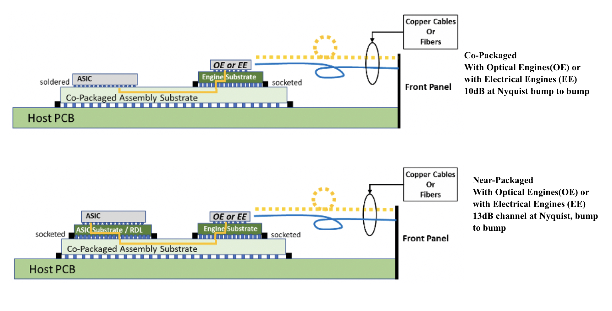
Near package optics has emerged as companies have encountered the complexities of co-packaged optics. It should not be viewed as an alternative to co-packaged optics but rather a pragmatic approach for its implementation.
Co-packaged optics will be one of several hot topics at the upcoming OFC show in March.
Placing optics next to silicon is seen as the only way to meet the future input-output (I/O) requirements of ICs such as Ethernet switches and high-end processors.
For now, pluggable optics do the job of routing traffic between Ethernet switch chips in the data centre. The pluggable modules sit on the switch platform’s front panel at the edge of the printed circuit board (PCB) hosting the switch chip.
But with switch silicon capacity doubling every two years, engineers are being challenged to get data into and out of the chip while ensuring power consumption does not rise.
One way to boost I/O and reduce power is to use on-board optics, bringing the optics onto the PCB nearer the switch chip to shorten the electrical traces linking the two.
The Consortium of On-Board Optics (COBO), set up in 2015, has developed specifications to ensure interoperability between on-board optics products from different vendors.
However, the industry has favoured a shorter still link distance, coupling the optics and ASIC in one package. Such co-packaging is tricky which explains why yet another approach has emerged: near package optics.
I/O bottleneck
“Everyone is looking for tighter and tighter integration between a switch ASIC, or ‘XPU’ chip, and the optics,” says Brad Booth, president at COBO and principal engineer, Azure hardware architecture at Microsoft. XPU is the generic term for an IC such as a CPU, a graphics processing unit (GPU) or even a data processing unit (DPU).
What kick-started interest in co-packaged optics was the desire to reduce power consumption and cost, says Booth. These remain important considerations but the biggest concern is getting sufficient bandwidth on and off these chips.
“The volume of high-speed signalling is constrained by the beachfront available to us,” he says.
Booth cites the example of a 16-lane PCI Express bus that requires 64 electrical traces for data alone, not including the power and ground signalling. “I can do that with two fibres,” says Booth.

Near package optics
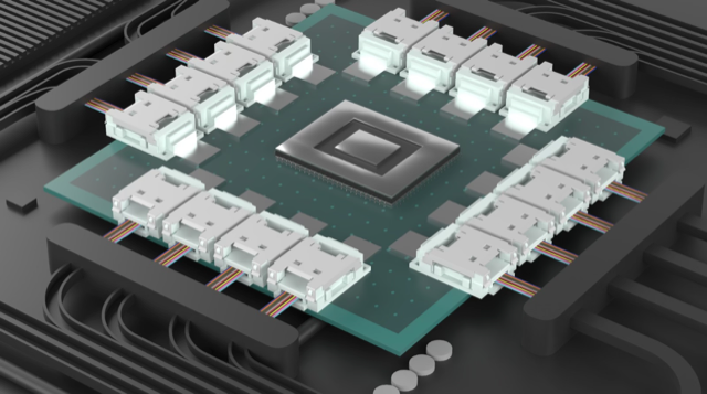
With co-packaged optics, the switch chip is typically surrounded by 16 optical modules, all placed on an organic substrate (see diagram below).
“Another name for it is a multi-chip module,” says Nhat Nguyen, senior director, solutions architecture at optical I/O specialist, Ayar Labs.
A 25.6-terabit Ethernet switch chip requires 16, 1.6 terabits-per-second (1.6Tbps) optical modules while upcoming 51.2-terabit switch chips will use 3.2Tbps modules.
“The issue is that the multi-chip module can only be so large,” says Nguyen. “It is challenging with today’s technology to surround the 51.2-terabit ASIC with 16 optical modules.”
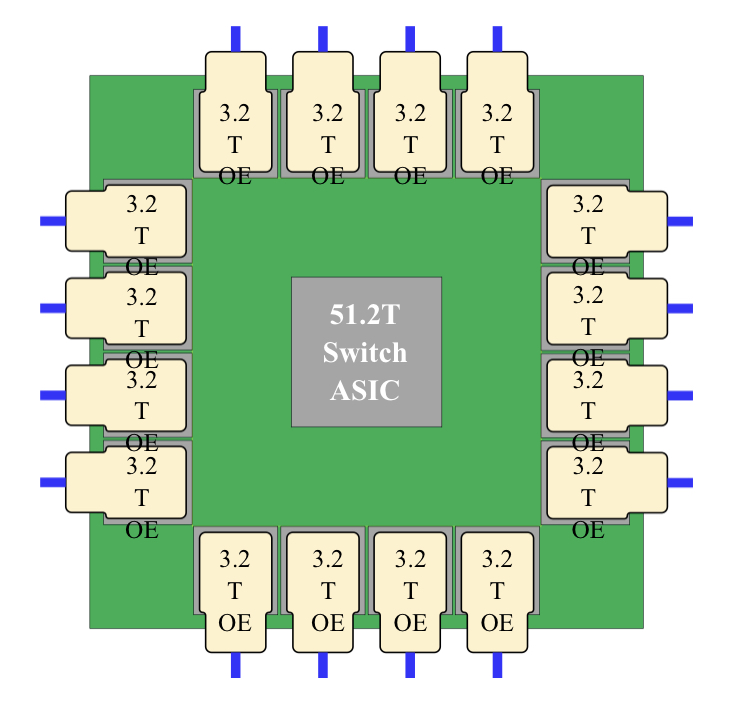
Near package optics tackles this by using a high-performance PCB substrate – an interposer – that sits on the host board, in contrast to co-packaged optics where the modules surround the chip on a multi-chip module substrate.
The near package optics’ interposer is more spacious, making the signal routing between the chip and optical modules easier while still meeting signal integrity requirements. Using the interposer means the whole PCB doesn’t need upgrading which would be extremely costly.
Some co-packaged optics design will use components from multiple suppliers. One concern is how to service a failed optical engine when testing the design before deployment. “That is one reason why a connector-based solution is being proposed,” says Booth. “And that also impacts the size of the substrate.”

A larger substrate is also needed to support both electrical and optical interfaces from the switch chip.
Platforms will not become all-optical immediately and direct-attached copper cabling will continue to be used in the data centre. However, the issue with electrical signalling, as mentioned, is it needs more space than fibre.
“We are in a transitional phase: we are not 100 per cent optics, we are not 100 per cent electrical anymore,” says Booth. “How do you make that transition and still build these systems?”
Perspectives
Ayar Labs views near package optics as akin to COBO. “It’s an attempt to bring COBO much closer to the ASIC,” says Hugo Saleh, senior vice president of commercial operations and managing director of Ayar Labs U.K.
However, COBO’s president, Booth, stresses that near package optics is different from COBO’s on-board optics work.
“The big difference is that COBO uses a PCB motherboard to do the connection whereas near package optics uses a substrate,” he says. “It is closer than where COBO can go.”
It means that with near package optics, there is no high-speed data bandwidth going through the PCB.
Booth says near package optics came about once it became obvious that the latest 51.2-terabit designs – the silicon, optics and the interfaces between them – cannot fit on even the largest organic substrates.
“It was beyond the current manufacturing capabilities,” says Booth. “That was the feedback that came back to Microsoft and Facebook (Meta) as part of our Joint Development Foundation.”
Near package optics is thus a pragmatic solution to an engineering challenge, says Booth. The larger substrate remains a form of co-packaging but it has been given a distinct name to highlight that it is different to the early-version approach.
Nathan Tracy, TE Connectivity and the OIF’s vice president of marketing, admits he is frustrated that the industry is using two terms since co-packaged optics and near package optics achieve the same thing. “It’s just a slight difference in implementation,” says Tracy.
The OIF is an industry forum studying the applications and technology issues of co-packaging and this month published its framework Implementation Agreement (IA) document.
COBO is another organisation working on specifications for co-packaged optics, focussing on connectivity issues.
Technical differences
Ayar Labs highlights the power penalty using near package optics due to its use of longer channel lengths.
For near package optics, lengths between the ASIC and optics can be up to 150mm with the channel loss constrained to 13dB. This is why the OIF is developing the XSR+ electrical interface, to expand the XSR’s reach for near package optics.
In contrast, co-packaged optics confines the modules and host ASIC to 50mm of each other. “The channel loss here is limited to 10dB,” says Nguyen. Co-packaged optics has a lower power consumption because of the shorter spans and 3dB saving.
Ayar Labs highlights its optical engine technology, the TeraPHY chiplet that combines silicon photonics and electronics in one die. The optical module surrounding the ASIC in a co-packaged design typically comprises three chips: the DSP, electrical interface and photonics.
“We can place the chiplet very close to the ASIC,” says Nguyen. The distance between the ASIC and the chiplet can be as close as 3-5mm. Whether on the same interposer Ayar Labs refers to such a design using athird term: in-package optics.
Ayar Labs says its chiplet can also be used for optical modules as part of a co-packaged design.
The very short distances using the chiplet result in a power efficiency of 5pJ/bit whereas that of an optical module is 15pJ/bit. Using TeraPHY for an optical module co-packaged design, the power efficiency is some 7.5pJ/bit, half that of a 3-chip module.
A 3-5mm distance also reduces the latency while the bandwidth density of the chiplet, measured in Gigabit/s/mm, is higher than the optical module.
Co-existence
Booth refers to near package optics as ‘CPO Gen-1’, the first generation of co-packaged optics.
“In essence, you have got to use technologies you have in hand to be able to build something,” says Booth. “Especially in the timeline that we want to demonstrate the technology.”
Is Microsoft backing near package optics?

“We are definitely saying yes if this is what it takes to get the first level of specifications developed,” says Booth.
But that does not mean the first products will be exclusively near package optics.
“Both will be available and around the same time,” says Booth. “There will be near packaged optics solutions that will be multi-vendor and there will be more vertically-integrated designs; like Broadcom, Intel and others can do.”
From an end-user perspective, a multi-vendor capability is desirable, says Booth.
Ayar Labs’ Saleh sees two developing paths.
The first is optical I/O to connect chips in a mesh or as part of memory semantic designs used for high-performance computing and machine learning. Here, the highest bandwidth and lowest power are key design goals.
Ayar Labs has just announced a strategic partnership with high performance computing leader, HPE, to design future silicon photonics solutions for HPE’s Slingshot interconnect that is used for upcoming Exascale supercomputers and also in the data centre.
The second path concerns Ethernet switch chips and here Saleh expects both solutions to co-exist: near package optics will be an interim solution with co-packaged optics dominating longer term. “This will move more slowly as there needs to be interoperability and a wide set of suppliers,” says Saleh.
Booth expects continual design improvements to co-packaged optics. Further out, 2.5D and 3D chip packaging techniques, where silicon is stacked vertically, to be used as part of co-packaged optics designs, he says.

Intel sets a course for scalable optical input-output

- Intel is working with several universities to create building-block circuits to address its optical input-output (I/O) needs for the next decade-plus.
- By 2024 the company wants to demonstrate the technologies achieving 4 terabits-per-second (Tbps) over a fibre at 0.25 picojoules-per-bit (pJ/b).
Intel has teamed up with seven universities to address the optical I/0 needs for several generations of upcoming products.
The initiative, dubbed the Intel Research Center for Integrated Photonics for Data Centre Interconnects, began six months ago and is a three-year project.
No new location is involved, rather the research centre is virtual with Intel funding the research. By setting up the centre, Intel’s goal is to foster collaboration between the research groups.
Motivation
James Jaussi, senior principal engineer and director of the PHY Research Lab in Intel Labs, (pictured) heads a research team that focuses on chip-to-chip communication involving electrical and optical interfaces.
“My team is primarily focussed on optical communications, taking that technology and bringing it close to high-value silicon,” says Jaussi.
Much of Jaussi’s 20 years at Intel has focussed on electrical I/O. During that time, the end of electrical interfaces has repeatedly been predicted. But copper’s demise has proved overly pessimistic, he says, given the advances made in packaging and printed circuit board (PCB) materials.
But now the limits of copper’s bandwidth and reach are evident and Intel’s research arm wants to ensure that when the transition to optical occurs, the technology has longevity.
“This initiative intends to prolong the [optical I/O] technology so that it has multiple generations of scalability,” says Jaussi. And by a generation, Jaussi means the 3-4 years it takes typically to double the bandwidth of an I/O specification.
Co-packaged optics and optical I/O
Jaussi distinguishes between co-packaged optics and optical I/O.
He describes co-packaged optics as surrounding a switch chip with optics. Given the importance of switch chips in the data centre, it is key to maintain compatibility with specifications, primarily Ethernet.
But that impacts the power consumption of co-packaged optics. “The power envelope you are going to target for co-packaged optics is not necessarily going to meet the needs of what we refer to as optical I/O,” says Jaussi.
Optical I/O involves bringing the optics closer to ICs such as CPUs and graphics processor units (GPUs). Here, the optical I/O need not be aligned with standards.
The aim is to take the core I/O off a CPU or GPU and replace it with optical I/O, says Jaussi.
With optical I/O, non-return-to-zero (NRZ) signalling can be used rather than 4-level pulse amplitude modulation (PAM-4). The data rates are slower using NRZ but multiple optical wavelengths can be used in parallel. “You can power-optimise more efficiently,” says Jaussi.
Ultimately, co-packaged optics and optical I/O will become “stitched together” in some way, he says.
Research directions
One of the research projects involves the work of Professor John Bowers and his team at the University of California, Santa Barbara, on the heterogeneous integration of next-generation lasers based on quantum-dot technology.
Intel’s silicon photonics transceiver products use hybrid silicon quantum well lasers from an earlier collaboration with Professor Bowers.
The research centre work is to enable scalability by using multi-wavelength designs as well as enhancing the laser’s temperature performance to above 100oC. This greater resilience to temperature helps the laser’s integration alongside high-performance silicon.
Another project, that of Professor Arka Majumdar at the University of Washington, is to develop non-volatile reconfigurable optical switching using silicon photonics.
“We view this as a core building block, a capability,” says Jaussi. The switching element will have a low optical loss and will require liitle energy for its control.
The switch being developed is not meant to be a system but an elemental building block, analogous to a transistor, Intel says, with the research exploring the materials needed to make such a device.
The work of Professor S.J. Ben Yoo at University of California, Davis, is another of the projects.
His team is developing a silicon photonics-based modulator and a photodetector technology to enable 40-terabit transceivers at 150fJ/bit and achieving 16Tb/s/mm I/O density.
“The intent is to show over a few fibres a massive amount of bandwidth,” says Jaussi.
Goals
Intel says each research group has its own research targets that will be tracked.
All the device developments will be needed to enable the building of something far more sophisticated in future, says Jaussi.
At Intel Labs’ day last year, the company spoke about achieving 1Tbps of I/O at 1pJ/s. The research centre’s goals are more ambitious: 4Tbps over a fibre at 0.25pJ/b in the coming three years.
There will be prototype demonstrations showing data transmissions over a fibre or even several fibres. “This will allow us to make that scalable not just for one but two, four, 10, 20, 100 fibres,” he says. “That is where that parallel scalability will come from.”
Intel says it will be years before this technology is used for products but the research goals are aggressive and will set the company’s optical I/O goals.
Preparing for a post-pluggable optical module world

Part 1: OIF: ELSFP, XSR+, and CEI-112G-Linear
The OIF is working on several electrical and optical specifications as the industry looks beyond pluggable optical transceivers.
One initiative is to specify the external laser source used for co-packaged optics, dubbed the External Laser Small Form Factor Pluggable (ELSFP) project.
Industry interest in co-packaged optics, combining an ASIC and optical chiplets in one package, is growing as it becomes increasingly challenging and costly to route high-speed electrical signals between a high-capacity Ethernet switch chip and the pluggable optics on the platform’s faceplate.
The OIF is also developing 112-gigabit electrical interfaces to address not just co-packaged optics but also near package optics and the interface needs of servers and graphics processor units (GPUs).
Near package optics also surrounds the ASIC with optical chiplets. But unlike co-packaged optics, the ASIC and chiplets are placed on a high-performance substrate located on the host board.
ELSFP
Data centre operators have vast experience using pluggables and controlling their operating environment so that they don’t overheat. The thermal management of optics co-packaged with an ASIC that can dissipate hundreds of watts is far trickier.
“Of all the components, the one that hates heat the most is the laser,” says Nathan Tracy, TE Connectivity and the OIF’s vice president of marketing.
Players such as Intel and Juniper have integrated laser technology, allowing them to place the full transceiver on a chip. However, the industry trend is to use an external light source so that the laser is decoupled from the remaining optical transceiver circuitry.
“We bring fibre into and out of the co-packaged optical transceiver so why not add a couple more fibres and bring the laser source into the transceiver as well?” says Tracy.
Two approaches are possible. One is to box the lasers and place them within the platform in a thermally-controlled environment. Alternatively, the lasers can be boxed and placed on the equipment’s faceplate, as pluggable optics are today.
“We know how to do that,” says Tracy. “But it is not a transceiver, it is a module full of lasers.”
Such a pluggable laser approach also addresses a concern of the data centre operators: how to service the optics of a co-packaged design.
The OIF’s ELSFP project is working to specify such a laser pluggable module: its mechanical form factor, electrical interface, how light will exit the module, and its thermal management.
The goal is to develop a laser pluggable that powers up when inserted and has a blind-mate optical interface, ensuring light reaches the co-packaged optics transceivers on the host board with minimal optical loss.
“Optical interfaces are fussy things,” says Tracy. Such interfaces must be well-aligned, clean, and hold tight tolerances, says Tracy: “That is all captured under the term blind-mate.”
Optical fibre will deliver light from the laser module to the co-packaged optics but multi-core fibre may be considered in future.
One issue the OIF is discussing is the acceptable laser output power. The higher the output power, the more the source can be split to feed more co-packaged optics transceivers. But higher-power lasers have eye-safety issues.
Another topic being addressed is the fibre density the form factor should enable. The OIF wants a roadmap to ensure that future co-packaged optics’ needs are also met.
“The industry can then take that specification and go compete in the market, adding their differentiation on top of the standardisation,” says Tracy.
The OIF’s ELSFP members have submitted technical contributions and a draft specification exists. “Now we are in the iterative process with members building on that draft,” says Tracy.
Co-packaged optics and near package optics
As the capacity of switch chips continues to double, more interfaces are needed to get data in and out and the harder it is becoming to route the channels between the chip and the optical modules.
The chip package size is also increasing with the growing aggregate bandwidth and channels, says Tracy. These channels come out via the package’s solder balls that connect to the host board.
“You don’t want to make that ASIC package any bigger than it needs to be; packages have bad parasitics,” says Tracy
For a fully co-packaged design, a switch ASIC is surrounded by 16 optical engines. For next-generation 51.2-terabit switch ASICs, 3.2 terabits-per-second (Tbps) optical engines will be required. Add the optical engines and the switch package becomes even bigger.
“You are starting to get to the point where you are making the package bigger in ways that are challenging the industry,” says Tracy.
Near package optics offers an alternative approach to avoid cramming the optics with the ASIC. Here, the ASIC and the chiplets are mounted on a high-performance substrate that sits on the host card.
“Now the optical engines are a little bit further away from the switching silicon than in the co-packaged optics’ case,” says Tracy.
CEI-112G-Extra Short Reach Plus (XSR+) electrical interface
According to optical I/O specialist, Ayar Labs, near package optics and co-packaged optics have similar optical performance given the optical engines are the same. Where they differ is the electrical interface requirements.
With co-packaged optics, the channel length between the ASIC and the optical engine is up to 50mm and the channel loss is 10dB. With near package optics, the channel length is up to 150mm and a 13dB channel loss.
The OIF’s 112Gbps XSR+ electrical interface is to meet the longer reach needs of near package optics.
“It enables a little bit more margin or electrical channel reach while being focused on power reduction,” says Tracy. “Co-packaged optics is all about power reduction; that is its value-add.”
CEI-112G-Linear
A third ongoing OIF project – the CEI-112-Linear project – also concerns a 112Gbps chip-to-optical engine interface.
The project’s goal is to specify a linear channel so that the chip’s electrical transmitter (serdes) can send data over the link – made up of an optical transmitter and an optical receiver as well as the electrical receiver at the far end – yet requires equalisation for the transmitter and end receiver only.
“A linear link means we understand the transition of the signal from electrical to optical to electrical,” says Tracy. “If we are operating over a linear range then equalisation is straightforward.” That means simpler processing for the signal’s recovery and an overall lower power consumption.
By standardising such a linear interface, multiple chip vendors will be able to drive the optics of multiple I/O chiplet companies.
“Everything is about power savings, and the way to get there is by optimising the link,” says Tracy.
224-gigabit electrical interfaces
The OIF’s next-generation 224Gbps electrical interface work continues to progress. Member input to date has tackled the challenges, opportunities and the technologies needed to double electrical interface speeds.
“We are surveying the playing field to understand where the really hard parts are,” says Tracy.
A White Paper is expected in the coming year that will capture how the industry views the issues and the possible solutions.
“If you have industry consensus then it is easier to start a project addressing the specific implementation to meet the problem,” says Tracy.
First co-packaged optics switches set for next year
Ranovus says two of its lead customers will deploy co-packaged optics next year.
They will deploy 25.6-terabit Ethernet switch chips but these will be proof-of-concept designs rather than volume deployments.
The deployments will be used to assess the software and gain experience with their maintenance including replacing optics if needed.
“I do think 2024 is going to be the volume year,” says Hamid Arabzadeh, CEO of Ranovus, who expects to announce the customers before the year-end.
Disaggregated server untangles compute, memory and storage elements
Applications
Ranovus is focussed on the emerging integrated optical input-output (I/O) market for Ethernet switches and disaggregated server designs.
A disaggregated server untangles the compute, memory and storage elements found on a server card and pools them separately. This enables a CPU or compute node to access far more memory. It also means each of the server elements can be upgraded independently.
Pooling the memory suits artificial intelligence (AI)/ machine learning applications that process huge data sets. Such applications also require considerable computing.
For machine learning applications, graphic processing unit (GPU) chips are tightly coupled in clusters. But it is a challenge to continually grow the number of GPUs in a cluster and support inter-cluster communications using eletrical interfaces.
Data centre operators want processing performance that scales linearly as more GPUs are adding to a cluster and more clusters are used. This requires longer-reach, high-bandwidth, low-latency links. Limiting the power consumption of such links is also key.
Such system design challenges explain the industry’s interest in adding optical I/O to high-end processors like GPUs. The same applies to Ethernet switch-chips that are doubling in capacity every two years. Moving from electrical to optical interfaces promises longer, energy efficient (measured in pJ/bit), low-latency links.
For Ethernet switch designs, the optical I/O end-point bandwidth needed is at least 3.2 terabits per second (Tbps), says Arabzadeh, whereas for AI it is 0.5-1Tbps.
Odin optical engine
Ranovus recently expanded its optical interconnect portfolio by developing an Odin design that doesn’t need an accompanying retimer chip.
The optical engine combines CMOS and silicon photonics circuits in a monolithic chip, resulting in a smaller, cheaper and power-efficient design.
This second-generation Odin means Ranovus can now offer digital and analogue drive options for co-packaged optics and address more cost-conscious applications such as chip interconnect in servers.
Arabzadeh says its first Odin design that uses a retimer chip helped secure its lead customers.
“We have two lead customers where we are doing the co-packaging of their [switch] chips operating at 100-gigabit PAM-4,” he says. “And we also have an AI customer, where their chip talks PCI Express 5.0 (PCIe 5.0) to our Odin.”
Ranovus first unveiled its Odin-8 800-gigabit design at OFC 2020 and demonstrated it sending eight 100 gigabit PAM-4 (4-level pulse-amplitude modulation) signals, each on a separate fibre.
The design includes a digital retimer IC which takes the OIF-standard extra short reach (XSR) signal – for example, from a switch chip – and recreates (retimes) the PAM-4 signal before forwarding it to Ranovus’ chip. Such a configuration is referred to as a digital-drive design.

“This retimer is not a chip we do and it is expensive,” says Arabzadeh. “It also consumes half the power of the [Odin] chiplet design.”
Ranovus also detailed over a year ago its Odin-32 design that supports four wavelengths per fibre for a total bandwidth of 3.2Tbps.
Since then, Ranovus has developed its Odin-8 for use in an 800-gigabit DR8 optical module. The module will sample and be in the hands of customers for testing in the coming quarter.
The Odin-based 800G-DR8 optical module has a power consumption of 13W; 4W less than rival designs, says Arabzadeh, adding that the optical engine is cost-effective at 400 gigabits, even when using half its capacity.
ODIN version 2.0
The latest monolithic chip is an analogue-drive design. It features radio frequency (RF) drivers, trans-impedance amplifiers (TIAs), silicon photonics transmitters and receivers, and control logic to oversee the components.
The chip does away with clock data recovery (CDR) while integrating the TIAs on-chip. This reduces system costs. “We have the first TIA at 100 gigabits in CMOS,” says Arabzadeh.
To work without the retimer, the monolithic chip is placed much closer to the driving ASIC, with both sharing a common substrate. “It works because it is parked right next to the other chip,” says Arabzadeh.
Ranovus uses a software model of a vendor’s ASIC’s serialiser/ deserialiser (serdes) to ensure the serdes will drive its analogue input.
Being an analogue drive, it is bit-rate and protocol agnostic. “This allows us to get customers beyond the Ethernet market,” says Arabzadeh. These include 100-gigabit PAM-4 signals and the PCIe 5.0 protocol, as mentioned.
For machine learning applications, a proprietary protocol can be used between the end points. NVLink, a serial multi-lane communications link developed by Nvidia, is one such protocol.
Arabzadeh says Ranovus has achieved 1 terabit-per-mm in pitch interface densities: “The stuff we have got involved in with folks in machine learning and AI dwarfs the Ethernet market.”
Laser source
Ranovus’ co-packaged designs use an external laser source. But the company has patented technlogy that allows lasers to be attached directly to the monolithic chip.
This is done at the wafer level, before slicing a wafer to its constituent die. As a result, Ranovus now has two Odin-8 optical engines, one that uses an external laser source (Odin-8ELS) and one with integrated lasers (Odin-8IL)
The laser-attach technology suits optical module designs and expands the company’s optical interconnect toolkit.
The industry has yet to decide whether to adopt a digital or analogue drive approach for co-packaged optics, but the latest Odin design means Ranovus can do both.
Packaging
The company has also been addressing the tricky issue of packaging the chip. “The packaging is a very difficult challenge,” says Arabzadeh.
Ranovus has used the Odin-8 to verify its packaging approach. Two sets of eight fibres are required for the optical I/O (a set to send and a set to receive) and four more fibres are used for the external laser source.
The Odin-32 will use the same packaging and fibre count. What will change is the chip that will support four wavelengths per fibre; instead of the single ring resonator modulator per output, four will be used.
Arabzadeh says each ring modulator is 25 micron so using one or four per path has little impact on the chip’s area.
Market development
Ranovus is addressing both the co-packaged optics and module designs with its Odin designs.
At the OFC conference and exhibition this summer, Arista Networks outlined how pluggable optics will be able to address 102.4 terabit Ethernet switches while Microsoft said it expects to deploy co-packaged optics by the second half of 2024.
Because of the uncertainty as to when co-packaged optics will take off, Ranovus will also supply its optics for the 400-gigabit and 800-gigabit pluggable module market.
“That is why we have yet to tape out the Odin-32,” he says. “We didn’t want to have the technology and there is nobody on the other side of it.”
But the key is to have an optical interface portfolio that secures designs early.
“If you can get the wins and through that, modify your chip, then you are designed in,” says Arabzadeh.