
OFC 2025: industry reflections
Gazettabyte is asking industry figures for their thoughts after attending the recent 50th-anniversary OFC show in San Francisco. Here are the first contributions from Huawei’s Maxim Kuschnerov, NLM Photonics’ Brad Booth, LightCounting’s Vladimir Kozlov, and Jürgen Hatheier, Chief Technology Officer, International, at Ciena.
Maxim Kuschnerov, Director of R&D, Huawei
The excitement of last year’s Nvidia’s Blackwell graphics processing unit (GPU) announcement has worn off, and there was a slight hangover at OFC from the market frenzy then.
The 224 gigabit-per-second (Gbps) opto-electronic signalling is reaching mainstream in the data centre. The last remaining question is how far VCSELs will go—30 m or perhaps even further. The clear focus of classical Ethernet data centre optics for scale-out architectures is on the step to 448Gbps-per-lane signalling, and it was great to see many feasibility demonstrations of optical signalling showing that PAM-4 and PAM-6 modulation schemes will be doable.
The show demonstrations either relied on thin-film lithium niobate (TFLN) or the more compact indium-phosphide-based electro-absorption modulated lasers (EMLs), with thin-film lithium niobate having the higher overall optical bandwidth.
Higher bandwidth pure silicon Mach-Zehnder modulators have also been shown to work at a 160-175 gigabaud symbol rate, sufficient to enable PAM-6 but not high enough for PAM-4 modulation, which the industry prefers for the optical domain.
Since silicon photonics has been the workhorse at 224 gigabits per lane for parallel single-mode transceivers, a move away to thin-film lithium niobate would affect the density of the optics and make co-packaged optics more challenging.
With PAM-6 being the preferred modulation option in the electrical channel for 448 gigabit, it begs the question of whether the industry should spend more effort on enabling PAM-6 optical to kill two birds with one stone: enabling native signalling in the optical and electrical domains would open the door to all linear drive architectures, and keep the compact pure-silicon platform in the technology mix for optical modulators. Just as people like to say, “Never bet against copper,” I’ll add, “Silicon photonics isn’t done until Chris Doerr says so.”
If there was one topic hotter than the classical Ethernet evolution, it was the scale-up domain for AI compute architectures. The industry has gone from scale-up in a server to a rack-level scale-up based on a copper backplane. But future growth will eventually require optics.
While the big data centre operators have yet to reach a conclusion about the specifications of density, reach, or power, it is clear that such optics must be disruptive to challenge the classical Ethernet layer, especially in terms of cost.
Silicon photonics appears to be the preferred platform for a potential scale-up, but some vendors are also considering VCSEL arrays. The challenge of merging optics onto the silicon interposer along with the xPU is a disadvantage for VCSELs in terms of tolerance to high-temperature environments.
Reliability is always discussed when discussing integrated optics, and several studies were presented showing that optical chips hardly ever fail. After years of discussing how unreliable lasers seem, it’s time to shift the blame to electronics.
But before the market can reasonably attack optical input-output for scale-up, it has to be seen what the adoption speed of co-packaged optics will be. Until then, linear pluggable optics (LPO) or linear retimed optics (LRO) pluggables will be fair game in scaling up AI ‘pods’ stuffed with GPUs.
Brad Booth, CEO of NLM Photonics
At OFC, the current excitement in the photonics industry was evident due to the growth in AI and quantum technologies. Many of the industry’s companies were represented at the trade show, and attendance was excellent.
Nvidia’s jump on the co-packaged optics bandwagon has tipped the scales in favour of the industry rethinking networking and optics.
What surprised me at OFC was the hype around thin-film lithium niobate. I’m always concerned when I don’t understand why the hype is so large, yet I have still to see the material being adopted in the datacom industry.
Vladimir Kozlov, CEO of LightCounting
This year’s OFC was a turning point for the industry, a mix of excitement and concern for the future. The timing of the tariffs announced during the show made the event even more memorable.
This period might prove to be a peak of the economic boom enabled by several decades of globalisation. It may also be the peak in the power of global companies like Google and Meta and their impact on our industry.
More turbulence should be expected, but new technologies will find their way to the market.
Progress is like a flood. It flows around and over barriers, no matter what they are. The last 25 years of our industry is a great case study.
We are now off for another wild ride, but I look forward to OFC 2050.
Jürgen Hatheier, Chief Technology Officer, International, at Ciena
This was my first trip to OFC, and I was blown away. What an incredible showcase of the industry’s most innovative technology
One takeaway is how AI is creating a transformative effect on our industry, much like the cloud did 10 years ago and smartphones did 20 years ago.
This is an unsurprising observation. However, many outside our industry do not realise the critical importance of optical technology and its role in the underlying communication network. While most of the buzz has been on new AI data centre builds and services, the underlying network has, until recently, been something of an afterthought.
All the advanced demonstrations and technical discussions at OFC emphasise that AI would not be possible without high-performance network infrastructure.
There is a massive opportunity for the optical industry, with innovation accelerating and networking capacity scaling up far beyond the confines of the data centre.
The nature of AI — its need for intensive training, real-time inferencing at the edge, and the constant movement of data across vast distances between data centres — means that networks are evolving at pace. We’re seeing a significant architectural shift toward more agile, scalable, and intelligent infrastructure with networks that can adapt dynamically to AI’s distributed, data-hungry nature.
The diversity of optical innovation presented at the conference ranged from futuristic Quantum technologies to technology on the cusp of mainstream adoption, such as 448-gigabit electrical lanes.
The increased activity and development around high-speed pluggables also show how critical coherent optics has become for the world’s most prominent computing players.

ECOC 2023 industry reflections - Part 2
Gazettabyte is asking industry figures for their thoughts after attending the recent ECOC show in Glasgow. In particular, what developments and trends they noted, what they learned and what, if anything, surprised them. Here are more responses from LightCounting, Hyper Photonix, NewPhotonics, and Broadcom.
Vladimir Kozlov, CEO of LightCounting, a market research company
Demand for optical connectivity in data centres has accelerated innovation in the industry. ECOC 2023 offered numerous start-ups and established vendors another opportunity to disclose their latest achievements.
The improved reliability of quantum dot lasers was a pleasant surprise. Alfalume presented the latest quantum dot comb laser developments, including continuous power up to 250 mW with a power conversion efficiency of a quarter (25%) and efficient operation of up to 100oC. Preliminary test data suggests that quantum dot lasers offer superior reliability compared to their quantum well counterparts. It would be great to have a reliable laser source, finally.
Cisco and Intel deserve much credit for bringing silicon photonics-based transceivers to the market, but numerous vendors are entering the race now.
All the leading foundries offer photonic integrated circuits with integrated laser chips. TSMC disclosed its plans to use a 7nm CMOS process to manufacture photonic chips. Recently formed OpenLight offers fully tested photonic integrated circuit designs, which can be produced at several foundries, including Tower Semiconductor.
Many transceiver suppliers have internally designed optical engines. They all plan to reduce the manufacturing cost of silicon photonics-based transceivers, fulfilling the potential of CMOS technology. Competition among suppliers enabled huge reductions in the cost of CMOS-based ICs. Let us see if this works for CMOS-based photonic integrated circuits.
Brad Booth, director of technology and strategy at Hyper Photonix, and a consultant
There was good attendance at ECOC considering some companies continue to limit travel. Linear drive pluggable optics (LPO) is gaining traction but still has hurdles to address. Meanwhile, the 800-gigabit train is pulling into the station with a ZR digital signal processor and client-side modules.
What surprised me at the show? The shift to start-ups. It is reminiscent of the Gigabit Ethernet days.
Yaniv BenHaim, founder & CEO of NewPhotonics
There were some notable trends at ECOC. One is that 800-gigabit optical transceivers are ramping. At least three vendors were giving private demos of 8×100-gigabit DR enabled with the coming availability of 200G EMLs and photodetectors.
The industry is also optimistic about linear drive pluggable optics (LPO), helped by the buzz created by Nvidia, saying it will make the technology available in AI clusters by year-end. Data centres and networking companies are also pushing LPO and evaluating it and will likely announce findings by OFC 2024.
Another upcoming technology, like optical processing, as demonstrated by our company, NewPhotonics, can further advance power savings and range with both traditional optical modules and LPOs. At ECOC, we showed 224 gigabit-per-second (Gbps) optical input-output driving more than 10km of fibre using Intel’s new 224Gbps serialiser-deserialiser (serdes). We also showed NewPhotonics’ optical serdes multiplexing and demultiplexing multiple optical 112Gbps PAM-4 in the optical time domain.
Companies providing coherent technology continue to promote using coherent transceivers in the data centre. We don’t see any reason to do so when PAM-4 non-coherent solutions can cater for data centre needs and also go beyond 10km.
The market is moving forward in using 224 gigabits, which will disrupt optical transceivers and the active optical cable markets. It seems co-packaged optics will be delayed further as the electrical solutions for 50-terabit and 100-terabit switches are already there using electrical serdes.
The optical communication market had no new surprises based on wavelength division multiplexing PAM-4 and 16-QAM. Some ideas exist for replacing the DSP functions with analogue implementations. NewPhotonics is the only company pushing for an all-optical solution instead of an analogue or a digital signal processor solution.
Rajiv Pancholy, director of hyperscale strategy & products, optical systems division at Broadcom
It was evident at ECOC 2023 that the emergence of large networking clusters enabling the connectivity of graphics processing units (GPUs) for recommendation engines and large language models has substantially increased the ratio of photonic to copper links inside data centres. The optics industry has been waiting for an all-to-all connectivity killer app to increase volumes and therefore investment, and that app might have arrived.
Companies demonstrated excellent progress on 200 gigabit per lane optical components. Several companies are sampling 200 gigabit EMLs and plan production in 2024. Several companies also announced plans to release 200 gigabit per lane VCSELs. There was some early demonstration of 200 gigabit per lane silicon photonics, but it is still being determined when the technology will be ready for production.
Lastly, start-ups at the show focused on delivering novel optical interconnect technologies with micro-LEDs, comb lasers, and advanced packaging that reinforces a general trend towards high-density photonic integrated circuits, electrical interconnect simplification, and co-packaging. Though it’s still being determined when these optical technologies will come to market, Broadcom is not the only company working on co-packaged optics. We believe you will need co-packaged optics much sooner than five years from now.

The various paths to co-packaged optics

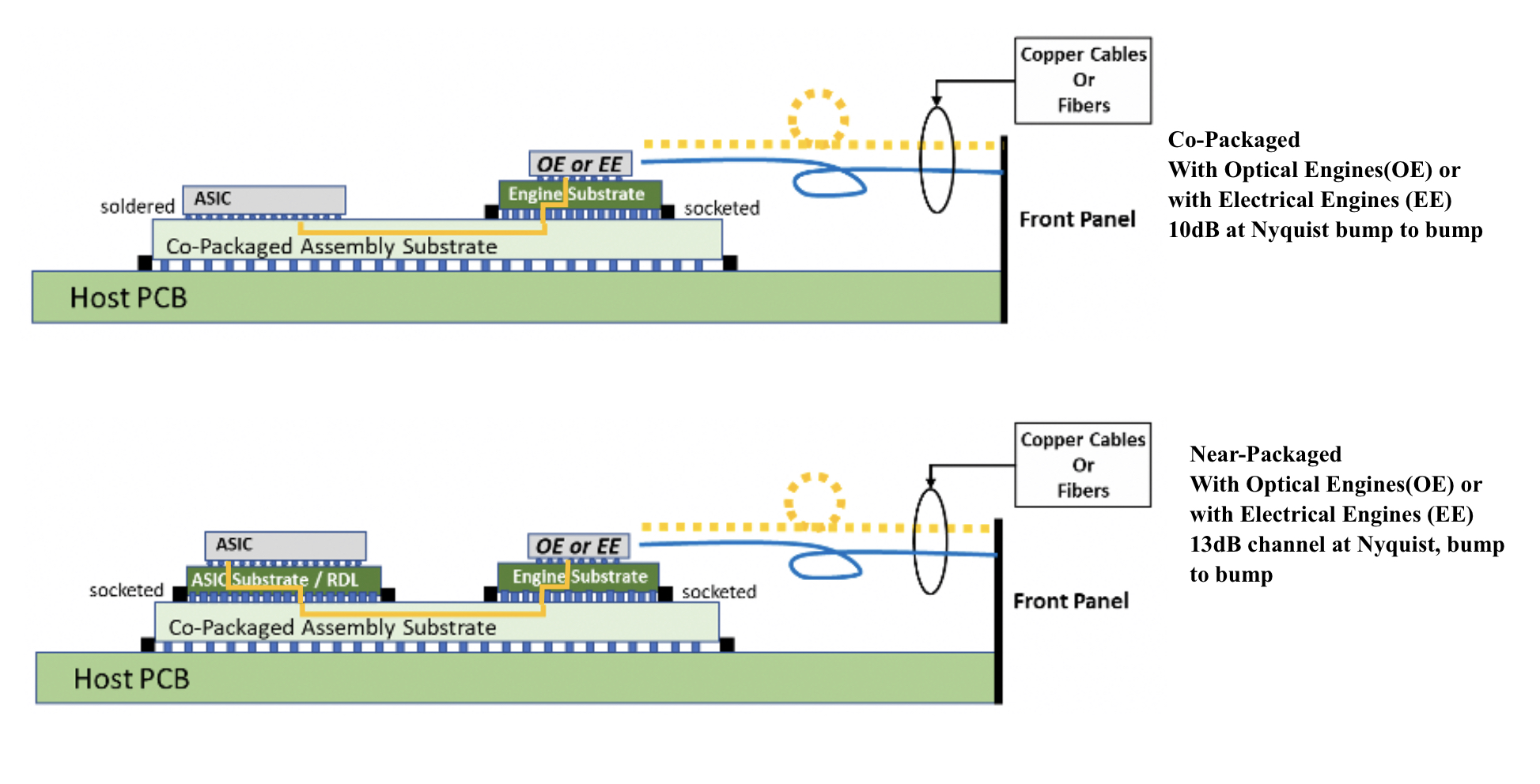
Near package optics has emerged as companies have encountered the complexities of co-packaged optics. It should not be viewed as an alternative to co-packaged optics but rather a pragmatic approach for its implementation.
Co-packaged optics will be one of several hot topics at the upcoming OFC show in March.
Placing optics next to silicon is seen as the only way to meet the future input-output (I/O) requirements of ICs such as Ethernet switches and high-end processors.
For now, pluggable optics do the job of routing traffic between Ethernet switch chips in the data centre. The pluggable modules sit on the switch platform’s front panel at the edge of the printed circuit board (PCB) hosting the switch chip.
But with switch silicon capacity doubling every two years, engineers are being challenged to get data into and out of the chip while ensuring power consumption does not rise.
One way to boost I/O and reduce power is to use on-board optics, bringing the optics onto the PCB nearer the switch chip to shorten the electrical traces linking the two.
The Consortium of On-Board Optics (COBO), set up in 2015, has developed specifications to ensure interoperability between on-board optics products from different vendors.
However, the industry has favoured a shorter still link distance, coupling the optics and ASIC in one package. Such co-packaging is tricky which explains why yet another approach has emerged: near package optics.
I/O bottleneck
“Everyone is looking for tighter and tighter integration between a switch ASIC, or ‘XPU’ chip, and the optics,” says Brad Booth, president at COBO and principal engineer, Azure hardware architecture at Microsoft. XPU is the generic term for an IC such as a CPU, a graphics processing unit (GPU) or even a data processing unit (DPU).
What kick-started interest in co-packaged optics was the desire to reduce power consumption and cost, says Booth. These remain important considerations but the biggest concern is getting sufficient bandwidth on and off these chips.
“The volume of high-speed signalling is constrained by the beachfront available to us,” he says.
Booth cites the example of a 16-lane PCI Express bus that requires 64 electrical traces for data alone, not including the power and ground signalling. “I can do that with two fibres,” says Booth.

Near package optics
With co-packaged optics, the switch chip is typically surrounded by 16 optical modules, all placed on an organic substrate (see diagram below).
“Another name for it is a multi-chip module,” says Nhat Nguyen, senior director, solutions architecture at optical I/O specialist, Ayar Labs.
A 25.6-terabit Ethernet switch chip requires 16, 1.6 terabits-per-second (1.6Tbps) optical modules while upcoming 51.2-terabit switch chips will use 3.2Tbps modules.
“The issue is that the multi-chip module can only be so large,” says Nguyen. “It is challenging with today’s technology to surround the 51.2-terabit ASIC with 16 optical modules.”
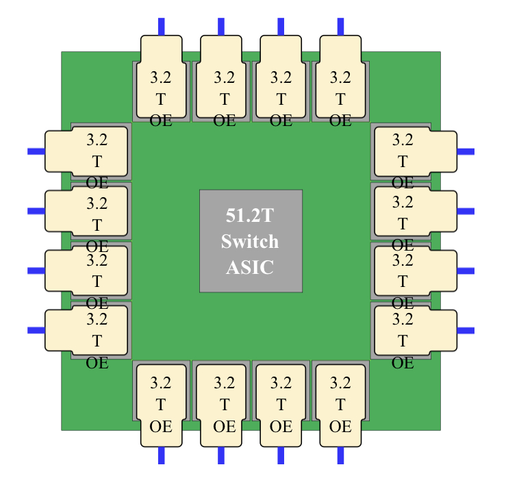
Near package optics tackles this by using a high-performance PCB substrate – an interposer – that sits on the host board, in contrast to co-packaged optics where the modules surround the chip on a multi-chip module substrate.
The near package optics’ interposer is more spacious, making the signal routing between the chip and optical modules easier while still meeting signal integrity requirements. Using the interposer means the whole PCB doesn’t need upgrading which would be extremely costly.
Some co-packaged optics design will use components from multiple suppliers. One concern is how to service a failed optical engine when testing the design before deployment. “That is one reason why a connector-based solution is being proposed,” says Booth. “And that also impacts the size of the substrate.”

A larger substrate is also needed to support both electrical and optical interfaces from the switch chip.
Platforms will not become all-optical immediately and direct-attached copper cabling will continue to be used in the data centre. However, the issue with electrical signalling, as mentioned, is it needs more space than fibre.
“We are in a transitional phase: we are not 100 per cent optics, we are not 100 per cent electrical anymore,” says Booth. “How do you make that transition and still build these systems?”
Perspectives
Ayar Labs views near package optics as akin to COBO. “It’s an attempt to bring COBO much closer to the ASIC,” says Hugo Saleh, senior vice president of commercial operations and managing director of Ayar Labs U.K.
However, COBO’s president, Booth, stresses that near package optics is different from COBO’s on-board optics work.
“The big difference is that COBO uses a PCB motherboard to do the connection whereas near package optics uses a substrate,” he says. “It is closer than where COBO can go.”
It means that with near package optics, there is no high-speed data bandwidth going through the PCB.
Booth says near package optics came about once it became obvious that the latest 51.2-terabit designs – the silicon, optics and the interfaces between them – cannot fit on even the largest organic substrates.
“It was beyond the current manufacturing capabilities,” says Booth. “That was the feedback that came back to Microsoft and Facebook (Meta) as part of our Joint Development Foundation.”
Near package optics is thus a pragmatic solution to an engineering challenge, says Booth. The larger substrate remains a form of co-packaging but it has been given a distinct name to highlight that it is different to the early-version approach.
Nathan Tracy, TE Connectivity and the OIF’s vice president of marketing, admits he is frustrated that the industry is using two terms since co-packaged optics and near package optics achieve the same thing. “It’s just a slight difference in implementation,” says Tracy.
The OIF is an industry forum studying the applications and technology issues of co-packaging and this month published its framework Implementation Agreement (IA) document.
COBO is another organisation working on specifications for co-packaged optics, focussing on connectivity issues.
Technical differences
Ayar Labs highlights the power penalty using near package optics due to its use of longer channel lengths.
For near package optics, lengths between the ASIC and optics can be up to 150mm with the channel loss constrained to 13dB. This is why the OIF is developing the XSR+ electrical interface, to expand the XSR’s reach for near package optics.
In contrast, co-packaged optics confines the modules and host ASIC to 50mm of each other. “The channel loss here is limited to 10dB,” says Nguyen. Co-packaged optics has a lower power consumption because of the shorter spans and 3dB saving.
Ayar Labs highlights its optical engine technology, the TeraPHY chiplet that combines silicon photonics and electronics in one die. The optical module surrounding the ASIC in a co-packaged design typically comprises three chips: the DSP, electrical interface and photonics.
“We can place the chiplet very close to the ASIC,” says Nguyen. The distance between the ASIC and the chiplet can be as close as 3-5mm. Whether on the same interposer Ayar Labs refers to such a design using athird term: in-package optics.
Ayar Labs says its chiplet can also be used for optical modules as part of a co-packaged design.
The very short distances using the chiplet result in a power efficiency of 5pJ/bit whereas that of an optical module is 15pJ/bit. Using TeraPHY for an optical module co-packaged design, the power efficiency is some 7.5pJ/bit, half that of a 3-chip module.
A 3-5mm distance also reduces the latency while the bandwidth density of the chiplet, measured in Gigabit/s/mm, is higher than the optical module.
Co-existence
Booth refers to near package optics as ‘CPO Gen-1’, the first generation of co-packaged optics.
“In essence, you have got to use technologies you have in hand to be able to build something,” says Booth. “Especially in the timeline that we want to demonstrate the technology.”
Is Microsoft backing near package optics?

“We are definitely saying yes if this is what it takes to get the first level of specifications developed,” says Booth.
But that does not mean the first products will be exclusively near package optics.
“Both will be available and around the same time,” says Booth. “There will be near packaged optics solutions that will be multi-vendor and there will be more vertically-integrated designs; like Broadcom, Intel and others can do.”
From an end-user perspective, a multi-vendor capability is desirable, says Booth.
Ayar Labs’ Saleh sees two developing paths.
The first is optical I/O to connect chips in a mesh or as part of memory semantic designs used for high-performance computing and machine learning. Here, the highest bandwidth and lowest power are key design goals.
Ayar Labs has just announced a strategic partnership with high performance computing leader, HPE, to design future silicon photonics solutions for HPE’s Slingshot interconnect that is used for upcoming Exascale supercomputers and also in the data centre.
The second path concerns Ethernet switch chips and here Saleh expects both solutions to co-exist: near package optics will be an interim solution with co-packaged optics dominating longer term. “This will move more slowly as there needs to be interoperability and a wide set of suppliers,” says Saleh.
Booth expects continual design improvements to co-packaged optics. Further out, 2.5D and 3D chip packaging techniques, where silicon is stacked vertically, to be used as part of co-packaged optics designs, he says.

Open Eye gets webscale attention
Microsoft has trialled optical modules that use signalling technology developed by the Open Eye Consortium.
The webscale player says optical modules using the Open Eye’s analogue 4-level pulse-amplitude modulation (PAM-4) technology consume less power than modules with a PAM-4 digital signal processor (DSP).

Brad Booth
“Open Eye has shown us at least an ability that we can do better on power,” says Brad Booth, director, next cloud system architecture, Azure hardware systems and infrastructure at Microsoft, during an Open Eye webinar.
Optical module power consumption is a key element of the total power budget of data centres that can have as many as 100,000 servers and 50,000 switches.
“You want to avoid running past your limit because then you have to build another data centre,” says Booth.
But challenges remain before Open Eye becomes a mainstream technology, says Dale Murray, principal analyst at market research firm, LightCounting.
Open Eye MSA
When the IEEE standards body developed specifications using 50-gigabit PAM-4 optical signals, the assumption was that a DSP would be needed for signal recovery given the optics’ limited bandwidth.
But as optics improved, companies wondered if analogue circuitry could be used after all.
Such PAM-4 analogue chips would be similar to non-return-to-zero (NRZ) signalling chips used in modules, as would the chip assembly and testing, says Timothy Vang, vice president of marketing and applications, signal integrity products group, Semtech. The analogue chips also promised to be cheaper than DSPs.
This led to the formation of the Open Eye multi-source agreement (MSA) in January 2019. Led by MACOM and Semtech, the MSA now has 37 member companies.
“We felt that if we could enable that capability, you could use the same low-cost optics and, with an Open Eye specification - an eye-mask specification - you get a manufacturable low-cost ecosystem,” says Vang. “That was our goal and we were not alone.”
But a key issue is whether Open Eye solutions will work with existing DSP-based PAM-4 modules that have their own testing procedure.
“Can they eliminate all concerns for interoperability between analogue and DSP based modules without dual testing?” says Murray. “And will end users go with a non-standard solution rather than an IEEE-standard solution?”
“We do face the dilemma LightCounting points out,” says Vang. “It is possible there are poor or older DSP-based modules that wouldn’t pass the Open Eye test, and that could lead data centres to say: ‘Well, that is not good enough’.”

Dale Murray
“It is a concern,” says Microsoft’s Booth. The first Open Eye samples Microsoft received didn't talk to all the DSP-based modules, he says, but the next revision appeared to address the issue.
“Digital interfaces are certainly easier, but we're burning a lot of power with the DSPs, in the modules and the switch ASIC,” says Booth. “The switch ASIC needs it for direct attach copper (DAC) cables.”
However, the MSA believes that the cost, power and latency advantages of the Open Eye ICs will prove decisive.
Data centre considerations
Microsoft’s Booth outlined the challenges data centre operators face as bandwidth requirements grow exponentially.
The drivers for greater bandwidth include more home-workers using cloud services during the Covid-19 pandemic and the adoption of artificial intelligence and machine learning.
“With machine learning, the more machines you have talking to each other, the more intensive jobs you can handle,” says Booth. “But for distances greater than a few meters you fall into the realm of the 100m range, and that drives you to an optical solution.”
But optics are costly while going from 100-gigabit to 400-gigabit optical modules has not reduced power consumption. Booth says 400-gigabit SR8 modules consume about 10W while the 400-gigabit DR4 and FR4, it is 12W. Yet for 100-gigabit modules the power consumed is a quarter of these figures.
Low latency is another requirement if data centres are to adopt disaggregated servers where memory is pooled and shared between platforms. “Adding latency to these links, which are fairly short, is an impediment to do this disaggregation scenario,” says Booth.
Microsoft trialled an eight-lane on-board optics COBO module using Open-Eye and achieved a 30 per cent power saving compared to QSFP-DD or OSFP DSP-based pluggable modules.
Open Eye technology could also be used for co-packaged optics, promising a further 10 per cent power saving, says Booth.
Given future 51.2-terabit and 102.4-terabit switch silicon, with their significant connectivity, this will help reduce the overall thermal load and hence cooling which is part of a data centre’s overall power consumption.
“Anything that keeps that heat lower as I increase the bandwidth is an advantage,” says Booth.
Cost, power and latency
The Open Eye MSA claims it will cost a company $80 million to develop a next-generation 5nm CMOS PAM-4 DSP. Such a hefty development cost will need to be recouped, adding to a module's price.
Semtech says its Open Eye analogue ICs use a BiCMOS process which is a far cheaper approach.

Timothy Vang
The PAM-4 DSPs may consume more power, says Vang, but that will improve with newer CMOS processes. First-generation DSPs were implement using 16nm CMOS while the latest devices are at 7nm CMOS.
So the power advantage of Open Eye devices will shrink, says Vang, although Semtech claims its second-generation Open Eye devices will reduce power by 20 per cent.
Open Eye also has a latency advantage. Citing analysis from Nvidia (Mellanox), a PAM-4 DSP-based optical module adds 100ns of latency per link.
In a multi-hop network linking servers, the optical modules account for 40 per cent of the total latency, the rest being the switch, the network interface card and the optical flight time. Using Open Eye-based modules, the optical module portion shrinks to eight per cent only.
Specification status
The Open Eye MSA has specified 53-gigabit PAM-4 signalling for long-reach and short-reach optical links.
In particular, to its 200-gigabit FR4 specification, the MSA is adding 50-gigabit LR1, while an ER1 lite and 200-gigabit LR4 will be completed in early 2021. Meanwhile, the multi-mode 50-gigabit SR1, 200-gigabit SR4 and 400-gigabit SR8 specifications are done.
The third phase of the Open Eye work, producing a 100-gigabit PAM-4 specification, is starting now. Achieving the specification is important for Open Eye since modules are moving to 100-gigabit PAM-4, says Murray.

A 200-gigabit QSFP56-FR4 module block diagram. Source: CIG.
Products
Semtech is already selling 200-gigabit Open Eye short-reach chips, part of its Tri-Edge family. The two 4x50-gigabit devices are dubbed the GN2558 and GN2559.
The GN2558 is the transmitter chip. It retimes four 50-gigabit signals from the host and feeds them to the integrated VCSEL drivers that generate the optical PAM-4 signals sent over four fibres. The four photo-detector outputs are the receiver are then fed to the GN2559 that includes trans-impedance amplifiers (TIAs) and clock data recovery.
Equalisation is used within both devices. “The eye is opened on the transmitter as well as on the receiver; they equalise the signal in each direction,” says Vang.
The Semtech devices are being used for a 200-gigabit SR4 module and for a 400-gigabit SR8 active optical cable where two pairs of each chip are used.
Semtech will launch Tri-Edge long-reach Open Eye chips. The chips will drive externally-modulated lasers (EMLs), directly- modulated lasers (DMLs) and silicon photonics-based designs for single-mode fibre applications.
“We have early versions of these chips sampled and demonstrated,” says Vang. “In the Open Eye MSA, we have shown the chips interoperating with, for example, MACOM’s chipset.”
Semtech’s Tri-Edge solutions are in designs with over two dozen module customers, says Vang.
Meanwhile, pluggable module maker CIG detailed a 200-gigabit QSFP56-FR4 while Optomind discussed a 400-gigabit QSFP56-DD active optical cable design as part of the Open Eye webinar.
COBO issues industry’s first on-board optics specification
- COBO modules supports 400-gigabit and 800-gigabit data rates
- Two electrical interfaces have been specified: 8 and 16 lanes of 50-gigabit PAM-4 signals.
- There are three module classes to support designs ranging from client-slide multi-mode to line-side coherent optics.
- COBO on-board optics will be able to support 800 gigabits and 1.6 terabits once 100-gigabit PAM-4 electrical signals are specified.
 Source: COBO
Interoperable on-board optics has moved a step closer with the publication of the industry’s first specification by the Consortium for On-Board Optics (COBO).
COBO has specified modules capable of 400-gigabits and 800-gigabits rates. The designs will also support 800-gigabit and 1.6-terabit rates with the advent of 100-gigabit single-lane electrical signals.
“Four hundred gigabits can be solved using pluggable optics,” says Brad Booth, chair of COBO and principal network architect for Microsoft’s Azure Infrastructure. “But if I have to solve 1.6 terabits in a module, there is nothing out there but COBO, and we are ready.”
Origins
COBO was established three years ago to create a common specification for optics that reside on the motherboard. On-board optics is not a new technology but until now designs have been proprietary.
I have to solve 1.6 terabits in a module, there is nothing out there but COBO, and we are ready
 Brad BoothSuch optics are needed to help address platform design challenges caused by continual traffic growth.
Getting data on and off switch chips that are doubling in capacity every two to three years is one such challenge. The input-output (I/O) circuitry of such chips consumes significant power and takes up valuable chip area.
There are also systems challenges such as routing the high-speed signals from the chip to the pluggable optics on the platform’s faceplate. The pluggable modules also occupy much of the faceplate area and that impedes the air flow needed to cool the platform.
Using optics on the motherboard next to the chip instead of pluggables reduces the power consumed by shortening the electrical traces linking the two. Fibre rather than electrical signals then carries the data to the faceplate, benefiting signal integrity and freeing faceplate area for the cooling.
Specification 1.0
COBO has specified two high-speed electrical interfaces. One is 8-lanes wide, each lane being a 50-gigabit 4-level pulse-amplitude modulation (PAM-4) signal. The interface is based on the IEEE’s 400GAUI-8, the eight-lane electrical specification developed for 400 Gigabit Ethernet.
The second electrical interface is a 16-lane version for an 800-gigabit module. Using a 16-lane design reduces packaging costs by creating an 800-gigabit module instead using two separate 400-gigabit ones. Heat management is also simpler with one module.
There are also systems benefits using an 800-gigabit module.“As we go to higher and higher switch silicon bandwidths, I don’t have to populate as many modules on the motherboard,” says Booth.
The latest switch chips announced by several companies have 12.8 terabits of capacity that will require 32, 400-gigabit on-board modules but only 16, 800-gigabit ones. Fewer modules simplify the board’s wiring and the fibre cabling to the faceplate.
Designers have a choice of optical formats using the wider-lane module, such as 8x100 gigabits, 2x400 gigabits, and even 800 gigabits.
COBO has tested its design and shown it can support a 100-gigabit electrical interface. The design uses the same connector as the OSFP pluggable module.
“In essence, with an 8-lane width, we could support an 800-gigabit module if that is what the IEEE decides to do next,” says Booth. “We could also support 1.6 terabits if that is the next speed hop.”
It is very hard to move people from their standard operating model to something else until there is an extreme pain point
Form factor and module classes
The approach chosen by COBO differs from proprietary on-board optics designs in that the optics is not mounted directly onto the board. Instead, the COBO module resembles a pluggable in that once placed onto the board, it slides horizontally to connect to the electrical interface (see diagram, top).
A second connector in the middle of the COBO module houses the power, ground and control signals. Separating these signals from the high-speed interface reduces the noise on the data signals. In turn, the two connectors act as pillars supporting the module.
The robust design allows the modules to be mounted at the factory such that the platform is ready for operation once delivered at a site, says Booth.
COBO has defined three module classes that differ in length. The shortest Class A modules are used for 400-gigabit multi-mode interfaces while Class B suits higher-power IEEE interfaces such as 400GBASE-DR4 and the 100G Lambda MSA’s 400G-FR4.
The largest Class C module is for the most demanding and power-hungry designs such as the coherent 400ZR standard. “Class C will be able to handle all the necessary components - the optics and the DSP - associated with that [coherent design],” says Booth.
The advantage of the on-board optics is that it is not confined to a cage as pluggables are. “With an on-board optical module, you can control the heat dissipation by the height of the heat sink,” says Booth. “The modules sit flatter to the board and we can put larger heat sinks onto these devices.”
We realised we needed something as a stepping stone [between pluggables and co-packaged optics] and that is where COBO sits
Next steps
COBO will develop compliance-testing boards so that companies developing COBO modules can verify their designs. Booth hopes that by the ECOC 2018 show to be held in September, companies will be able to demonstrate COBO-based switches and even modules.
COBO will also embrace 100-gigabit electrical work being undertaken by the OIF and the IEEE to determine what needs to be done to support 8-lane and 16-lane designs. For example, whether the forward-error correction needs to be modified or whether existing codes are sufficient.
Booth admits that the industry remains rooted to using pluggables, while the move to co-packaged optics, where the optics and the chip are combined in the same module - remains a significant hurdle, both in terms of packaging technology and the need for vendors to change their business models to build such designs.
“It is very hard to move people from their standard operating model to something else until there is an extreme pain point,” says Booth.
Setting up COBO followed the realisation that a point would be reached when faceplate pluggables would no longer meet demands while in-packaged technology would not be ready.
“We realised we needed something as a stepping stone and that is where COBO sits,” says Booth.
Further information
For information on the COBO specification, click here.
COBO targets year-end to complete specification
Part 3: 400-gigabit on-board optics
- COBO will support 400-gigabit and 800-gigabit interfaces
- Three classes of module have been defined, the largest supporting at least 17.5W
The Consortium for On-board Optics (COBO) is scheduled to complete its module specification this year.
A draft specification defining the mechanical aspects of the embedded optics - the dimensions, connector and electrical interface - is already being reviewed by the consortium’s members.
 Brad Booth“The draft specification encompasses what we will do inside the data centre and what will work for the coherent market,” says Brad Booth, chair of COBO and principal network architect for Microsoft’s Azure Infrastructure.
COBO was established in 2015 to create an embedded optics multi-source agreement (MSA). On-board optics have long been available but until now these have been proprietary solutions.
“Our goal [with COBO] was to get past that proprietary aspect,” says Booth. “That is its true value - it can be used for optical backplane or for optical interconnect and now designers will have a standard to build to.”
The draft specification encompasses what we will do inside the data centre and what will work for the coherent market
Specification
The COBO modules are designed to be interchangeable. Unlike front-panel optical modules, the COBO modules are not ‘hot-pluggable’ - they cannot be replaced while the card is powered. But the design allows for COBO modules to be interchanged.
The COBO design supports 400-gigabit multi-mode and single-mode optical interfaces. The electrical interface chosen is the IEEE-defined CDAUI-8, eight lanes each at 50 gigabits implemented using a 25-gigabit symbol rate and 4-level pulse-amplitude modulation (PAM-4). COBO also supports an 800-gigabit interface using two tightly-coupled COBO modules.
The consortium has defined three module categories that vary in length. The module classes reflect the power envelope requirements; the shortest module supports multi-mode and the lower-power module designs while the longest format supports coherent designs. “The beauty of COBO is that the connectors and the connector spacings are the same no matter what length [of module] you use,” says Booth.
The COBO module is described as table-like, a very small printed circuit board that sits on two connectors. One connector is for the high-speed signals and the other for the power and control signals. “You don't have to have the cage [of a pluggable module] to hold it because of the two-structure support,” says Booth.
To be able to interchange classes of module, a ‘keep-out’ area is used. This area refers to board space that is deliberately left empty to ensure the largest COBO module form factor will fit. A module is inserted onto the board by first pushing it downwards and then sliding it along the board to fit the connection.
Booth points out that module failures are typically due to the optical and electrical connections rather than the optics itself. This is why the repeated accuracy of pick-and-place machines are favoured for the module’s insertion. “The thing you want to avoid is having touch points in the field,” he says.
Coherent
A working group was set up after the Consortium first started to investigate using the MSA for coherent interfaces. This work has now been included in the draft specification. “We realised that leaving it [the coherent work] out was going to be a mistake,” says Booth.
The main coherent application envisaged is the 400ZR specification being developed by the Optical Internetworking Forum (OIF).
The OIF 400ZR interface is the result of Microsoft’s own Madison project specification work. Microsoft went to the industry with several module requirements for metro and data centre interconnect applications.
Madison 1.0 was a two-wavelength 100-gigabit module using PAM-4 that resulted in Inphi’s 80km ColorZ module that supports up to 4 terabits over a fibre. Madison 1.5 defines a single-wavelength 100-gigabit module to support 6.4 to 7.2 terabits on a fibre. “Madison 1.5 is probably not going to happen,” says Booth. “We have left it to the industry to see if they want to build it and we have not had anyone come forward yet.”
Madison 2.0 specified a 400-gigabit coherent-based design to support a total capacity of 38.4 terabits - 96 wavelengths of 400 gigabits.
Microsoft initially envisioned a 43 gigabaud 64-QAM module. However, the OIF's 400ZR project has since adopted a 60-gigabaud 16-QAM module which will achieve either 48 wavelengths at 100GHz spacing or 64 wavelengths at 75GHz spacing, capacities of 19.2Tbps and 25.6Tbps, respectively.
In 2017, the number of coherent metro links Microsoft will use will be 10x greater than the number of metro and long-haul coherent links it used in 2016.
Once Microsoft starting talking about Madison 2.0, other large internet content providers came forward saying they had similar requirements which led to the initiative being driven into the OIF. The result is the 400ZR MSA that the large-scale data centre players want to be built by as many module companies as possible.
Booth highlights the difference in Microsoft’s coherent interface volume requirements just in the last year. In 2017, the number of coherent metro links Microsoft will use will be 10x greater than the number of metro and long-haul coherent links it used in 2016.
“Because it is an order of magnitude more, we need to have some level of specification, some level of interop because now we're getting to the point where if I have an issue with any single supplier, I do not want my business impeded by it,” he says.
Regarding the COBO module, Booth stresses that it will be the optical designers that will determine the different coherent specifications possible. Thermal simulation work already shows that the module will support 17.5W and maybe more.
“There is a lot more capability in this module that there is in a standard pluggable only because we don't have the constraint of a cage,” says Booth. “We can always go up in height and we can always add more heat sink.”
Booth says the COBO specification will likely need a couple more members’ reviews before its completion. “Our target is still to have this done by the end of the year,” he says.
Amended on Sept 4th, added comment about the 400ZR wavelength plans and capacity options
COBO: specification work nearing completion
The Consortium for On-board Optics (COBO) is on target to complete its specifications work by the year end. The work will then enter a final approval stage that will take up to a further three months.

On-board optics, also known as mid-board or embedded optics, have been available for years but vendors have so far had to use custom products. The goal of COBO, first announced in March 2015 and backed by such companies as Microsoft, Cisco Systems, Finisar and Intel, is to develop a technology roadmap and common specifications for on-board optics to ensure interoperability.
Brad Booth (pictured), the chair of COBO and principal architect for Microsoft’s Azure Global Networking Services, says that bringing optics inside systems raises a different set of issues compared to pluggable optical modules used on the front panel of equipment. “If you have a requirement for 32 ports on a faceplate, you know mechanically what you can build,” says Booth.
With on-board optics, the focus is less about size considerations and more about the optical design itself and what is needed to make it work. There is also more scope to future-proof the design, something that can not be done so much with pluggable optics, says Booth.
COBO is working on a 400-gigabit optical module based on the 8-by–50 gigabit interface. The focus in recent months has been on defining the electrical connector that will be needed. The group has narrowed down the choice of candidates to two and the final selection will be based on the connector's signal integrity performance and manufacturability. Also being addressed is how two such modules could be placed side-by-side to create an 800-gigabit (16-by–50 gigabit) design.
COBO’s 400-gigabit on-board optics will support multi-mode and single-mode fibre variants. “When we do a comparison with what the pluggable people are pushing, there are a lot of pluggables that won’t be able to handle the power envelope,” says Booth.
There is no revolutionary change that goes on with technology, it all has to be evolutionary
On-board optics differs from a pluggable module in that the optics and electronics are not confined within a mechanical enclosure and therefore power dissipation is less of an design issue. But by supporting different fibre requirements and reaches new design issues arise. For example, when building a 16-by–50 gigabit design, the footprint is doubled and COBO is looking to eliminate the gap between the two such that a module can be plugged in that is either 8- or 16-lanes wide.
COBO is also being approached about supporting other requirements such as coherent optics for long-distance transmission. A Coherent Working Group has been formed and will meet for the first time in December in Santa Barbara, California. Using on-board optics for coherent avoids the power constraint issues associated with using a caged pluggable module.
On-board optics versus co-packaging
On-board optics is seen as the next step in the evolution of optics as it moves from the faceplate onto the board, closer to the ASIC. There is only so many modules that can fit on a faceplate. The power consumption also raises as the data rate of a pluggable modules increases, as does the power associated with driving faster electrical traces across the board.
Using on-board optics shortens the trace lengths by placing the optics closer to the chip. The board input-output capacity that can be supported also increases as it is fibres not pluggable optics that reside on the front panel. Ultimately, however, designers are already exploring the combining of optics and the chip using a system-in-package design, also known as 2.5D or 3D chip packaging.
Booth says discussions have already taken place between COBO members about co-packaged optics. But he does not expect system vendors to stay with pluggable optics and migrate directly to co-packaging thereby ignoring the on-board optics stage.
“There is no revolutionary change that goes on with technology, it all has to be evolutionary,” says Booth, who sees on-board optics as the next needed transition after pluggables. “You have to have some pathway to learn and discover, and figure out the pain points,” he says. “We are going to learn a lot when we start the deployment of COBO-based modules.”
Booth also sees on-board optics as the next step in terms of flexibility.
When pluggable modules were first introduced they were promoted as allowing switch vendors to support different fibre and copper interfaces on their platforms. The requirements of the cloud providers has changed that broad thinking, he says: “We don’t need that same level of flexibility but there is still a need for suporting different styles of optical interfaces on a switch.”
There are not a lot of other modules that can do 600 gigabit but guess what? COBO can
For example, one data centre operator may favour a parallel fibre solution based on the 100-gigabit PSM4 module while another may want a 100-gigabit wavelength-division multiplexing (WDM) solution and use the CWDM4 module. “This [parallel lane versus WDM] is something embedded optics can cater for,” says Booth.
Moving to a co-packaged design offers no such flexibility. What can a data centre manager do when deciding to change from parallel single-mode optics to wavelength-division multiplexing when the optics is already co-packaged with the chip? “Also how do I deal with an optics failure? Do I have to replace the whole switch silicon?” says Booth. We may be getting to the point where we can embed optics with silicon but what is needed is a lot more work, a lot more consideration and a lot more time, says Booth.
Status
COBO members are busy working on the 400-gigabit embedded module, and by extension the 800-gigabit design. There is also ongoing work as to how to support technologies such as the OIF’s FlexEthernet. Coherent designs will soon support rates such as 600-gigabit using a symbol rate of 64 gigabaud and advanced modulation. “There are not a lot of other modules that can do 600 gigabits but guess what? COBO can,” says Booth.
The good thing is that whether it is coherent, Ethernet or other technologies, all the members are sitting in the same room, says Booth: “It doesn’t matter which market gets there first, we are going to have to figure it out.”
Story updated on October 27th regarding the connector selection and the Coherent Working Group.
COBO looks inside and beyond the data centre
The Consortium of On-Board Optics is working on 400 gigabit optics for the data centre and also for longer-distance links. COBO is a Microsoft-led initiative tasked with standardising a form factor for embedded optics.
Established in March 2015, the consortium already has over 50 members and expects to have early specifications next year and first hardware by late 2017.
 Brad Booth
Brad Booth, the chair of COBO and principal architect for Microsoft’s Azure Global Networking Services, says Microsoft plans to deploy 100 gigabit in its data centres next year and that when the company started looking at 400 gigabit, it became concerned about the size of the proposed pluggable modules, and the interface speeds needed between the switch silicon and the pluggable module.
“What jumped out at us is that we might be running into an issue here,” says Booth.
This led Microsoft to create the COBO industry consortium to look at moving optics onto the line card and away from the equipment’s face plate. Such embedded designs are already being used for high-performance computing, says Booth, while data centre switch vendors have done development work using the technology.
On-board optics delivers higher interface densities, and in many cases in the data centre, a pluggable module isn’t required. “We generally know the type of interconnect we are using, it is pretty structured,” says Booth. But the issue with on-board optics is that existing designs are proprietary; no standardised form factor exists.
“It occurred to us that maybe this is the problem that needs to be solved to create better equipment,” says Booth. Can the power consumed between switch silicon and the module be reduced? And can the interface be simplified by eliminating components such as re-timers?
“This is worth doing if you believe that in the long run - not the next five years, but maybe ten years out - optics needs to be really close to the chip, or potentially on-chip,” says Booth.
400 gigabit
COBO sees 400 gigabit as a crunch point. For 100 gigabit interconnect, the market is already well served by various standards and multi-source agreements so it makes no sense for COBO to go head-to-head here. But should COBO prove successful at 400 gigabit, Booth envisages the specification also being used for 100, 50, 25 and even 10 gigabit links, as well as future speeds beyond 400 gigabit.
The consortium is developing standardised footprints for the on-board optics. “If I want to deploy 100 gigabit, that footprint will be common no matter what the reach you are achieving with it,” says Booth. “And if I want a 400 gigabit module, it may be a slightly larger footprint because it has more pins but all the 400 gigabit modules would have a similar footprint.”
COBO plans to use existing interfaces defined by the industry. “We are also looking at other IEEE standards for optical interfaces and various multi-source agreements as necessary,” says Booth. COBO is also technology agnostic; companies will decide which technologies they use to implement the embedded optics for the different speeds and reaches.
“This is worth doing if you believe that in the long run - not the next five years, but maybe ten years out - optics needs to be really close to the chip, or potentially on-chip."
Reliability
Another issue the consortium is focussing on the reliability of on-board optics and whether to use socketed optics or solder the module onto the board. This is an important consideration given that is it is the vendor’s responsibility to fix or replace a card should a module fail.
This has led COBO to analyse the causes of module failure. Largely, it is not the optics but the connections that are the cause. It can be poor alignment with the electrical connector or the cleanliness of the optical connection, whether a pigtail or the connectors linking the embedded module to the face plate. “The discussions are getting to the point where the system reliability is at a level that you have with pluggables, if not better,” says Booth.
Dropping below $1-per-gigabit
COBO expects the cost of its optical interconnect to go below the $1-per-gigabit industry target. “The group will focus on 400 gigabit with the perception that the module could be four modules on 100 gigabit in the same footprint,” says Booth. Using four 100 gigabit optics in one module saves on packaging and the printed circuit board traces needed.
Booth says that 100 gigabit optics is currently priced between $2 and $3-per-gigabit. “If I integrate that into a 400 gigabit module, the price-per-gig comes down significantly” says Booth. “All the stuff I had to replicate four times suddenly is integrated into one, cutting costs significantly in a number of areas.” Significantly enough to dip below the $1-per-gigabit, he says.
Power consumption and line-side optics
COBO has not specified power targets for the embedded optics in part because it has greater control of the thermal environment compared to a pluggable module where the optics is encased in a cage. “By working in the vertical dimension, we can get creative in how we build the heatsink,” says Booth. “We can use the same footprint no matter whether it is 100 gigabit inside or 100 gigabit outside the data centre, the only difference is I’ve got different thermal classifications, a different way to dissipate that power.”
The consortium is investigating whether its embedded optics can support 100 gigabit long-haul optics, given such optics has traditionally been implemented as an embedded design. “Bringing COBO back to that market is extremely powerful because you can better manage the thermal environment,” says Booth. And by removing the power-hungry modules away from the face plate, surface area is freed up that can be used for venting and improving air flow.
“We should be considering everything is possible, although we may not write the specification on Day One,” says Booth. “I’m hoping we may eventually be able to place coherent devices right next to the COBO module or potentially the optics and the coherent device built together.
“If you look at the hyper-scale data centre players, we have guys that focus just as much on inside the data centre as they do on how to connect the data centres in within a metro area, national area and then sub-sea,” says Booth. “That is having an impact because when we start looking at what we want to do with those networks, we want to have some level of control on what we are doing there and on the cost.
“We buy gazillions of optical modules for inside the data centre. Why is it that we have to pay exorbitant prices for the ones that we are not using inside [the data centre],” he says.
“I can’t help paint a more rosier picture because when you have got 1.4 million servers, if I end up with optics down to all of those, that is a lot of interconnect“
Market opportunities
Having a common form factor for on-board optics will allow vendors to focus on what they do best: the optics. “We are buying you for the optics, we are not buying you for the footprint you have on the board,” he says.
Booth is sensitive to the reservations of optical component makers to such internet business-led initiatives. “It is a very tough for these guys to extend themselves to do this type of work because they are putting a lot of their own IP on the line,” says Booth. “This is a very competitive space.”
But he stresses it is also fiercely competitive between the large internet businesses building data centres. “Let’s sit down and figure out what does it take to progress this industry. What does it take to make optics go everywhere?”
Booth also stresses the promising market opportunities COBO can serve such as server interconnect.
“When I look at this market, we are talking about doing optics down to our servers,” says Booth. “I can’t help paint a more rosier picture because when you have got 1.4 million servers, if I end up with optics down to all of those, that is a lot of interconnect.“