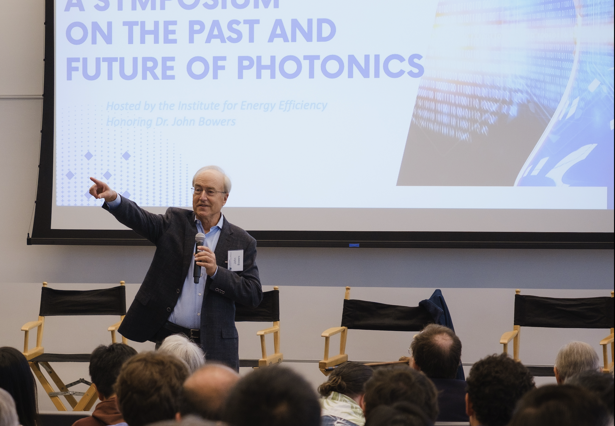
John Bowers: We are still at the dawn of photonics
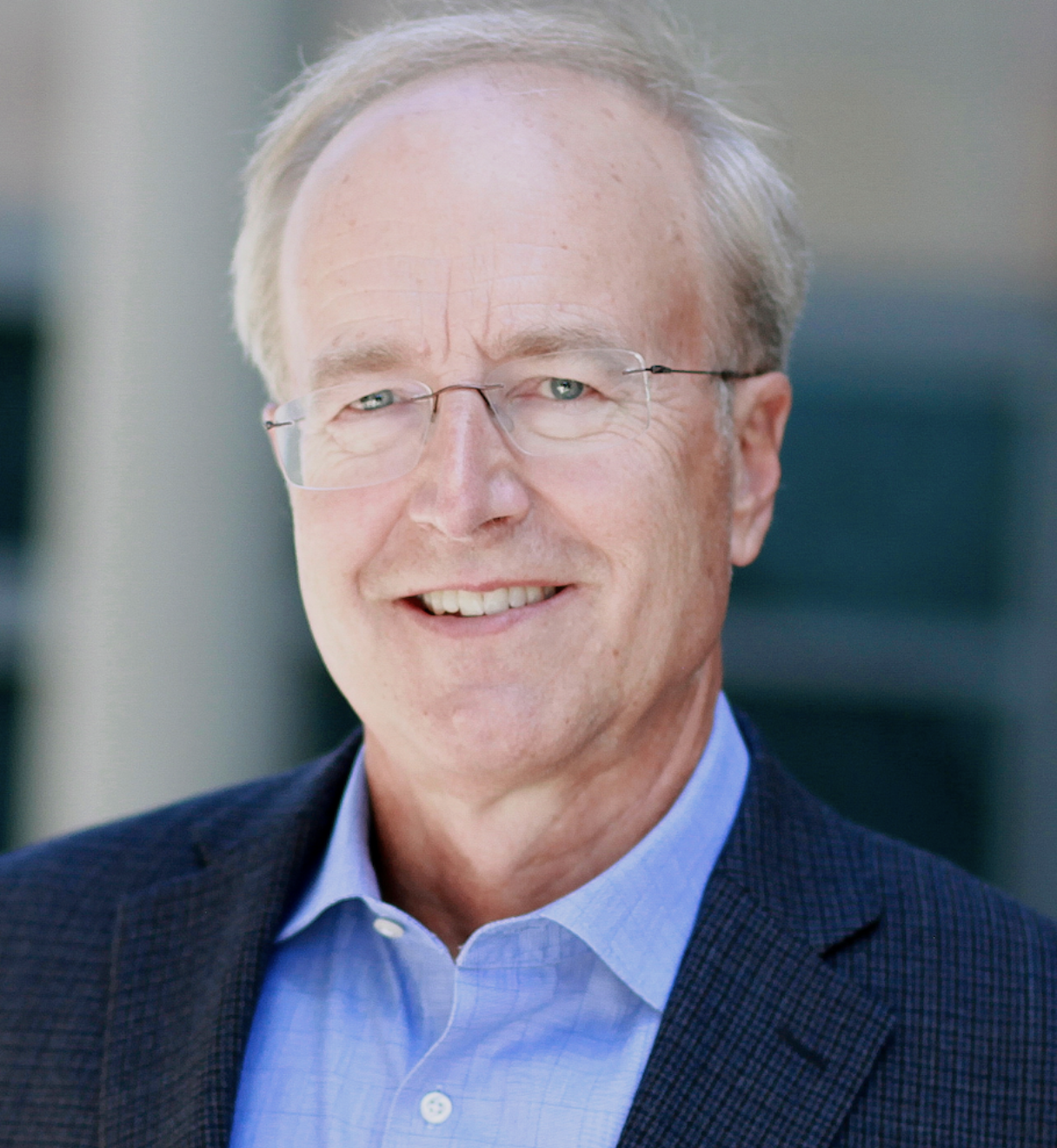
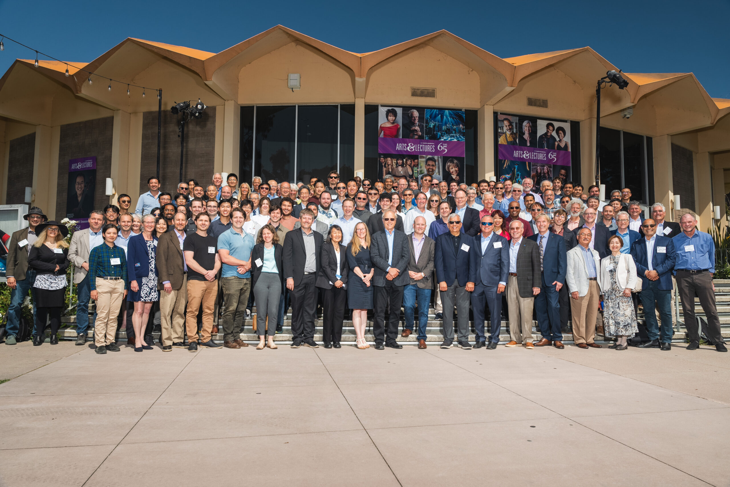
After 38 years at the University of California, Santa Barbara (UCSB), Professor John Bowers (pictured) is stepping away from teaching and administrative roles to focus on research.
He welcomes the time it will free for biking and golf. He will also be able to linger, not rush, when travelling. On a recent trip to Saudi Arabia, what would have centered around a day-event became a week-long visit.
Bowers’ career includes significant contributions to laser integration and silicon photonics, mentoring some 85 PhD students, and helping found six start-ups, two of which he was the CEO.
Early Influences
Bowers’ interest in science took root while at high school. He built oscilloscopes and power supplies using Heathkits, then popular educational assemblies for electronics enthusiasts. He was also inspired by his physics and chemistry teachers, subjects he majored in at the University of Minnesota.
A challenging experience led him to focus solely on physics: “I took organic chemistry and hated it,” says Bowers. “I went, ‘Okay, let’s stick to inorganic materials.’”
Bowers became drawn to high-energy physics and worked in a group conducting experiments at Fermilab and Argonne National Laboratories. Late-night shifts – 10 PM to 6 AM – offered hands-on learning, but a turning point came when his mentor was denied tenure. “My white knight fell off his horse,” he says.
He switched to applied physics at Stanford, where he explored gallium arsenide and silicon acoustic devices, working under the supervision of the late Gordon Kino, a leading figure in applied physics and electrical engineering.
Bowers then switched to fibre optics, working in a group that was an early leader in single-mode optical fibre. “It was a period when fibre optics was just taking off,” says Bowers. “In 1978, they did the first 50-megabit transmission system, and OFC [the premier optical fibre conference] was just starting.”
Bell Labs and fibre optics
After gaining his doctorate, Bowers joined Bell Labs, where his work focused on the devices—high-speed lasers and photodetectors—used for fibre transmission. He was part of a team that scaled fibre-optic systems from 2 to 16 gigabits per second. However, the 1984 AT&T breakup signalled funding challenges, with Bell Labs losing two-thirds of its financial support.
Seeking a more stable environment, Bowers joined UCSB in 1987. He was attracted by its expertise in semiconductors and lasers, including the presence of the late Herbert Kroemer, who went on to win the 2000 Nobel Prize in Physics. Kroemer developed the double heterostructure laser and played a big part in enticing Bowers to join. Bowers was tasked with continuing the laser work, something he has done for the last 40 years.
“Coming to Santa Barbara was brilliant, in retrospect,” says Bowers, citing its strong collaborative culture and a then newly formed materials department.
Integrated lasers
At UCSB, Bowers worked on integrated circuits using indium phosphide, including tunable lasers and 3D stacking of photonic devices.
At the same time, the field of silicon photonics was starting after Richard Soref wrote a seminal paper proposing silicon as an optical material for photonic integrated circuits (PIC).
“We all knew that silicon was a terrible light emitter because it is an indirect band-gap material,” says Bowers. “So when people started talking about silicon photonics, I kept thinking: ‘Well, that is fine, but you need a light source, and if you don’t have a light source, it’ll never become important.’”
Bowers tackled integrating lasers onto silicon to address the critical need for an on-chip light source. He partnered with Intel’s Mario Paniccia and his team, which had made tremendous progress developing a silicon Raman lasers with higher powers and narrower linewidths.
“It was very exciting, but you still needed a pump laser; a Raman laser is just a wavelength converter from one wavelength to another,” says Bowers. “So I focused on the pump laser end, and the collaboration benefitted us both.”
Intel commercialised the resulting integrated laser design and sold millions of silicon-photonics-based pluggable transceivers.
“Our original vision was verified: the idea that if you have CMOS processing, the yields will be better, the performance will be better, the cost will be lower, and it scales a lot better,” says Bowers. “All that has proven to be true.
Is Bowers surprised that integrated laser designs are not more widespread?
All the big silicon photonics companies, including foundry TSMC, will incorporate lasers into their products, he says, just as Intel has done and Infinera before that.
Infinera, an indium phosphide photonic integrated circuit (PIC) company now acquired by Nokia, claimed that integration would improve the reliability and lower the cost, says Bowers: “Infinera did prove that with indium phosphide and Intel did the same thing for silicon.”
The indium phosphide transceiver has a typical failure rate of 10 FIT (failures per ten billion hours), and if there are 10 laser devices, the FIT rises to 100, he says. By contrast, Intel’s design has a FIT of 0.1, and so with 10, the FIT becomes on the order of 1.
Silicon lasers are more reliable because there’s no III-V material exposed anywhere. Silicon or silicon dioxide facets eliminate the standard degradation mechanisms in III-V materials. This enables non-hermetic packaging, reducing costs and enabling rapid scaling.
According to Bowers, Intel scaled to a million transceivers in one year. Such rapid scaling to high volumes is important for many applications, and that is where silicon photonics has an advantage.
“Different things motivate different people. For me, it’s not about money, it’s more about your impact, particularly on students and research fields. To the extent that I’ve contributed to silicon photonics becoming important and dynamic, that is something I’m proud of.”
-Professor John Bowers
Optical device trends
Bowers notes how the rise of AI has surprised everyone, not just in terms of the number of accelerator chips needed but their input-output (I/O) requirements.
Copper has been the main transmission medium since the beginning of semiconductor chips, but that is now being displaced by optics – silicon photonics in particular – for the communications needs of very high bandwidth chips. He also cites companies like Broadcom and Nvidia shipping co-packaged optics (CPO) for their switching chips and platforms.
“Optics is the only economic way to proceed, you have to work on 3D stacking of chips coupled with modern packaging techniques,” he says, adding that the need for high yield and high reliability has been driving the work on III-V lasers on silicon.
One current research focus for Bowers is quantum dot lasers, which reduce the line width and minimise reflection sensitivity by 40dB. This eliminates the need for costly isolators in datacom transceivers.
Quantum dot devices also show exceptional durability, with lifetimes for epitaxial lasers on silicon a million times longer than quantum well devices on silicon and 10 times less sensitivity to radiation damage, as shown in a recent Sandia National Labs study for space applications.
Another area of interest is modulators for silicon photonics. Bowers says his group is working on sending data at 400 gigabits-per-wavelength using ‘slow light’ modulators. These optical devices modulate the intensity or phase, of light. Slowing down the light improves its interaction in the material, improving efficiency and reducing device size and capacitance. He sees such modulators is an important innovation.
“Those innovations will keep happening; we’re not limited in terms of speed by the modulator,” says Bowers, who also notes the progress in thin-film lithium niobate modulators, which he sees as benefiting silicon photonics, “We have written papers suggesting most of the devices may be III-V,” says Bowers, and the same applies to materials such as thin-film lithium niobate.
“I believe that as photonic systems become more complex, with more lasers and amplifiers, then everyone will be forced to integrate,” says Bowers.
Other applications
Beyond datacom, Bowers sees silicon photonics enabling LIDAR, medical sensors, and optical clocks. His work on low-noise lasers, coupled to silicon nitride waveguides, reduces phase noise by 60dB, enhancing sensor sensitivity. “If you can reduce the frequency noise by 60dB, then that makes it either 60dB more efficient, or you need 60dB less power,” he says.
Applications include frequency-based sensors for gas detection, rotation sensing, and navigation, where resonance frequency shifts detect environmental changes.
Other emerging applications include optical clocks for precise timing in navigation, replacing quartz oscillators. “You can now make very quiet clocks, and at some point we can integrate all the elements,” Bowers says, envisioning chip-scale solutions.
Mentorship and entrepreneurial contributions
Bowers’ impact extends to mentorship, guiding so many PhD students who have gone on to achieve great success.
“It’s very gratifying to see that progression from an incoming student who doesn’t know what an oscilloscope is to someone who’s running a group of 500 people,” he says.
Alan Liu, former student and now CEO of the quantum dot photonics start-up Quintessent, talks about how Bowers calls on his students to ‘change the world’.
Liu says it is not just about pushing the frontiers of science but also about having a tangible impact on society through technology and entrepreneurship.”
Bowers co-founded UCSB’s Technology Management Department and taught entrepreneurship for 30 years. Drawing on mentors like Milton Chang, he focused on common start-up pitfalls: “Most companies fail for the same set of reasons.”
His own CEO start-up experience informed his teaching, highlighting interdisciplinary skills and team dynamics.
Mario Paniccia, CEO of Anello Photonics, who collaborated with Bowers as part of the Intel integrated laser work, highlights Bowers’ entrepreneurial skills.
“John is one of the few professors who are not only brilliant and technically a world expert – in John’s case, in III-V materials – but also business savvy and entrepreneurial,” says Paniccia. “He is not afraid to take risks and can pick and hire the best.”
Photonics’ future roadmap
Bowers compares photonics’ trajectory to electronics in the 1970s, when competing CMOS technologies standardised, shifting designers’ focus from device development to complex circuits. “Just like in the 1970s, there were 10 competing transistor technologies; the same consolidation will happen in photonics,” he says.
Standardised photonic components will be integrated into process design kits (PDKs), redirecting research toward systems like sensors and optical clocks.
“We’re not at the end, we’re at the beginning of photonics,” emphasises Bowers.
Reflections
Looking back, would he have done anything differently?
A prolonged pause follows: “I’ve been very happy with the choices I have made,” says Bowers, grateful for his time at UCSB and his role in advancing silicon photonics.
Meanwhile, Bowers’ appetite for photonics remains unwavering: “The need for photonic communication, getting down to the chip level, is just going to keep exploding,” he says.

SDM and MIMO: An interview with Bell Labs
Part 2: The capacity crunch and the role of SDM
The argument for spatial-division multiplexing (SDM) - the sending of optical signals down parallel fibre paths, whether multiple modes, cores or fibres - is the coming ‘capacity crunch’. The information-carrying capacity limit of fibre, for so long described as limitless, is being approached due to the continual yearly high growth in IP traffic. But if there is a looming capacity crunch, why are we not hearing about it from the world’s leading telcos?
“It depends on who you talk to,” says Peter Winzer, head of the optical transmission systems and networks research department at Bell Labs. The incumbent telcos have relatively low traffic growth - 20 to 30 percent annually. “I believe fully that it is not a problem for them - they have plenty of fibre and very low growth rates,” he says.
Twenty to 30 percent growth rates can only be described as ‘very low’ when you consider that cable operators are experiencing 60 percent year-on-year traffic growth while it is 80 to 100 percent for the web-scale players. “The whole industry is going through a tremendous shift right now,” says Winzer.
In a recent paper, Winzer and colleague Roland Ryf extrapolate wavelength-division multiplexing (WDM) trends, starting with 100-gigabit interfaces that were adopted in 2010. Assuming an annual traffic growth rate of 40 to 60 percent, 400-gigabit interfaces become required in 2013 to 2014, and the authors point out that 400-gigabit transponder deployments started in 2013. Terabit transponders are forecast in 2016 to 2017 while 10 terabit commercial interfaces are expected from 2020 to 2024.
In turn, while WDM system capacities have scaled a hundredfold since the late 1990s, this will not continue. That is because systems are approaching the Non-linear Shannon Limit which estimates the upper limit capacity of fibre at 75 terabit-per-second.
Starting with 10-terabit-capacity systems in 2010 and a 30 to 40 percent core network traffic annual growth rate, the authors forecast that 40 terabit systems will be required shortly. By 2021, 200 terabit systems will be needed - already exceeding one fibre’s capacity - while petabit-capacity systems will be required by 2028.
Even if I’m off by an order or magnitude, and it is 1000, 100-gigabit lines leaving the data centre; there is no way you can do that with a single WDM system
Parallel spatial paths are the only physical multiplexing dimension remaining to expand capacity, argue the authors, explaining Bell Labs’ interest in spatial-division multiplexing for optical networks.
If the telcos do not require SDM-based systems anytime soon, that is not the case for the web-scale data centre operators. They could deploy SDM as soon as 2018 to 2020, says Winzer.
The web-scale players are talking about 400,000-server data centres in the coming three to five years. “Each server will have a 25-gigabit network interface card and if you assume 10 percent of the traffic leaves the data centre, that is 10,000, 100-gigabit lines,” says Winzer. “Even if I’m off by an order or magnitude, and it is 1000, 100-gigabit lines leaving the data centre; there is no way you can do that with a single WDM system.”
SDM and MIMO
SDM can be implemented in several ways. The simplest way to create parallel transmission paths is to bundle several single-mode fibres in a cable. But speciality fibre can also be used, either multi-core or multi-mode.
For the demo, Bell Labs used such a fibre, a coupled 3-core one, but Sebastian Randel, a member of technical staff, said its SDM receiver could also be used with a fibre supporting a few spatial modes. By increasing slightly the diameter of a single-mode fibre, not only is a single mode supported but two second-order modes. “Our signal processing would cope with that fibre as well,” says Winzer.
The signal processing referred to, that restores the multiple transmissions at the receiver, implements multiple input, multiple output or MIMO. MIMO is a well-known signal processing technique used for wireless and digital subscriber line (DSL).
They are garbled up, that is what the rotation is; undoing the rotation is called MIMO
Multi-mode fibre can support as many as 100 spatial modes. “But then you have a really big challenge to excite all 100 spatial modes individually and detect them individually,” says Randel. In turn, the digital signal processing computation required for the 100 modes is tremendous. “We can’t imagine we can get there anytime soon,” says Randel.
Instead, Bell Labs used 60 km of the 3-core coupled fibre for its real-time SDM demo. The transmission distance could have been much longer except the fibre sample was 60 km long. Bell Labs chose the coupled-core fibre for the real-time MIMO demonstration as it is the most demanding case, says Winzer.
The demonstration can be viewed as an extension of coherent detection used for long-distance 100 gigabit optical transmission. In a polarisation-multiplexed, quadrature phase-shift keying (PM-QPSK) system, coupling occurs between the two light polarisations. This is a 2x2 MIMO system, says Winzer, comprising two inputs and two outputs.
For PM-QPSK, one signal is sent on the x-polarisation and the other on the y-polarisation. The signals travel at different speeds while hugely coupling along the fibre, says Winzer: “The coherent receiver with the 2x2 MIMO processing is able to undo that coupling and undo the different speeds because you selectively excite them with unique signals.” This allows both polarisations to be recovered.
With the 3-core coupled fibre, strong coupling arises between the three signals and their individual two polarisations, resulting in a 6x6 MIMO system (six inputs and six outputs). The transmission rotates the six signals arbitrarily while the receiver, using 6x6 MIMO, rotates them back. “They are garbled up, that is what the rotation is; undoing the rotation is called MIMO.”
Demo details
For the demo, Bell Labs generated 12, 2.5-gigabit signals. These signals are modulated onto an optical carrier at 1550nm using three nested lithium niobate modulators. A ‘photonic lantern’ - an SDM multiplexer - couples the three signals orthogonally into the fibre’s three cores.
The photonic lantern comprises three single-mode fibre inputs fed by the three single-mode PM-QPSK transmitters while its output places the fibres closer and closer until the signals overlap. “The lantern combines the fibres to create three tiny spots that couple into a single fibre, either single mode or multi-mode,” says Winzer.
At the receiver, another photonic lantern demultiplexes the three signals which are detected using three integrated coherent receivers.
Don’t do MIMO for MIMO’s sake, do MIMO when it helps to bring the overall integrated system cost down
To implement the MIMO, Bell Labs built a 28-layer printed circuit board which connects the three integrated coherent receiver outputs to 12, 5-gigabit-per-second 10-bit analogue-to-digital converters. The result is an 600 gigabit-per-second aggregate output digital data stream. This huge data stream is fed to a Xilinx Virtex-7 XC7V2000T FPGA using 480 parallel lanes, each at 1.25 gigabit-per-second. It is the FPGA that implements the 6x6 MIMO algorithm in real time.
“Computational complexity is certainly one big limitation and that is why we have chosen a relatively low symbol rate - 2.5 Gbaud, ten times less than commercial systems,” says Randel. “But this helps us fit the [MIMO] equaliser into a single FPGA.”
Future work
With the growth in IP traffic, optical engineers are going to have to use space and wavelengths. “But how are you going to slice the pie?” says Winzer.
With the example of 10,000, 100-gigabit wavelengths, will 100 WDM channels be sent over 100 spatial paths or 10 WDM channels over 1,000 spatial paths? “That is a techno-economic design optimisation,” says Winzer. “In those systems, to get the cost-per-bit down, you need integration.”
That is what the Bell Lab’s engineers are working on: optical integration to reduce the overall spatial-division multiplexing system cost. “Integration will happen first across the transponders and amplifiers; fibre will come last,” says Winzer.
Winzer stresses that MIMO-SDM is not primarily about fibre, a point frequently misunderstood. The point is to enable systems with crosstalk, he says.
“So if some modulator manufacturer can build arrays with crosstalk and sell the modulator at half the price they were able to before, then we have done our job,” says Winzer. “Don’t do MIMO for MIMO’s sake, do MIMO when it helps to bring the overall integrated system cost down.”
Further Information:
Space-division Multiplexing: The Future of Fibre-Optics Communications, click here
For Part 1, click here
Bell Labs demos real-time MIMO over multicore fibre
Bell Labs, the research arm of Alcatel-Lucent, has used a real-time receiver to recover a dozen 2.5-gigabit signals sent over a coupled three-core fibre. Until now the signal processing for such spatial-division multiplexed transmissions have been done offline due to the computational complexity involved.
 “The era of real-time experiments in spatial-division multiplexing is starting and this is the very first example” - Peter Winzer
“The era of real-time experiments in spatial-division multiplexing is starting and this is the very first example,” said Peter Winzer, head of the Optical Transmission Systems and Networks Research Department at Bell Labs. “Such real-time experiments are the next stepping stone towards a true product implementation.”
Spatial-division multiplexing promises to increase the capacity of optical fibre by a factor of between ten and one hundredfold. Multiple input, multiple output [MIMO], a signal processing technique employed for wireless and for DSL broadband access, is used to recover the signals at the receiver.
MIMO also promises optical designers a way to tackle crosstalk between components, enabling cheaper integrated optics to be used at the expense of more complex digital signal processing, said Winzer.
For the demo, Bell-Labs used MIMO to recover twelve 2.5-gigabit transmitted signals down a three-core fibre, in effect three polarisation-multiplexed, quadrature phase-shift keying (PM-QPSK) signals. The result is a 6x6 MIMO system [six inputs, six outputs] due to the coupling between the three signals, each with two polarisations. The signal couplings cause an arbitrary rotation in a 6-dimensional space, says Winzer: “They are garbled up, that is what the rotation is. Undoing the rotation is called MIMO.”
The signals were transmitted at 1,550nm over a 60 km spool of coupled-core fibre. The three 10 gigabit PM-QPSK signals are a tenth the speed of commercial systems but this was necessary for an FPGA to execute MIMO in real time.
According to Bell Labs, the coupled-core fibre was chosen for the real-time receiver demonstration as it is the most taxing example. The Bell Labs team is now working on optical integration to reduce the overall spatial-division multiplexing system’s cost-per-bit. “Making those transponders cheaper, we are trying to figure out what are the right knobs to turn,” said Winzer.
Bell Labs does not expect telcos to require spatial-division systems soon. But traffic requirements of the web-scale data centre operators could lead to select deployments in three to five years, said Winzer.
For Part 2, a more detailed discussion with Bell Labs about spatial-division multiplexing and the 60km 6x6 MIMO demonstration, click here
ECOC '15 Reflections: Part 2
Martin Zirngibl, head of network enabling components and technologies at Bell Labs.
Silicon Photonics is seeming to gain traction, but traditional component suppliers are still betting on indium phosphide.
There are many new start-ups in silicon photonics, most seem to be going after the 100 gigabit QSFP28 market. However, silicon photonics still needs a ubiquitous high-volume application for the foundry model to be sustainable.
There is a battle between 4x25 Gig CWDM and 100 Gig PAM-4 56 gigabaud, with most people believing that 400 Gig PAM-4 or discrete multi-tone with 100 Gig per lambda will win.
Will coherent make it into black and white applications - up to 80 km - or is there a role for a low-cost wavelength-division multiplexing (WDM) system with direct detection?
One highlight at ECOC was the 3D integrated 100 Gig silicon photonics by Kaiam.
In coherent, the analogue coherent optics (ACO) model seems to be winning over the digital coherent one, and people are now talking about 400 Gig single carrier for metro and data centre interconnect applications.
As for what I’ll track in the coming year: will coherent make it into black and white applications - up to 80 km - or is there a role for a low-cost wavelength-division multiplexing (WDM) system with direct detection?
Yukiharu Fuse, director, marketing department at Fujitsu Optical Components
There were no real surprises as such at ECOC this year. The products and demonstrations on show were within expectations but perhaps were more realistic than last year’s show.
Most of the optical component suppliers demonstrated support to meet the increasing demand of data centres for optical interfaces.
The CFP2 Analogue Coherent Optics (CFP2-ACO) form factor’s ability to support multiple modulation formats configurable by the user makes it a popular choice for data centre interconnect applications. In particular, by supporting 16-QAM, the CFP2-ACO can double the link capacity using the same optics.
Lithium niobate and indium-phosphide modulators will continue to be needed for coherent optical transmission for years to come
Recent developments in indium phosphide designs has helped realise the compact packaging needed to fit within the CFP2 form factor.
I saw the level of integration and optical engine configurations within the CFP2-ACO differ from vendor to vendor. I’m interested to see which approach ends up being the most economical once volume production starts.
Oclaro introduced a high-bandwidth lithium niobate modulator for single wavelength 400 gigabit optical transmission. Lithium niobate continues to play an important role in enabling future higher baud rate applications with its excellent bandwidth performance. My belief is that both lithium niobate and indium-phosphide modulators will continue to be needed for coherent optical transmission for years to come.
Chris Cole, senior director, transceiver engineering at Finisar
ECOC technical sessions and exhibition used to be dominated by telecom and long haul transport technology. There is a shift to a much greater percentage focused on datacom and data centre technology.
What I learned at the show is that cost pressures are increasing
There were no major surprises at the show. It was interesting to see about half of the exhibition floor occupied by Chinese optics suppliers funded by several Chinese government entities like municipalities jump-starting industrial development.
What I learned at the show is that cost pressures are increasing.
New datacom optics technologies including optical packaging, thermal management, indium phosphide and silicon integration are all on the agenda to track in the coming year.
10 Gigabit Plain Old Telephone Service
Bell Labs has sent unprecedented amounts of data down a telephone wire. The research arm of Alcatel-Lucent has achieved one-gigabit streams in both directions over 70m of wire, and 10-gigabit one-way over 30m using a bonded pair of telephone wires.
 Keith RussellThe demonstrations show how gigabit-speed broadband could use telephone wire to bridge the gap between a local optical fibre point and a home. The optical fibre point may be located at the curbside, on a wall or in an apartment's basement.
Service providers want to deliver gigabit services to compete with cable operators and developments like Google Fiber, the Web giant's one-gigabit broadband initiative in the US. Such technology will help the operators deploy gigabit broadband, saving them time and expense.
"This kind of a technology is really going to be an enabler of fibre-to-the-home," says Keith Russell, senior marketing manager, fixed networks business at Alcatel-Lucent. "Service providers will have another tool, addressing those parts of the network where it is hard to drive fibre right to the home, whether it is a multi-dwelling unit or where they can't trench fibre those last few meters."
Bell Labs delivers gigabits of data down the telephone wire by using more spectrum. VDSL2 uses 17MHz of spectrum while the first implementation of the emerging G.fast standard extends the frequency band to 106MHz. Alcatel-Lucent has gone beyond G.fast and uses even more spectrum: 350MHz for symmetrical 1 Gigabit, and up to 500MHz to demonstrate 10 Gigabit. Bell Labs calls its technology XG-FAST.
BT's chief executive, Gavin Patterson, has already described G.fast as a very exciting technology. "It allows us to get speeds of up to one-gigabit, and it builds on VDSL," said Patterson during BT's most recent quarterly results call. "It takes the fibre closer to the premise, so effectively you get a glass transmission closer to the premise but not always all the way in."
XG-FAST will take longer and will likely be commercially available only from 2018, says Teresa Mastrangelo, principal analyst at Broadbandtrends: "That timeline may still provide a quicker means to deploying gigabit services than having to deploy a full-blown fibre-to-the-home network."
 Source: Alcatel-Lucent Bell Labs
Using such a broad spectrum of the telephone wire, designed a century ago to carry voice signals several kilohertz wide, creates two challenges.
One is that signal attenuation grows with frequency. Hence the wider the spectrum, the shorter the copper loop length over which data can travel. VDSL2 has a loop-length of some 1,500 meters while XG-FAST achieves tens of meters.
The second issue is crosstalk, where the signal on a copper pair leaks into a neighbouring pair, generating electrical noise. The leakage can be so noisy at the higher frequencies that it can exceed the desired signal.
For the Bell Labs demonstration, crosstalk was only an issue in the 10-gigabit example that uses two wire pairs. However, for VDSL2 and for the emerging G.fast standard, crosstalk is a significant problem. Systems vendors have developed advanced digital signal processing techniques, known as vectoring, to reject such noise.
Russell says that the G.fast standard's first phase - based on 106MHz of spectrum - will be ratified by year end. G.fast's second phase proposes doubling the spectrum to 212MHz. Alcatel-Lucent demonstrations using XG-FAST shows that digital subscriber line technology need not stop there.
"A lot of work is needed to take it [XG-FAST] into production," says Russell. First, there are engineering challenges, the broad spectrum used makes the analogue front-end chip design significantly more complex and expensive. Engineering effort will be needed before the cost of such a solution will match that of VDSL.
XG-FAST would also need to be considered along with other proposals and the chosen outcome standardised before operators will embrace the technology in their networks. Meanwhile, operators will start testing G.fast from next year with products appearing mid-2015.
Another issue is the need for extensive copper characterisation in order to understand the state of the copper and whether it can even support this type of technology, says Mastrangelo.
"It will be very interesting to see what happens with G.fast given the operator interest in gigabit services," says Russell. "[G.fast] is a very strong option for operators wanting to offer such services quickly."
BT estimates that the technology is two years away before it will play a role in the network.
* The article was further edited and added to on July 16th.
Books in 2013 - Part 2
Steve Alexander, CTO of Ciena
David and Goliath: Underdogs, Misfits, and the Art of Battling Giants by Malcolm Gladwell.
I’ve enjoyed some of Gladwell’s earlier works such as The Tipping Point and Outliers: The Story of Success. You often have to read his material with a bit of a skeptic's eye since he usually deals with people and events that are at least a standard deviation or two away from whatever is usually termed “normal.” In this case he makes the point that overcoming an adversity (and it can be in many forms) is helpful in achieving extraordinary results. It also reminded me of the many people who were skeptical about Ciena’s initial prospects back in the middle '90s when we first came to market as a “David” in a land of giant competitors. We clearly managed to prosper and have now outlived some of the giants of the day.
Overconnected: The Promise and Threat of the Internet by William Davidow.
I downloaded this to my iPad a while back and finally got to read it on a flight back from South America. On my trip what had I been discussing with customers? Improving network connections of course. I enjoyed it quite a bit because I see some of his observations within my own family. The desire to “connect” whenever something happens and the “positive feedback” that can result from an over-rich set of connections can be both quite amusing as well as a little scary! I don’t believe that all of the events that the author attributes to being overconnected are really as cause-and-effect driven as he may portray, but I found the possibilities for fads, market bubbles, and market collapses entertaining.
For another insight into such extremes see Extraordinary Popular Delusions and the Madness of Crowds by Charles Mackay, first published in the 1840s. We, as a species, have been a bit wacky for a long time.
Shadow Divers: The True Adventure of Two Americans Who Risked Everything to Solve One of the Last Mysteries of World War II by Robert Kurson.
Having grown up in the New York / New Jersey area and having listened to stories from my parents about the fear of sabotage in World War II (Google Operation Pastorius for some background) and grandparents, who had experienced the Black Tom Explosion during WW1, this book was a “don’t put it down till done” for me. I found it by accident when browsing a used book store. It’s available on Kindle and is apparently somewhat controversial because another diver has written a rebuttal to at least some of what was described. It is a great example of what it takes to both dive deep and solve a mystery.
David Welch, President, Infinera
Here is my cut. The first three books offer a perspective on how people think and I apply it to business.
- The Talent Code: Greatness Isn't Born. It's Grown. Here's How by Daniel Coyle.
- Mindset: The New Psychology of Success by Carol Dweck
- Moneyball: The Art of Winning an Unfair Game by Michael Lewis.
My non-work related book is Unbroken: A World War II Story of Survival, Resilience, and Redemption by Laura Hillenbrand.
Unfortunately, I rarely get time to read books, so the picking can be thin at times.
Marcus Weldon, President of Bell Labs and CTO, Alcatel-Lucent
I am currently re-reading Jon Gertner's history of Bell labs, called The Idea Factory: Bell Labs and the Great Age of American Innovation which should be no surprise as I have just inherited the leadership of this phenomenal place, and much of what he observes is still highly relevant today and will inform the future that I am planning.
I joined Bell Labs in 1995 as a post-doctoral researcher in the famous, Nobel-prize winning Physics Division (Div111, as it was known) and so experienced much of this first hand. In particular, I recall being surrounded by the most brilliant, opinionated, odd, inspired, collaborative, competitive, driven, relaxed, set of people I had ever met. And with the shared goal of solving the biggest problems in information and telecommunications.
Having recently returned back to the 'bosom of bell', I find that, remarkably, much of that environment and pool of talent still remains. And that is hugely exciting as it means that we still have the raw ingredients for the next great era of Bell Labs. My hope is that 10 years from now Gertner will write a second edition or updated version of the tale that includes the renewed success of Bell Labs, and not just the historical successes.
On the personal front, I am reading whatever my kids ask me to read them. Two of the current favourites are: Turkey Claus, about a turkey trying to avoid becoming the centrepiece of a Christmas feast by adapting and trying various guises, and Pete the Cat Saves Christmas, about a world of an ailing feline Claus, requiring average cat, Pete, to save the big day.
I am not sure there is a big message here, but perhaps it is that 'any one of us can be called to perform great acts, and can achieve them, and that adaptability is key to success'. And of course, there is some connection in this to the Bell Labs story above, so I will leave it there!
Books in 2013: Part 1, click here
Interview with Finisar's Jerry Rawls
Finisar is celebrating its 25th anniversary. Gazettabyte interviewed Finisar's executive chairman and company co-founder, Jerry Rawls, to mark the anniversary.
Part 1
 Jerry Rawls, Finisar's executive chairman and co-founder
Q: How did you meet fellow Finisar co-founder Frank Levinson?
JR: I was a general manager of a division at Rachem, a company in Menlo Park, California. We were developing and manufacturing electric interconnect products; our markets were mostly defence electronics and the computer industry.
Our customers were starting to talk a lot about fibre optics and we had no products. It seemed like it was going to be a hole in our portfolio. So I started a fibre optics product development group and hired a bright young physicist from Bell Labs to be the principal technologist. His name was Frank Levinson.
What decided you both to set up Finisar?
The division I was running was very successful: we were the fastest growing and the most profitable. Frank was lured away by our chairman to work on a fibre-optics start-up that was internally funded: Raynet.
Raynet lost almost a billion dollars over the next few years. It was the biggest venture loss in the history of Silicon Valley, and it may still be the biggest venture capital loss in Silicon Valley history.
At they were losing money, and it was sucking money from the rest of the company, our division was unable to fund a lot of projects we would have liked to have funded if we were to continue to grow. Frank was very frustrated as they were jousting at windmills.
We had lunch one day and talked about the possibility of starting a fibre-optics company. It was as simple as that: we could do better on our own. This was in 1987.
What convinced you both that high-speed fibre optics was a business to pursue?
 Frank LevinsonFrank had some original patents from Bell Labs on wavelength division multiplexing (WDM) and the use of fibre optics in telephony. That is where fibre optics first had a major impact.
As we started a little company, the thing that was happening in 1988 was that the Mac OS had just been introduced and Windows was right behind it. This was the first time colour and graphics were introduced to the PC. As we watched the change to graphics and colour, we knew video was not going to be too far behind. It was clear that files would be larger, and the bandwidth between systems, and between storage and systems, would need to be greater.
And so we started to think about high-speed optics for data centres. And the corollary to that was low-cost, high-speed optics for data centres.
We did not think we were up to competing with the telecommunications industry because in those days AT&T Bell Labs (Lucent), Alcatel and Nortel dominated the world of fibre optics. They built their own components, they built their own sub-systems and we did not think there was any chance of a start-up competing with them.
But in the world of computer networks, there were no established suppliers as fibre optics was almost non-existent there. Our goal was to focus on Gigabit-per-second speeds and how we could build low-cost Gigabit optical links for data centres.
The reason low cost was so important was that to buy an OC-12 (622 Megabit-per-second SONET) link, the cost was thousands of dollars at each end. This was a telephony fibre link but there was no chance you could be successful in any sort of computer installation with an optical connection at such prices.
So the question was: How do you bring the cost down and the prices down to a level that networks could afford, and that were priced lower than the computers at each end?
"Frank and I started the company with our own money. We had no outside investors. I took a second mortgage on my house and off we went to start a company"
So we looked for compromises. One was distance. OC-12s went 20km, 40km, 80km but data centres only needed a few hundred meters. Ok, if we can build a link that goes 500m, we have covered any data centre in the world.
The next thing was: What does that open up? And what can we do? It quickly led us to multi-mode transmission, and multi-mode transmission turned out for us to be much, much cheaper to build because the core of the fibre was either 50 or 62.5 microns versus 8 microns in telephony fibre. That means that the core is enormous compared to telephone fibres, and our job for alignment [with the laser] was that much easier.
We built some early samples. We went through several iterations to get there. We put together the components and ICs and we finally had a product that we thought was pretty good. We had a 1 Gigabit transmitter with 17 pins and a 1 Gigabit receiver with 17 pins, and we had a Gigabit transceiver with 28 pins.
Our first customers for these devices were the national laboratories. Lawrence Livermore National Lab was one of the pioneers in the world of Fibre Channel. They, working with IBM, had a big hand in the whole Fibre Channel protocol.
Our engagement with Lawrence Livermore led to other labs. All these physicists, building high-energy physics experiments, all of a sudden started buying these optical transceivers from us by the thousands. That was our first product.
Finisar's initial focus included consulting. What sort of things was the company doing during this period?
Consulting, we did a tiny bit. Mostly, what we did was contract design engineering.
Frank and I started the company with our own money. We had no outside investors. I took a second mortgage on my house and off we went to start a company. That meant we had to be able to support ourselves and our employees. We had to have customers that pay their bills.
 Early optical transceiver product from Finisar
So one of the things we did in the early days is we found customers to do design work for. We designed fibre optic systems, we designed cable TV fibre optics systems, we designed special fibre interconnects, we did some special fibre testing - which you might call consulting. We designed a scuba-diver computer that calculated dive tables - whether you would get the bends or not, how long you could stay down, and what depth and pressure. We designed a swimming pool chlorination control system.
We did a lot of things along the way to generate revenue to support our simultaneous product development work to build the Gigabit optics devices.
We didn't start the company to be a contract design house; we started it to be a product company. But the financial reality was we had to have enough money coming in to support our employees and ourselves.
"His firm had so much inventory of the products from that company that he didn’t think they would buy anything for the next three or four years"
In the late 1990s, Finisar experienced the optical boom and then the crash. Do you recall when you first realised all was not well?
In November and December of 2000, we were about to acquire two companies. Both were component suppliers in the telecommunications industry. They both sold to big customers like Alcatel, Nortel and Lucent.
In the due-diligence process for one of the companies, I was on a phone call with Lucent who had been a huge customer – maybe 40 percent of their business came from Lucent. Talking to the VP of procurement about his history with this company and what his company’s future prospects were - all the things you do normally do in due diligence - he confirmed what his previous business had been and that he was satisfied with them as a supplier. They were a good company.
But, as we talked about future business, he went silent. And, then he came back with some devastating news: his firm had so much inventory of the products from that company that he didn’t think they would buy anything for the next three or four years. This fact was unknown to the company we were acquiring. That was my first signal that something bad was going on.
We did not acquire this company. We were in the late stages of the acquisition discussions – talking to their customers is usually one of the last things you do in due diligence – but there was obviously a material adverse change in the outlook of this company. So, we quickly terminated discussions.
A very similar thing happened with the other company only a couple of weeks later. This was late 2000, it was clear the bell was ringing. Something bad was about to happen in the optics, telephony, networking industry.
In our January quarter of 2001, we could see the incoming order rate falling. And by our February-April quarter that year, our revenues had dropped something like 47 percent in two quarters. It rolled through the industry pretty fast.
How did Finisar navigate the turbulent aftermath?
We were in a bit in shock, as most of the industry was.
To put it in perspective, our revenues dropped 47 percent in two quarters; Nortel’s High Performance Optical Components division, which had sales in one quarter during 2000 of $1.4 billion, their revenues dropped to something like $28 million. Some 98.5 percent of their revenue disappeared, it was that disastrous a time, particularly in telecom.
The issue with Finisar was that the business we built was predominantly about computer networks. We didn’t have that much business with telecom. We were selling optics for data centres and so our business didn’t decline as much as the Nortels, Alcatels and the Lucents. But it was still a precipitous decline and so we had to decide: Were we still going to stay in this business or were we going to open a hamburger stand or some other kind of a business? And our answer was we didn’t know much about the hamburger business or any other business.
We thought that, long term, fibre optics was going to be a good business. The use of information was only going to increase and that was a place where we had built a fundamental market position and we ought to continue.
To do that, we had to change our spots, that is, change our way of doing business. We were going to have to be more cost competitive. Enormous capacity had been created in the optics industry in the '90s and that capacity didn’t all evaporate [with the bust]. We knew we were going to have to be much more cost-competitive.
We decided that our strategy was to be a vertically-integrated company. In the ‘90s we were not vertically integrated: we bought lasers from the Japanese or Honeywell who made VCSELs, we bought photo-detectors from either US or Japanese suppliers, we bought ICs from merchant semiconductor companies, and we put it all together. We even outsourced all of our assembly and manufacturing. But in the future, we were convinced that we had to be more cost-competitive.
"One of the things that I think is really important here is that we allow people to make mistakes"
During this period Finisar had an IPO. How did it impact the company and this strategy?
We had previously had an IPO in 1999 that raised some money. The first thing we did after the crash was to buy a factory in Malaysia. This was around March 2001, business had started to crash, everyone was selling, and if you were buying, you could get a pretty good deal on almost anything. So we bought this factory from Seagate – 640,000 sq. ft. of almost brand new building, with 200,000 sq. ft. of clean room, 20 acres of land – we bought it for $10 million.
Then we decided we had to be vertically integrated with our ICs. We weren’t going to start an IC foundry but we had to start an IC design group. So we hired a senior IC design manager from National Semiconductor who had led their analogue design efforts and we started a semiconductor design group. Today we design almost all of the ICs that go into our datacom products. We have some 60 people worldwide who are involved in IC design, layout, testing and verification.
Next, we bought the Honeywell VCSEL fab. They were our big supplier, we were their largest customer. Honeywell decided that that business was not strategic and so we bought it.
We also bought a small laser fab in Fremont, California to make edge-emitting lasers. We could also make photo-detectors in both those fabs. So we were now in a position we could make photo-detectors and lasers, and we could design ICs and go to foundry with them instead of buying them from merchant semiconductor companies and pay their margins.
We had a beautiful big factory we could build our products in, and expand for years to come. We are still expanding in that factory. Today we have over 5,000 employees in that plant in Malaysia.
To finance all the tomfoolery, we needed a lot more money than we were able to raise with our IPO. I went to New York and Boston and peddled a convertible bond issue for $250 million. So we raised a enough cash that we could finance these acquisitions and also support the company through this crash and downturn.
It was great we were a public company because we couldn’t raise that much money if we had been a private company. It worked out well; and we eventually paid all that debt off.
Fast-forward to today, we are targeting more than a billion dollars in revenue this year, we are the largest company in our industry and I think we are the most profitable.
In 2006 IEEE Spectrum Magazine ranked Finisar top in terms of patent power among telecom equipment manufacturers. Is this still a key strategic goal of Finisar? And if so, how do you ensure innovation continues year after year?
I wouldn’t say patents are a strategic goal of ours. The IEEE Spectrum ranking was based on the number of patents you had, how many you had issued recently, but it also was importantly weighted by how many times your patents were referenced by other patent applications. A lot of ours were referenced by others who were filing patents. We ended up pretty high on the list.
We do have over 1,000 issued US patents, and we have about 500 issued international patents. We employ maybe as many as 1,300 engineers and almost 300 of them have Ph.Ds. We will continue to innovate. We have been a leader in this industry for years. Our goal is to try to be out in front, to deliver the products that meet the speeds, the power, the density that our customers need for high-speed transmission. That means we have to have a lot of talented people, we have to be focussed. And, I promise you that innovation is very important to our success.
It is not so much about how many patents we get issued. Patents are important many times for defensive purposes as much as anything else. People can’t come after us and sue us frivolously for patent infringement because we have so many patents that cover products they likely make. In the end, patents for defence is really important.
Is there something that you have learnt over the years that has proved successful regarding innovation?
First, we want to be an innovative company. When we hire, we look for innovative people, we look for clever people, smart people, but also people with good interpersonal skills, that is a part of our culture.
But one of the things that I think is really important here is that we allow people to make mistakes. We don’t encourage people to make mistakes but we allow people to make mistakes. If they are trying to do their job and they make a mistake, we don’t fire them. We try to learn from the mistakes.
Over time, we have had guys make what appeared to be pretty serious mistakes that I am sure people might have been fired for in many other companies. But, for us, we are supportive of our employees. As long as we know they are not being lazy or dishonest, we support them.
I think that environment where you can try to innovate, you can work on projects but you know the culture of the company is not vengeful and that we will tolerate mistakes is an important part of our innovative environment.
For the second and final part, click here
Bell Labs on silicon photonics
Briefing: Silicon Photonics
Part 2: A system vendor's perspective
- Silicon photonics as a technology has its challenges
- Its biggest impact could be to shake up the industry's optical component supply chain
- Silicon photonics will not displace VCSELs

An interview with Alcatel-Lucent Bell Labs' Martin Zirngibl, domain leader for enabling physical technologies, on the merits and potential impact of silicon photonics
Martin Zirngibl admits he is skeptical when it comes to silicon photonics. "There is a lot of hype around silicon photonics but there are also some real advantages," he says. "We have a strong silicon photonics programme inside Bell Labs and I tell my folks: If you prove me wrong, I'm going to be very happy."
The skepticism stems from the technology's limitations. "There is no Moore's Law in photonics, you cannot cascade many photonic elements," says Zirngibl.
Photonic components are also analogue. Once several devices are cascaded, the signal loss accumulates. This is true for photonic integration in general, not just silicon photonics.
Another issue is that the size of an optical component such as a laser or a modulator is dictated by the laws of physics rather than lithography, used to make ever-smaller transistors with each generation of CMOS process. Zirngibl compares optical transmitters and receivers to cars: they improve with time but the fundamental size does not change.
"Silicon photonics could form an ASIC-like model and break the supply chain"
A consequence of shrinking feature size with semiconductors is that chip performance gets better with integration. Integration in photonics, in contrast, involves compromise and a tradeoff in optical performance.
However, the advantages of silicon photonics are significant. The technology can benefit from the huge investment made in the semiconductor industry. "CMOS foundries exists with 8- and 12-inch wafers," says Zirngibl. These mature processes are extremely well controlled, producing high-yielding devices. "If you match any component with that type of process, you have instant high volume and instant scalability," says Zirngibl.
Silicon photonics may require something different but if it can use these CMOS processes, the result is a free ride on all this investment, he says: "That is the real advantage.”
For Zirngibl, the impact of silicon photonics will more likely be on the industry supply chain. An optical component maker may sell its device to a packaging company that puts it in a transmitter or receiver optical sub-assembly (TOSA/ROSA). In turn, the sub-assemblies are sold to a module company which then sell the optical transceiver to an equipment vendor. Each player in the supply chain adds its own profit.
Silicon photonics promises to break the model. A system company can design its own chip and go to a silicon foundry. It could then go to a packaging company to make the module or package the device directly on a card, bypassing the module maker altogether.
"Silicon photonics could form an ASIC-like model and break the supply chain," says Zirngibl. "This worries the large module makers of the world."
"The problem with coherent is that it needs a lot of optical stuff"
Zirngibl stresses that such a change could also happen with traditional optical components. A system vendor could adopt a similar strategy with indium phosphide chips, for example. But the issue is that indium phosphide does not share the mature processes or the scale of the semiconductor industry, and as such an ASIC model is harder to achieve.
"If you can use CMOS processes for optical components then, all of a sudden, optical could become an ASIC-like supply chain," says Zirngibl. "It could cut out a lot of the module and package vendors."
That is what Cisco Systems has done with its CPAK module based on silicon photonics. "Cisco broke the supply chain model by doing an internal development of a module, they don't rely on anyone else," he says.
Challenges
Silicon photonics faces several challenges. One is silicon has no optical source. “A regular CMOS process will not product a light source." Companies are pursuing several approaches as to how best to couple a III-V source to silicon.
Another issue is that the optical performance of a silicon photonics design must match that of alternative solutions. "At the end of the day in photonics it is always about performance," says Zirngibl.
A 1dB or 2dB worse insertion loss compared with an alternative photonic design may be acceptable but it has to roughly match. "If it does not, even if the device is for free, the fact that you have a performance degradation will make you pay somewhere else [in the system]," says Zirngibl.
"We once tried access; there is nothing more cost-sensitive than fibre-to-the-home (FTTH) and we wanted to push silicon photonics for access," says Zirngibl. FTTH is highly cost-sensitive and is a volume market. But the resulting design had a 5dB worse performance than a free space equivalent. "We didn't have the slightest chance to get in: a 5dB insertion loss in access means a split ratio of 1:16 instead of 1:32 and a 3-4km reach instead of 20km."
One application where optical performance is key is long-distance transmission using coherent technology. Coherent offers significant benefits: 100 Gigabit per channel, reaches of several thousand kilometers, spectral efficiency, and the ability to correct in the digital domain for many of the transmission impairments.
"The problem with coherent is that it needs a lot of optical stuff," says Zirngibl. A coherent line card has a high power consumption and uses lot of expensive optical components. Companies are looking at silicon photonics as a way of reducing cost while shrinking the size to fit within a pluggable transceiver. The tradeoff is reach; instead of a span of 1000km-plus, achieving a few hundred kilometers would be more likely.
"For interconnect, VCSELs are not going to be displaced"
Companies such as Oclaro, and Finisar and u2t Photonics have announced developments involving indium phosphide to achieve a compact-enough design to fit within a CFP2 pluggable module.
"Silicon photonics has a modulator that can be driven with a low voltage, and that could be driven using CMOS, a real advantage," says Zirngibl. "Unfortunately, the modulator has a lot of insertion loss, so you have to solve it elsewhere."
At OFC/NFOEC 2013, Alcatel-Lucent, working with the CEA-Leti foundry, presented a long-distance laser design using silicon photonics. "We do wafer bonding on silicon - you marry indium phoshide with silicon photonics," says Zirngibl. "If you match a process that allows you to do a light source with 8-inch or 12-inch wafers, you have something that could be a winning solution."
Short-reach connections
One important question that impacts the potential silicon photonics opportunity is when does the crossover from electrical to optical occur?
If the link distance is sufficiently short, it makes sense to stay in the electrical domain. This is because going optical inevitable requires electrical-optical and optical-electrical conversions over a link. "If it is very short distance, it will always be electrical,” says Zirngibl. The issue with electrical is that as signal speeds increase to 25 Gig, losses accumulate very quickly with distance and the signal fades.
"We believe that this crossover from electrical to optical is 1 meter at 100Gbps," says Zirngibl, with the 100 Gigabit being four 25Gbps lanes.
Accordingly, for any distance above 1m, optical interconnect will be used for 100 Gig signals between boards and between systems. “The electrical I/O goes to the end of board where you have a VCSEL interconnect and goes to the next line card, where there is another VCSEL interconnect," says Zirngibl.
In such a design, getting the optics closer to the processor makes sense. "A good case for a processor with almost an optical I/O," says Zirngibl. Companies such as Arista Networks and Compass-EOS are already doing this. "The problem is that it is pretty ugly, cables coming out of the processor, and how do you slide in and out a card?" he says. "What would be really cool is a VCSEL and printed optical waveguides."
This is an area that still needs some work, he says, but there are companies developing optical PCBs such as Vario-optics.
Zirngibl believes one promising application for silicon photonics is for a coherent receiver at 100 Gig. "That is when you will see it [silicon photonics] first," he says. "There is demultiplexing, no light source is needed and you can do the detection on silicon photonics."
For short-reach interconnect, Zirngibl believes silicon photonics will not displace VCSELs.
"VCSELs are by nature an incredibly efficient, low-cost solution," he concludes. "For interconnect, VCSELs are not going to be displaced."
Part 1: Optical interconnect, click here
Part 3: Is silicon photonics an industry game-changer? click here
Space-division multiplexing: the final frontier
System vendors continue to trumpet their achievements in long-haul optical transmission speeds and overall data carried over fibre.
Alcatel-Lucent announced earlier this month that France Telecom-Orange is using the industry's first 400 Gigabit link, connecting Paris and Lyon, while Infinera has detailed a trial demonstrating 8 Terabit-per-second (Tbps) of capacity over 1,175km and using 500 Gigabit-per-second (Gbps) super-channels.

"Integration always comes at the cost of crosstalk"
Peter Winzer, Bell Labs
Yet vendors already recognise that capacity in the frequency domain will only scale so far and that other approaches are required. One is space-division multiplexing such as using multiple channels separated in space and implemented using multi-core fibre with each core supporting several modes.
"We want a technology that scales by a factor of 10 to 100," says Peter Winzer, director of optical transmission systems and networks research at Bell Labs. "As an example, a fibre with 10 cores with each core supporting 10 modes, then you have the factor of 100."
Space-division multiplexing
Alcatel-Lucent's research arm, Bell Labs, has demonstrated the transmission of 3.8Tbps using several data channels and an advanced signal processing technique known as multiple-input, multiple-output (MIMO).
In particular, 40 Gigabit quadrature phase-shift keying (QPSK) signals were sent over a six-spatial mode fibre using two polarisation modes and eight wavelengths to achieve 3.8Tbps. The overall transmission uses 400GHz of spectrum only.
Alcatel-Lucent stresses that the commercial deployment of space-division multiplexing remains years off. Moreover operators will likely first use already-deployed parallel strands of single-mode fibre, needing the advanced signal processing techniques only later.
"You might say that is trivial [using parallel strands of fibre], but bringing down the cost of that solution is not," says Winzer.
First, cost-effective integrated amplifiers will be needed. "We need to work on a single amplifier that can amplify, say, ten existing strands of single-mode fibre at the cost of two single-mode amplifiers," says Winzer. An integrated transponder will also be needed: one transponder that couples to 10 individual fibres at a much lower cost than 10 individual transponders.
With a super-channel transponder, several wavelengths are used, each with its own laser, modulator and detector. "In a spatial super-channel you have the same thing, but not, say, three different frequencies but three different spatial paths," says Winzer. Here photonic integration is the challenge to achieve a cost-effective transponder.
Once such integrated transponders and amplifiers become available, it will make sense to couple them to multi-core fibre. But operators will only likely start deploying new fibre once they exhaust their parallel strands of single-mode fibre.
Such integrated amplifiers and integrated transponders will present challenges. "The more and more you integrate, the more and more crosstalk you will have," says Winzer. "That is fundamental: integration always comes at the cost of crosstalk."
Winzer says there are several areas where crosstalk may arise. An integrated amplifier serving ten single-mode fibres will share a multi-core erbium-doped fibre instead of ten individual strands. Crosstalk between those closely-spaced cores is likely.
The transponder will be based on a large integrated circuit giving rise to electrical crosstalk. One way to tackle crosstalk is to develop components to a higher specification but that is more costly. Alternatively, signal processing on the received signal can be used to undo the crosstalk. Using electronics to counter crosstalk is attractive especially when it is the optics that dominate the design cost. This is where MIMO signal processing plays a role. "MIMO is the most advanced version of spatial multiplexing," says Winzer.
To address crosstalk caused by spatial multiplexing in the Bell Labs' demo, 12x12 MIMO was used. Bell Labs says that using MIMO does not add significantly to the overall computation. Existing 100 Gigabit coherent ASICs effectively use a 2x2 MIMO scheme, says Winzer: “We are extending the 2x2 MIMO to 2Nx2N MIMO.”
Only one portion of the current signal processing chain is impacted, he adds; a portion that consumes 10 percent of the power will need to increase by a certain factor. The resulting design will be more complex and expensive but not dramatically so, he says.
Winzer says such mitigation techniques need to be investigated now since crosstalk in future systems is inevitable. Even if the technology's deployment is at least a decade away, developing techniques to tackle crosstalk now means vendors have a clear path forward.
Parallelism
Winzer points out that optical transmission continues to embrace parallelism. "With super-channels we go parallel with multiple carriers because a single carrier can’t handle the traffic anymore," he says. This is similar to parallelism in microprocessors where multi-core designs are now used due to the diminishing return in continually increasing a single core's clock speed.
For 400Gbps or 1 Terabit over a single-mode fibre, the super-channel approach is the near term evolution.
Over the next decade, the benefit of frequency parallelism will diminish since it will no longer increase spectral efficiency. "Then you need to resort to another physical dimension for parallelism and that would be space," says Winzer.
MIMO will be needed when crosstalk arises and that will occur with multiple mode fibre.
"For multiple strands of single mode fibre it will depend on how much crosstalk the integrated optical amplifiers and transponders introduce," says Winzer.
Part 1: Terabit optical transmission
Alcatel-Lucent demos dual-carrier Terabit transmission
"Without [photonic] integration you are doubling up your expensive opto-electronic components which doesn't scale"
Peter Winzer, Alcatel-Lucent's Bell Labs
Part 1: Terabit optical transmission
Alcatel-Lucent's research arm, Bell Labs, has used high-speed electronics to enable one Terabit long-haul optical transmission using two carriers only.
Several system vendors have demonstrated one Terabit transmission including Alcatel-Lucent but the company is claiming an industry first in using two multiplexed carriers only. In 2009, Alcatel-Lucent's first Terabit optical transmission used 24 sub-carriers.
"There is a tradeoff between the speed of electronics and the number of optical modulators and detectors you need," says Peter Winzer, director of optical transmission systems and networks research at Bell Labs. "In general it will be much cheaper doing it with fewer carriers at higher electronics speeds than doing it at a lower speed with many more carriers."
What has been done
In the lab-based demonstration, Bell Labs sent five, 1 Terabit-per-second (Tbps) signals over an equivalent distance of 3,200km. Each signal uses dual-polarisation 16-QAM (quadrature amplitude modulation) to achieve a 1.28Tbps signal. Thus each carrier holds 640Gbps: some 500Gbps data and the rest forward error correction (FEC) bits.
In current 100Gbps systems, dual-polarisation, quadrature phase-shift keying (DP-QPSK) modulation is used. Going from QPSK to 16-QAM doubles the bit rate. Bell Labs has also increased the symbol rate from some 30Gbaud to 80Gbaud using state-of-the-art high-speed electronics developed at Alcatel Thales III-V Lab.
"To achieve these rates, you need special high-speed components - multiplexers - and also high-speed multi-level devices," says Winzer. These are indium phosphide components, not CMOS and hence will not be deployed in commercial products for several years yet. "These things are realistic [in CMOS], just not for immediate product implementation," says Winzer.
Each carrier occupies 100GHz of channel bandwidth equating to 200GHz overall, or a 5.2b/s/Hz spectral efficiency. Current state-of-the-art 100Gbps systems use 50GHz channels, achieving 2b/s/Hz.
The 3,200km reach using 16-QAM technology is achieved in the lab, using good fibre and without any commercial product margins, says Winzer. Adding commercial product margins would reduce the optical link budget by 2-3dB and hence the overall reach.
Winzer says the one Terabit demonstration uses all the technologies employed in Alcatel-Lucent's photonic service engine (PSE) ASIC although the algorithms and soft-decision FEC used are more advanced, as expected in an R&D trial.
Before such one Terabit systems become commercial, progress in photonic integration will be needed as well as advances in CMOS process technology.
"Progress in photonic integration is needed to get opto-electronic costs down as it [one Terabit] is still going to need two-to-four sub-carriers," he says. A balance between parallelism and speed needs to be struck, and parallelism is best achieved using integration. "Without integration you are doubling up your expensive opto-electronic components which doesn't scale," says WInzer.