
OpenLight's CEO on its silicon photonics strategy
Adam Carter, recently appointed the CEO of OpenLight, discusses the company’s strategy and the market opportunities for silicon photonics.
Adam Carter’s path to becoming OpenLight’s first CEO is a circuitous one.
OpenLight, a start-up, offers the marketplace an open silicon photonics platform with integrated lasers and gain blocks.
Having worked at Cisco and Oclaro, which was acquired by Lumentum in 2018, Carter decided to take six months off. Covid then hit, prolonging his time out.
Carter returned as a consultant working with firms, including a venture capitalist (VC). The VC alerted him about OpenLight’s search for a CEO.
Carter’s interest in OpenLight was immediate. He already knew the technology and OpenLight’s engineering team and recognised the platform’s market potential.
“If it works in the way I think it can work, it [the platform] could be very interesting for many companies who don’t have access to the [silicon photonics] technology,” says Carter.
Offerings and strategy
OpenLight’s silicon photonics technology originated at Aurrion, a fabless silicon photonics start-up from the University of California, Santa Barbara.
Aurrion’s heterogeneous integration silicon photonics technology included III-V materials, enabling lasers to be part of the photonic integrated circuit (PIC).
Juniper Networks bought Aurrion in 2016 and, in 2022, spun out the unit that became OpenLight, with Synopsys joining Juniper in backing the start-up.
OpenLight offers companies two services.
The first is design services for firms with no silicon photonics design expertise. OpenLight will develop a silicon photonics chip to meet the company’s specifications and take the design to production.
“If you don’t have a silicon photonics design team, we will do reference architectures for you,” says Carter.
The design is passed to Tower Semiconductor, a silicon photonics foundry that OpenLight, and before that, Juniper, worked with. Chip prototype runs are wafer-level tested and passed to the customer.
OpenLight gives the company the Graphic Data Stream (GDS) file, which defines the mask set the company orders from Tower for the PIC’s production.
OpenLight also serves companies with in-house silicon photonics expertise that until now have not had access to a silicon photonics process with active components: lasers, semiconductor optical amplifiers (SOAs), and modulators.
The components are part of the process design kit (PDK), the set of files that models a foundry’s fabrication process. A company can choose a PDK that best suits its silicon photonics design for the foundry to then make the device.
OpenLight offers two PDKs via Tower Semiconductor: a Synopsys PDK and one from Luceda Photonics.
OpenLight does not make components, but offers reference designs. OpenLight gets a small royalty with every wafer shipped when a company’s design goes to production.
“They [Tower] handle the purchasing orders, the shipments, and if required, they’ll send it to the test house to produce known good die on each wafer,” says Carter
OpenLight plans to expand the foundries it works with. “You have to give customers the maximum choice,” says Carter.
Design focus
OpenLight’s design team continues to add components to its library.
At the OFC show in March, held in San Diego, OpenLight announced a 224-gigabit indium phosphide optical modulator to enable 200-gigabit optical lanes. OpenLight also demoed an eight-by-100-gigabit transmitter alongside Synopsys’s 112-gigabit serialiser-deserialiser (serdes).
OpenLight also offers a ‘PDK sampler’ for firms to gain confidence in its process and designs.
The sampler comes with two PICs. One PIC has every component offered in OpenLight’s PDK so a customer can probe and compare test results with the simulation models of Tower’s PDKs.
”You can get confidence that the process and the design are stable,” says Carter.
The second PIC is the eight by 100 gigabit DR8 design demoed at OFC.
The company is also working on different laser structures to improve the picojoule-per-bit performance of its existing design.
“Three picojoules per bit will be the benchmark, and it will go lower as we understand more about reducing these numbers through design and process,” says Carter.
The company wants to offer the most updated components via its PDK, says Carter.
OpenLight’s small design team can’t do everything at once, he says: “And if I have to license other people’s designs into my PDK, I will, to make sure my customer has a maximum choice.”
Market opportunities
OpenLight’s primary market focus is communications, an established and significant market that will continue to grow in the coming years.
To that can be added artificial intelligence (AI) and machine learning, memory, and high-speed computing, says Carter.
“If you listen to companies like Google, Meta, and Amazon, what they’re saying is that most of their investment in hardware is going into what is needed to support AI and machine learning,” says Carter. “There is a race going on right now.”
When AI and machine learning take off, the volumes of optical connections will grow considerably since the interfaces will not just be for networking but also computing, storage, and memory.
“The industry is not quite ready yet to do that ramp at the bandwidths and the densities needed,” he says, but this will be needed in three to four years.
Large contract manufacturers also see volumes coming and are looking at how to offer optical subassembly, he says.
Another market opportunity is telecoms and, in particular coherent optics for metro networks. However, unit volumes will be critical. “Because I am in a foundry, at scale, I have to fill it with wafers,” says Carter.
Simpler coherent designs – ‘coherent lite’ – connecting data centre buildings could be helpful. There is much interest in short-reach connections, for 10km distances, at 1.6 terabit or higher capacity where coherent could be important and deliver large volumes, he says.
Emerging markets for OpenLight’s platform include lidar, where OpenLight is seeing interest, high-performance computing, and healthcare.
“Lidar is different as it is not standardised,” he says. It is a lucrative market, given how the industry has been funded.
OpenLight wants to offer lidar companies early access to components that they need. Many of these companies have silicon photonics design teams but may not have the actives needed for next-generation products, he says.
“I have a thesis that says everywhere a long-wavelength single-mode laser goes is potential for a PIC,” says Carter
Healthcare opportunities include a monitoring PIC placed on a person’s wrist. Carter also cites machine vision, and cell phone makers who want improved camera depth perception in handsets.
Carter is excited by these emerging silicon photonics markets that promise new incremental revenue streams. But timing will be key.
“We have to get into the right market at the right time with the right product,” says Carter. “If we can do that, then there are opportunities to grow and not rely on one market segment.”
As CEO, how does he view success at OpenLight?
“The employees here, some of whom have been here since the start of Aurrion, have never experienced commercial success,” says Carter. “If that happens, and I think it will because that is why I joined, that would be something I could be proud of.”

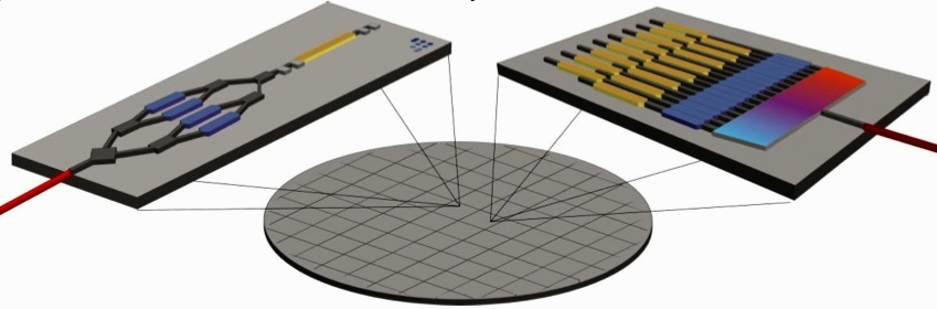
OpenLight's integrated-laser silicon photonics platform

- OpenLight is an independent silicon photonics company backed by Synopsys and Juniper Networks
- The company was created by carving out the silicon photonics arm of Juniper
- The establishment of OpenLight and its open platform highlights the growing maturity of silicon photonics as new applications emerge beyond datacom and telecom
OpenLight is coming to market with an open silicon photonics platform that includes integrated lasers and gain blocks.
Juniper has a long relationship with Synopsys, using its electronic-photonic design automation (EPDA) tools.
So when Juniper said it was spinning out its silicon photonics group, Synopsys was keen to partner. The result is OpenLight, of which Synopsys has a 75 per cent stake costing $67.5 million.
Thomas Mader, OpenLight’s chief operating officer and formerly head of Juniper’s silicon photonics unit, says OpenLight is the first company to offer an open platform that includes monolithically integrated lasers, optical amplifiers and modulators.
Juniper Networks and Synopsys
Juniper gained its silicon photonics technology in 2016 when it acquired Aurrion for $165 million.
Aurrion was a fabless silicon photonics start-up from the University of California, Santa Barbara, with a heterogeneous integration silicon photonics process that includes III-V materials, enabling integrated lasers as part of a photonic circuit.
OpenLight is now making this technology available through its partnership with the foundry Tower Semiconductor.
Juniper’s interests are mainly datacom and telecom, but it recognises the emerging opportunities for silicon photonics such as Lidar, optical computing, high-performance computing and optical interconnect.
“With this kind of technology, you want to drive volumes,” says Mader.

Juniper saw spinning out the unit and opening up access to the technology as the best way to drive volumes and reduce costs. The arrangement also benefits Juniper’s own technology needs.
Synopsys, meanwhile, believes it is the right time to back the OpenLight venture.
“We think it [the open platform] is a great opportunity for growth for Synopsys’s EPDA tools,” says John Koeter, senior vice president of marketing and strategy, solutions group at Synopsys.
OpenLight will give Synopsys insight into how the market is evolving and benefit the company’s tools and, eventually, its IP.
Business model
OpenLight is licensing its process design kit (PDK), the files that model Tower’s fabrication process. A company can enter into an agreement with Tower, access the PDK and design its silicon photonics device.
“What we are offering through Tower, and what we spent significant effort developing and showing Tower how to do, is monolithically integrating lasers and optical gain,” says Mader. “Tower is the first time we’re on a volume eight-inch [wafer] process.”
Juniper entered into a partnership with Tower Semiconductor in 2019.
“We are doing the first MPW [multi-project wafer] this summer with Tower on this process,” says Mader.
OpenLight is also providing designs it has developed and validated for several customers. “But we are not selling PICs [photonic integrated circuits]; that is not part of our plan,” says Mader.
OpenLight intends to partner with other foundries to make more widely available integrated-laser designs.

For now, though, OpenLight is focussed on ratifying its roadmap for the next two years.
“We’re going to be busy building out the component library for Tower to keep customers interested because better components make better circuits,” says Daniel Sparacin, vice president of business development and strategy at OpenLight.
OpenLight offers a 100-gigabit modulator and is working on its next-generation 200-gigabit modulator.
“We’re mostly O-band right now, and we have C-band coming up in the roadmap very shortly,” says Sparacin.
Applications
OpenLight has 400 and 800-gigabit optical designs for the data centre to help customers bring to market their PIC developments.
The company is also seeing interest from Lidar customers, particularly those pursuing coherent-based designs.
“The main reason is the integrated laser,” says Mader. “Otherwise, with standard silicon photonics, you have to attach a laser separately, which doesn’t scale well to multiple channels.” That’s because attaching multiple lasers impacts yield.
Lidar also benefits from on-chip optical amplification. “When you have a complex chip, you have a lot of losses,” says Mader.
OpenLight is working with firms pursuing optical computing for machine learning which promises greater power efficiency. “There are several of them coming to us because we can put hundreds or thousands of indium phosphide elements monolithically on a chip,” says Mader.
OpenLight says it has no position regarding co-packaged optics and whether a design uses an external light source or integrated lasers.
It believes co-packaged optics designs will eventually use integrated light sources, but its technology supports both and can even be used to make external light sources.
Overall, OpenLight says it is working with dozens of companies.
Design tools and integration
Synopsys has been an early mover with its integrated optical design automation tools. The tools include:
- OptoCompiler, a photonic IC design environment.
- The OptSim photonic circuit and system simulator.
- The Sentaurus TCAD and RSoft Photonic Device tools for process modelling and device design.
Working closely with OpenLight will benefit Synopsys’s tool environment, says Koeter. Synopsys is adding functionalities and design capabilities to its tools to support the integration of lasers. OpenLight is also providing Synopsys feedback on what will improve the experience of using its design platform.
Synopsys is one of three leading electronic design automation (EDA) tool companies. However, design tools for photonics are a more recent development.
“EDA quite a while ago is where photonic design is now going,” says Mader.
Integration is the underlying trend driving optics.
“We see the scaling already with 400- and 800-gigabit for datacom and some of the other applications; you see the shift to silicon photonics,” says Mader. “The higher the complexity, the more you see it shifting this way because there’s a cost advantage with the integrated laser and optical gain.”
Photonics may not come close to chip designs with billions of transistors. Still, photonic designs that go beyond four-channel design to ones with 32 or 64 channels or optical computing with hundreds or thousands of components are emerging.
“So you see a scaling even though it’s decades behind the electronics field,” says Mader.
With monolithically integrated lasers, yields remain high, whereas scaling a design with discrete components results in unacceptable yields.
“And so we will be able to go where you can’t go otherwise,” says Mader. “It’s not billions, but even dozens [of components] at this point is revolutionary.”

Heterogeneous integration comes of age
Silicon photonics luminaries series
Interview 7: Professor John Bowers
August has been a notable month for John Bowers.
Juniper Networks announced its intention to acquire Aurrion, the US silicon photonics start-up that Bowers co-founded with Alexander Fang. And Intel, a company Bowers worked with on a hybrid integration laser-bonding technique, unveiled its first 100-gigabit silicon photonics transceivers.
 Professor John BowersBower, a professor in the Department of Electrical and Computer Engineering at the University of California, Santa Barbara (UCSB), first started working in photonics in 1981 while at AT&T Bell Labs.
When he became interested in silicon photonics, it still lacked a good modulator and laser. "If you don't have a laser and a modulator, or a directly modulated laser, it is not a very interesting chip,” says Bowers. "So I started thinking how to do that."
Bowers contacted Mario Paniccia, who headed Intel’s silicon photonics programme at the time, and said: “What if we can integrate a laser? I think there is a good way to do it.” The resulting approach, known as heterogeneous integration, is one that both Intel and Aurrion embraced and since developed.
This is a key Bowers trait, says Aurrion co-founder, Fang: he just knows what problems to work on.
"John came up with the concept of the hybrid laser very early on," says Fang. "Recall that, at that time, silicon photonics was viewed as nothing more than people making plasma-effect phase shifters and simple passive devices. John just cut to the chase and went after combining III-V materials with silicon."
If you look at the major companies with strong photonics activities, you’ll find a leader in that group that was developed under John’s training
Fang also highlights Bowers' management skills. “John can pick players and run teams,” says Fang, who describes himself as one of those privileged to graduate out of Bowers’ research group at UCSB.
“You find yourself in an environment where John picks a team of sharp folk with complementary skills and domain expertise to solve a problem that John determines as important and has some insight on how to solve it,” says Fang. “If we look like we are going to drive off the road, he nudges with a good mix of insight, fear, and humour.”
It has resulted in some of the best trained independent thinkers and leaders in the industry, says Fang: “If you look at the major companies with strong photonics activities, you’ll find a leader in that group that was developed under John’s training”.
Silicon photonics
Bowers defines silicon photonics as photonic devices on a silicon substrate fabricated in a CMOS facility.
“Silicon photonics is not about using silicon for everything; that misses the point,” says Bowers. “The key element is using silicon as a substrate - 12-inch wafers and not 2- or 3-inch wafers - and having all the process capability a modern silicon CMOS facility brings.” These capabilities include not just wafer processing but also advanced testing and packaging.
The world is about to change and I don't think people have quite figured that out
“If you go to an advanced packaging house, they don't do 6-inch wafers and I don't know of indium phosphide and gallium arsenide wafers larger than 6 inches,” says Bowers. “The only solution is to go to silicon; that is the revolution that hasn't happened yet but it is happening now.”
Bowers adds that everything Aurrion does, there is automated test along the way. "And I think you have others; Luxtera has done a great job as well at wafer-level test and packaging," he says. "The world is about to change and I don't think people have quite figured that out."
Working with Intel was an eye-opener for Bowers, especially the process controls it applies to chip-making.
“They worry about distributions and yields, and it is clear why there are seven billion transistors on a chip and that chip will yield,” says Bowers. “When you apply that to photonics, it will take it to a whole new level.” Indeed, Bowers foresees photonics transfering to silicon.
Bowers highlights the fairly complex chips now being developed using silicon photonics.
“We have done a 2D scanner - a 32-element phased array - something one could never do in optics unless it was integrated all on one chip,” he says. The phased-array chip comprises 160 elements and is physically quite large.
This is another benefit of using 12-inch silicon wafers and fabricating the circuits in a CMOS facility. “You are not going to cost-effectively do that in indium phosphide, which I've worked on for the last 30 years,” says Bowers.
Another complex device developed at UCSB is a 2.54-terabit network-on-a-chip. “This is a larger capacity than anyone has done on any substrate,” he says.
Infinera’s latest photonic integrated circuit (PIC), for example, has a transport capacity of up to 2.4 terabit-per-second. That said, Bowers stresses that the network-on-a-chip is a research presentation while Infinera’s PIC is a commercial device.
Heterogeneous integration
Heterogeneous integration involves bonding materials such as III-V compounds onto silicon.
Bowers first worked on III-V bonding with HP to make longer wavelength - 1310nm and 1550nm - VCSELs. “We had been bonding indium phosphide and gallium arsenide to solve a fundamental problem that indium phosphide does not make good mirrors,” he says. “So I was pretty confident we could bond III-V to silicon to add gain to silicon photonics to then add all the laser capability.”
Bonding to silicon is attractive as it enables the integration of optical features that haven't been widely integrated onto any other platform, says Bowers. These include not only lasers but other active devices such as modulators and photo-detectors, as well as passive functions such as isolators and circulators.
One concern raised about heterogeneous integration and the use of III-V materials is the risk of contamination of a CMOS fabrication line.
Bowers points out that the approached used does not impact the front end of the fabrication, where silicon wafers are etched and waveguides formed. The III-V material is bonded to the wafer at the fab’s back end, the stage where metallisation occurs when making a CMOS chip.
The leading chipmakers are also experimenting with III-V materials to create faster digital devices due to their higher electron mobility. “This is part of the natural evolution of CMOS,” he says. It remains unclear if this will be adopted, but it is possible that a 5nm CMOS node will use indium phosphide.
“All the CMOS houses are doing lots of work on III-V and silicon,” says Bowers. “They have figured out how to control that contamination issue.”
New capabilities
Bowers and his team have already demonstrated the integration of new optical functions on silicon.
“Neither silicon nor indium phosphide has an isolator and one always has to use an external YIG (yttrium iron garnet) isolator to reduce the reflection sensitivity of things like widely tunable lasers,” says Bower.
His team has developed a way to bond a YIG onto silicon using the same techniques it uses for bonding III-V materials. The result is an integrated isolator device with 32dB isolation and a 2dB insertion loss, a level of performance matching those of discrete isolators.
Incorporating such functionality onto silicon creates new possibilities. “We have a paper coming out that features a 6-port circulator,” says Bowers. “It is not a tool that the community can use yet because it has never been made before but we can do that on silicon now,” he says. “That is a good new capability.”
Superior performance
Bowers stresses that heterogeneous integration can also result in optical performance superior to a III-V design alone. He cites as an example how using a silicon nitride waveguide, with its lower loss that indium phosphide or gallium arsenide, can create high-quality Q-resonators.
A Q-resonator can be viewed as a form of filter. Bowers' group have demonstrated one with a Q of 80 million. “That makes it very sensitive to a variety of things,” he says. One example is for sensors, using a Q resonator with a laser and detector to form a spectrometer.
His researchers have also integrated the Q resonator with a laser to make a widely tunable device that has a very narrow line-width: some 40kHz wide. This is a narrower than the line-width of commercially-available tunable lasers and exceeds what can be done with indium phosphide alone, he says.
Challenges
Bowers, like other silicon photonics luminaries, highlights the issues of automated packaging and automated testing, as important challenges facing silicon photonics. “Taking 10,000s of transceivers and bringing all the advanced technology - not just processing but test and packaging - that are being developed for cell phones,” he says.
Too much of photonics today is based on gold boxes and expensive transceivers. “Where Aurrion and Intel are going is getting silicon photonics to the point where photonics will be ubiquitous, cheap and high yielding,” he says. This trend is even evident with his university work. The 400-element 2.54-terabit network-on-a-chip has very high laser yields, as are its passive yields, he says.
“So, effectively, what silicon photonics can do is going up very rapidly,“ says Bowers. “If you can put it in the hands of a real CMOS player like Intel or the companies that Aurrion uses, it is going to take photonics to a whole new area that people would not have thought possible in terms of complexity.”
Yet Bowers is also pragmatic. “It still takes time,” he says. “You can demonstrate an idea, but it takes time to make it viable commercially.”
He points to the recently announced switch from Oracle that uses mid-board optics. “That is a commercial product out there now,” he says. “But is it silicon photonics? No, it is VCSEL-based; that is the battle going on now.”
VCSELs have won the initial battle in the data centre but the amount of integration the technology can support is limited. Once designers move to wavelength-division multiplexing to get to higher capacities, where planar technology is required to combine and separate the different wavelengths efficiently, that is when silicon has an advantage, he says.
The battle at 100 gigabit between VCSELs and silicon photonics is also one that Bowers believes silicon photonics will eventually win. But at 400 gigabit and one terabit, there is no way to do that using VCSELs, he says.
Status
The real win for silicon photonics is when optics moves from transceivers at the edge of the board to mid-board and eventually are integrated with a chip in the same package, he says.
Advanced chips such as switch silicon for the data centre are running into an input-output problem. There are only so many 25 gigabit-per-second signals a chip can support. Each signal, sent down a trace on a printed circuit board, typically requires equalisation circuitry at each end and that consumes power.
Most of the photonics industry has focused on telecom and datacom, and justifiably so. The next big thing will happen in the area of sensors.
A large IC packaged as a ball grid array may have as many as 5,000 bumps (balls) that are interfaced to the printed circuit board. Using photonics can boost the overall bandwidth coming on and off the chip.
“With photonics, and in particular when we integrate the laser as well as the modulator, the world doesn't see it as a photonics chip, it's an electronics chip, it just turns out that some of those bumps are optical ones and they provide much more efficient transmission of data and at much lower power,” say Bowers. A 100 terabit of even a 1000 terabit - a petabit - switch chip then becomes possible. This is not possible electrically but it is possible by integrating photonics inside the package or on the chip itself, he says.
“That is the big win eventually and that is where we help electronics extend Moore’s law,” says Bowers.
And as silicon photonics matures, other applications will emerge - More than Moore’s law - like the use of photonics for sensors.
“Most of the photonics industry has focused on telecom and datacom, and justifiably so,” says Bowers. “The next big thing will happen in the area of sensors.”
Professor Bowers was interviewed before the Juniper Networks announcement
Intel's 100-gigabit silicon photonics move
Intel has unveiled two 100-gigabit optical modules for the data centre made using silicon photonics technology.
 Alexis Bjorlin
The PSM4 and CWDM4/CLR4 100-gigabit modules mark the first commercial application of a hybrid integration technique for silicon photonics, dubbed heterogeneous integration, that Intel has been developing for years.
Intel's 100-gigabit module announcement follows the news that Juniper Networks has entered into an agreement to acquire start-up, Aurrion, for $165 million. Aurrion is another silicon photonics player developing this hybrid integration technology for its products.
Hybrid integration
With heterogeneous integration, materials such as indium phosphide and gallium arsenide can be bonded to the silicon substrate before the 300mm wafer is processed to produce the optical circuit. Not only can lasers be added to silicon but other active devices such as modulators and photo-detectors as well as passive functions such as isolators and circulators.
There is no alignment needed; we align the laser with lithography
Intel is using the technique to integrate the laser as part of the 100-gigabit transceiver designs.
"Once we apply the light-emitting material down to the silicon base wafer, we define the laser in silicon," says Alexis Bjorlin, vice president and general manager, Intel Connectivity Group. “There is no alignment needed; we align the laser with lithography.”
Intel claims it gets the highest coupling efficiency between the laser and the optical waveguide and modulator because it is lithographically defined and requires no further alignment.
100-gigabit modules
Intel is already delivering the 100-gigabit PSM4 module. “First volume shipments are happening now,” says Bjorlin. Microsoft is one Internet content provider that is using Intel’s PSM4.
The chip company is also sampling a 100-gigabit CWDM4 module that also meets the more demanding CLR4 Alliance’s optical specification. The 100-gigabit CLR4 module can be used without forward-error correction hardware and is favoured for applications where latency is an issue such as high-performance computing.
Intel is not the first vendor to offer PSM4 modules, nor is it the first to use silicon photonics for such modules. Luxtera and Lumentum are shipping silicon photonics-based PSM4 modules, while STMicroelectronics is already supplying its PSM4 optical engine chip.
We are right on the cusp of the real 100-gigabit connectivity deployments
“Other vendors have been shipping PSM4 modules for years, including large quantities at 40 gigabit,” says Dale Murray, principal analyst at LightCounting Market Research. “Luxtera has the clear lead in silicon photonics-based PSM4 modules but a number of others are shipping them based on conventional optics.”
The PSM4 is implemented using four independent 25-gigabit channels sent over a single-mode ribbon fibre. Four fibres are used for transmission and four fibres for receive.
“The PSM4 configuration is an interesting design that allows one laser to be shared among four separate output fibres,” says Murray. “As Luxtera has shown, it is an effective and efficient way to make use of silicon photonics technology.”
The CWDM4 is also a 4x25-gigabit design but uses wavelength-division multiplexing and hence a single-mode fibre pair. The CWDM4 is a more complex design in that an optical multiplexer and demultiplexer are required and the four lasers operate at different wavelengths.
“While the PSM4 module does not break new ground, Intel’s implementation of WDM via silicon photonics in a CWDM4/CLR4 module could be more interesting in a low-cost QSFP28 module,” says Murray. WDM-based QSFP28 modules are shipping from a number of suppliers that are using conventional optics, he says.
Intel is yet to detail when it will start shipping the CWDM4/CLR4 module.
Market demand
Bjorlin says the PSM4 and the CWDM4/CLR4 will play a role in the data centre. There are applications where being able to break out 100-gigabit into 25-gigabit signals as offered by the PSM4 is useful, while other data centre operators prefer a duplex design due to the efficient use of fibre.
“We are right on the cusp of the real 100-gigabit connectivity deployments,” she says.
As for demand, Bjorlin expects equal demand for the two module types in the early phases: “Longer term, we will probably see more demand for the duplex solution”.
LightCounting says that 100-gigabit PSM4 modules took an early lead in the rollout of 100 Gigabit Ethernet, with VCSEL-based modules not far behind.
“Some are shipping CWDM4/CLR4 and we expect that market to ramp,” says Murray. “Microsoft and Amazon Web Services seem to like PSM4 modules while others want to stick with modules that can use duplex fibre.
 Source: Intel
Data centre switching
“One of the most compelling reasons to drive silicon photonics in the future is that it is an integratable platform,” says Bjorlin.
Switch silicon from the likes of Broadcom support 3.2 terabits of capacity but this will increase to 6.4 terabits by next year and 12.8 terabits using 4-level pulse amplitude modulation (PAM-4) signalling by 2018 (see chart). And by 2020, 25.6-terabit capacity switch chips are expected.
The demand for 100 gigabit is for pluggable modules that fit into the front panels of data center switches. But the market is evolving to 400-gigabit embedded optics that sit on the line card, she says, to enable these emerging higher-capacity switches. Intel is a member of the Consortium of On-Board Optics (COBO) initiative that is being led by Microsoft.
“When you get to 25.6-terabit switches, you start to have a real problem getting the electrical signals in and out of the switch chip,” says Bjorlin. This is where silicon photonics can play a role in the future by co-packaging the optics alongside the switch silicon.
“There will be a need for an integrated solution that affords the best power consumption, the best bandwidth-density that we can get and effectively position silicon photonics for optical I/O [input/output],” says Bjorlin. “Ultimately, that co-packaging is inevitable.”
Juniper Networks to acquire Aurrion for $165 million
The announcement of the acquisition was low key. A CTO blog post and a statement that Juniper Networks had entered into an agreement to acquire Aurrion, the fabless silicon photonics start-up. No fee was mentioned.
However, in the company's US Securities and Exchange Commission filing, Juniper values the deal at approximately $165 million. "The Company believes the acquisition will help to fuel its long-term competitive advantage by enabling cost-effective, high-density, high-speed optical networks," it said. The deal is expected to be closed this quarter.

But the deal is significant for a number of reasons.
First, Aurrion, like Intel, is a proponent of heterogeneous integration, combining indium phosphide and other technologies on a silicon wafer platform through bonding. The approach has still to be proven in commercial volumes but it promises the use of III-V materials on 12-inch silicon wafers manufactured in a chip fabrication plant.
Aurrion has made tunable lasers for telecom that cover both the C- and L-bands, as well as uncooled laser arrays for datacom applications. The start-up has also been developing high-speed transceivers for the data centre.
The company has also been working on the manufacturing aspects of silicon photonics, a considerable undertaking. These include automated wafer-scale testing, connecting fibre to a silicon photonics chip, and packaging.
Juniper is thus getting an advanced silicon photonics technology suited for volume manufacturing that it will use to advance its data centre networking offerings.
Juniper may choose to make its own optical transceivers but, more likely, it will use silicon photonics as part of its switch designs to tackle issues of data centre scaling and the continual challenge of growing power consumption. It could also use the technology for its IP core routers and longer term, to tackle I/O issues alongside custom ASICs.
Systems vendors drive silicon photonics
The Aurrion acquisition also highlights how it is systems vendors that are acquiring silicon photonics start-ups rather than the traditional optical component and module makers.
This is partly a recognition that silicon photonics' main promise is as a systems technology. Acacia, the coherent transmission specialist, is one company that has shown how silicon photonics can benefit optical module design but the technology's longer-term promise is for systems design rather than optical modules.
A consequence of such acquisitions by systems vendors is that technology being developed by silicon-photonics start-ups is being swallowed within systems houses for their own use and not for the merchant market. Systems vendors have deep pockets to develop the technology but it will be for their own use. For the wider community, silicon photonics technology being developed by the likes of Aurrion is no longer available.
This is what AIM Photonics, the US public-private partnership that is developing technology for integrated photonics, is looking to address: to advance the manufacturing of silicon photonics, making the resulting technology available to small to medium sized businesses and entrepreneurial ventures. However, AIM Photonics is one year into a five-year venture.
Implications
Should major systems vendors owning silicon photonics technology in-house concern the traditional optical component vendors?
Not for now.
Optical transceiver sales continue to grow and the bulk of designs are not integrated. And while silicon photonics is starting to be used for integrated designs, it is competing against the established technologies of indium phosphide and gallium arsenide.
But as photonics moves closer to the silicon and away from a system's faceplate, silicon photonics becomes more strategically important and this is where systems vendors can start developing custom designs.
Must the systems houses own the technology to do that?
Not necessarily, but they will need silicon photonics design expertise, and in the case of Juniper, it can hit the ground running with Aurrion.
Longer term, it will be the much larger chip industry that will drive silicon photonics rather than the optical industry. There are chip foundries now that are making silicon photonic ICs as there are top-ten chip companies such as Intel and STMicroelectronics. But ultimately it will be a very different supply chain that will take shape.
It is early days but Juniper's acquisition is the latest indicator that it is the systems vendors that are moving first at the very beginnings of this new ecosystem.
Aurrion mixes datacom and telecom lasers on a wafer
 "There is an inevitability of the co-mingling of electronics and optics and we are just at the beginning"
Eric Hall, Aurrion
Aurrion's long-term vision for its heterogeneous integration approach to silicon photonics is to tackle all stages of a communication link: the high-bandwidth transmitter, switch and receiver. Heterogeneous integration refers to the introduction of III-V material - used for lasers, modulators and receivers - onto the silicon wafer where it is processed alongside the silicon using masks and lithography.
In a post-deadline paper given at OFC/NFOEC 2013, the fabless start-up detailed the making of various transmitters on a silicon wafer. These include tunable lasers for telecom that cover the C- and L-bands, and uncooled laser arrays for datacom.
The lasers are narrow-linewidth tunable devices for long-haul coherent applications. According to Aurrion, achieving a narrow-linewidth laser typically requires an external cavity whose size makes it difficult to produce a compact design when integrated with the modulator.
Having a tunable laser integrated with the modulator on the same silicon photonics platform will enable compact 100 Gigabit coherent pluggable modules. "The 100 Gig equivalent of the tunable XFP or SFP+," says Eric Hall, vice president of business development at Aurrion.
Hall admits that traditional indium-phosphide laser manufacturers will likely integrate tunable lasers with the modulator to produce compact narrow-linewidth designs. "There will be other approaches but it is exciting that we can now make this laser and modulator on this platform," says Hall. "And it becomes very exciting when you make these on the same wafer as high-volume datacom components."
 Aurrion's vision of a coherent transmitter and a 16-laser array made on the same wafer. Source: Aurrion
The wafer's datacom devices include a 4-channel laser array for 100GBASE-LR4 10km reach applications and a 400 Gigabit transmitter design comprising 2x8 wavelength division multiplexing (WDM) arrays for a 16x25Gbps design, each laser spaced 200GHz apart. These could be for 10km or 40km applications depending on the modulator used. "These arrays are for uncooled applications," says Hall. "The idea is these don't have to be coarse WDM but tighter-spaced WDM that hold their wavelength across 20-80oC."
Coarse WDM-based laser arrays do not require a thermo-electric cooler (TEC) but the larger spacing of the wavelengths makes it harder to design beyond 100 Gigabit, says Hall: "Being able to pack in a bunch of wavelengths yet not need a TEC opens up a lot of applications."
Such lasers coupled with different modulators could also benefit 100 Gigabit shorter-reach interfaces currently being discussed in the IEEE, including the possibility of multi-level modulation schemes, says the company.
Aurrion says it is seeing the trend of photonics moving closer to the electronics due to emerging applications.
"Electronics never really noticed photonics because it was so far away and suddenly photonics has encroached into its personal space," says Hall. "There is an inevitability of the co-mingling of electronics and optics and we are just at the beginning."