
Juniper Networks to acquire Aurrion for $165 million
The announcement of the acquisition was low key. A CTO blog post and a statement that Juniper Networks had entered into an agreement to acquire Aurrion, the fabless silicon photonics start-up. No fee was mentioned.
However, in the company's US Securities and Exchange Commission filing, Juniper values the deal at approximately $165 million. "The Company believes the acquisition will help to fuel its long-term competitive advantage by enabling cost-effective, high-density, high-speed optical networks," it said. The deal is expected to be closed this quarter.

But the deal is significant for a number of reasons.
First, Aurrion, like Intel, is a proponent of heterogeneous integration, combining indium phosphide and other technologies on a silicon wafer platform through bonding. The approach has still to be proven in commercial volumes but it promises the use of III-V materials on 12-inch silicon wafers manufactured in a chip fabrication plant.
Aurrion has made tunable lasers for telecom that cover both the C- and L-bands, as well as uncooled laser arrays for datacom applications. The start-up has also been developing high-speed transceivers for the data centre.
The company has also been working on the manufacturing aspects of silicon photonics, a considerable undertaking. These include automated wafer-scale testing, connecting fibre to a silicon photonics chip, and packaging.
Juniper is thus getting an advanced silicon photonics technology suited for volume manufacturing that it will use to advance its data centre networking offerings.
Juniper may choose to make its own optical transceivers but, more likely, it will use silicon photonics as part of its switch designs to tackle issues of data centre scaling and the continual challenge of growing power consumption. It could also use the technology for its IP core routers and longer term, to tackle I/O issues alongside custom ASICs.
Systems vendors drive silicon photonics
The Aurrion acquisition also highlights how it is systems vendors that are acquiring silicon photonics start-ups rather than the traditional optical component and module makers.
This is partly a recognition that silicon photonics' main promise is as a systems technology. Acacia, the coherent transmission specialist, is one company that has shown how silicon photonics can benefit optical module design but the technology's longer-term promise is for systems design rather than optical modules.
A consequence of such acquisitions by systems vendors is that technology being developed by silicon-photonics start-ups is being swallowed within systems houses for their own use and not for the merchant market. Systems vendors have deep pockets to develop the technology but it will be for their own use. For the wider community, silicon photonics technology being developed by the likes of Aurrion is no longer available.
This is what AIM Photonics, the US public-private partnership that is developing technology for integrated photonics, is looking to address: to advance the manufacturing of silicon photonics, making the resulting technology available to small to medium sized businesses and entrepreneurial ventures. However, AIM Photonics is one year into a five-year venture.
Implications
Should major systems vendors owning silicon photonics technology in-house concern the traditional optical component vendors?
Not for now.
Optical transceiver sales continue to grow and the bulk of designs are not integrated. And while silicon photonics is starting to be used for integrated designs, it is competing against the established technologies of indium phosphide and gallium arsenide.
But as photonics moves closer to the silicon and away from a system's faceplate, silicon photonics becomes more strategically important and this is where systems vendors can start developing custom designs.
Must the systems houses own the technology to do that?
Not necessarily, but they will need silicon photonics design expertise, and in the case of Juniper, it can hit the ground running with Aurrion.
Longer term, it will be the much larger chip industry that will drive silicon photonics rather than the optical industry. There are chip foundries now that are making silicon photonic ICs as there are top-ten chip companies such as Intel and STMicroelectronics. But ultimately it will be a very different supply chain that will take shape.
It is early days but Juniper's acquisition is the latest indicator that it is the systems vendors that are moving first at the very beginnings of this new ecosystem.
Cortina unveils multi-channel dispersion compensation chip
Cortina Systems has announced its latest electronic dispersion compensation (EDC) chip. The CS4342 is a compact device that supports eight duplex 10 Gigabit-per-second (Gbps) links.
"Some customers are doing 2,000 signals at 10 Gig across the backplane"
Scott Feller, Cortina
The chip is suited for use with optical modules and on line cards to counter the effect of transmission distortion where a bit's energy leaks into one or more adjacent bits, known as inter-symbol interference (ISI).
The Cortina device can be used for 10, 40 and 100Gbps line card and backplane designs and supports copper cable and optical fibre standards such as the multimode 10GBASE‐LRM and the 80km 10GBASE‐ZR interface.
Significance
Routeing high-speed signals from an ASIC to the various high-speed interfaces - 10Gbps and greater - is becoming harder as more interfaces are crammed onto a card.
"Boards are getting denser: from 48 ports to 96," says Scott Feller, director of the EDC product line at Cortina Systems. The issue with an ASIC on the board is that the distance it can span to the modules is only about 6-8 inches (~15-20cm). Placing the PHY chip on the board relaxes this constraint.
 The use of the octal EDC chip between a line card IC and SFP+ optical transceivers. Source: Cortina Systems
Vendors also gain greater flexibility in terms of the interfaces they can support. "These types of PHYs allow them [designers] to avoid having to make hard decisions," says Feller. "They put the PHY in front of the optical connector and they almost get every single optical format on the market."
The platforms using such EDC PHYs include data centre switches and telecom platforms such as packet optical transport systems (P-OTS). Data centre switches typically support Direct Attach Copper cable - a market area that has been growing significantly, says Cortina - and short-reach optical interfaces. For P-OTS the interfaces include the 10GBASE-ZR where EDC is a necessity.
The device is also being used for system backplanes where bandwidth requirements are increasing significantly. "Some customers are doing 2,000 signals at 10 Gig across the backplane," says Feller. "Now that there are so many signals - so much crosstalk - and the ASICs are further away from the backplane, so PHYs are starting to be put into systems."
 EDC employed in a backplane design. Source: Cortina Systems
Chip details
Cortina claims the 17x17 ball grid array CS4342 is a third smaller than competing devices. The chip compensates the received signal in the analogue domain. An on-chip DSP calculates the filter's weights to counter ISI while the filtering is performed using analogue circuitry. As a result, the EDC has a latency of 1ns only.
Cortina has dual, quad and now octal EDC ICs. It says that the delay between the different devices is the same such that both an octal and dual chip can be used to implement a 10-channel 100 Gig interface, for example the 10x10 MSA. In turn, future line cards supporting four 100Gbps interfaces would use five octal PHYs ICs.
The CS4342 is available in sample form and will enter production from October.
What next
"This type of product is at the very end of the food chain so there is always macro developments that could change the market," says Feller. Silicon photonics is one but Feller expects that it will be years before the technology is adopted widely in systems.
The external EDC PHYs must also compete with PHYs integrated within custom ASIC designs and FPGAs. "We always have to be ahead of the cost and performance curves on the PHY," says Feller. "If not, they [companies] are just going to integrate PHYs into their ASICs and FPGAs."
Meanwhile, Cortina says it has two more EDC devices in development.
Rational and innovative times: JDSU's CTO Q&A Part II
"What happens after 100 Gig is going to be very interesting"
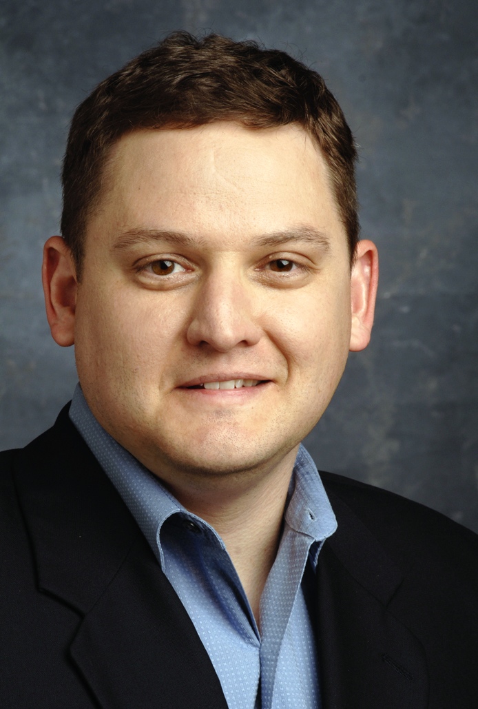
Brandon Collings (right), JDSU
How has JDS Uniphase (JDSU) adapted its R&D following the changes in the optical component industry over the last decade?
JDSU has been a public company for both periods [the optical boom of 1999-2000 and now]. The challenge JDSU faced in those times, when there was a lot of venture capital (VC) money flowing into the system, was that the money was sort of free money for these companies. It created an imbalance in that the money was not tied to revenue which was a challenge for companies like JDSU that ties R&D spend to revenue. You also have much more flexibility [as a start-up] in setting different price points if you are operating on VC terms.
The situation now is very straightforward, rational and predictable.
There is not a huge army of R&D going on. That lack of R&D does not speed up the industry but what it does do is allow those companies doing R&D - and there is still a significant number - a lot of focus and clarity. It also requires a lot of partnership between us, our customers [equipment makers] and operators. The people above us can't just sit back and pick and choose what they like today from myriad start-ups doing all sorts of crazy things.
We very much appreciate this rational time. Visions can be more easily discussed, things are more predictable and everyone is playing from a similar set of rules.
Given the changes at the research labs of system vendor and operators, is there a risk that insufficient R&D is being done, impeding optical networking's progress?
It is hard to say absolutely not as less people doing things can slow things down. But the work those labs did, covered a wide space including outside of telecom.
There is still a sufficient critical mass of research at placed like Alcatel-Lucent Bell Labs, AT&T and BT; there is increasingly work going on in new regions like Asia Pacific, and a lot more in and across Europe. It is also much more focussed - the volume of workers may have decreased but the task still remains in hand.
"There are now design tradeoffs [at speeds higher than 100Gbps] whereas before we went faster for the same distance"
How does JDSU foster innovation and ensure it is focussing on the right areas?
I can't say that we have at JDSU a process that ensures innovation. Innovation is fleeting and mysterious.
We stay very connected to our key customers who are more on the cutting edge. We have very good personal and professional relationships with their key people. We have the same type of relationship with the operators.
I and my team very regularly canvass and have open discussions about what is coming. What does JDSU see? What do you see? What technologies are blossoming? We talk through those sort of things.
That isn't where innovation comes from. But what that can do is sow the seeds for the opportunity for innovation to happen.
We take that information and cycle it through all our technology teams. The guys in the trenches - the material scientists, the free-space optics design guys - we try to educate them with as much of an understanding of the higher-level problems that ultimately their products, or the products they design into, will address.
What we find is that these guys are pretty smart. If you arm them with a wider understanding, you get a much more succinct and powerful innovation than if you try to dictate to a material scientist here is what we need, come back when you are done.
It is a loose approach, there isn't a process, but we have found that the more we educate our keys [key guys] to the wider set of problems and the wider scope of their product segments, the more they understand and the more they can connect their sphere of influence from a technology point of view to a new capability. We grab that and run with it when it makes sense.
It is all about communicating with our customers and understanding the environment and the problem, then spreading that as wide as we can so that the opportunity for innovation is always there. We then nurse it back into our customers.
Turning to technology, you recently announced the integration of a tunable laser into an SFP+, a product you expect to ship in a year. What platforms will want a tunable laser in this smallest pluggable form factor?
The XFP has been on routers and OTN (Optical Transport Network) boxes - anything that has 10 Gig - and those interfaces have been migrated over to SFP+ for compactness and face plate space. There are already packet and OTN devices that use SFP+, and DWDM formats of the SFP+, to do backhaul and metro ring application. The expectation is that while there are more XFP ports today, the next round of equipment will move to SFP+.
Certainly the Ciscos, Junipers and the packet guys are using tunable XFPs in great volume for IP over DWDM and access networks, but the more telecom-centric players riding OTN links or maybe native Ethernet links over their metro rings are probably the larger volume.
What distance can the tunable SFP+ achieve?
The distances will be pretty much the same as the tunable XFP. We produce that in a number of flavours, whether it is metro and long-haul. The initial SFP+ will like be the metro reaches, 80km and things like that.
What is the upper limit of the tunable XFP?
We produce a negative chirp version which can do 80km of uncompensated dispersion, and then we produce a zero chirp which is more indicative of long-haul devices.
In that case the upper limit is more defined by the link engineering and the optical signal-to-noise ratio (OSNR), the extent of the dispersion compensation accuracy and the fibre type. It starts to look and smell like a long-haul lithium niobate transceiver where the distances are limited by link design as much as by the transceiver itself. As for the upper limit, you can push 1000km.
An XFP module can accommodate 3.5W while an SFP+ is about 1.5W. How have you reduced the power to fit the design into an SFP+?
It may be a generation before we get to that MSA level so we are working with our customers to see what level they can tolerate. We'll have to hit a lot less that 3.5W but it is not clear that we have to hit the SFP+ MSA specification. We are already closer now to 1.5W than 3.5W.
"I can't say that we have at JDSU a process that ensures innovation. Innovation is fleeting and mysterious."
Semiconductors now play a key role in high-speed optical transmission. Will semiconductors take over more roles and become a bigger part of what you do?
Coherent transmission [that uses an ASIC incorporating a digital signal processor (DSP)] is not going away. There is a lot of differentiation at the moment in what happens in that DSP, but I think overall it is going to be a tool the system houses use to get the job done.
If you look at 10 Gig, the big advancement there was FEC [forward error correction] and advanced FEC. In 2003 the situation was a lot like it is today: who has the best FEC was something that was touted.
If you look at coherent technology, it is certainly a different animal but it is a similar situation: that is, the big enabler for 40 and 100 Gig. Coherent is advanced technology, enhanced FEC was advanced technology back then, and over time it turned into a standardised, commoditised piece that is central and ubiquitously used for network links.
Coherent has more diversity in what it can do but you'll see some convergence and commoditisation of the technology. It is not going to replace or overtake the importance of photonics. In my mind they play together intimately; you can't replace the functions of photonics with electronics any time soon.
From a JDSU perspective, we have a lot of work to do because the bulk of the cost, the power and the size is still in the photonics components. The ASIC will come down in power, it will follow Moore's Law, but we will still need to work on all that photonics stuff because it is a significant portion of the power consumption and it is still the highest portion of the cost.
JDSU has made acquisitions in the area of parallel optics. Given there is now more industry activity here, why isn't JDSU more involved in this area?
We have been intermittently active in the parallel optics market.
The reality is that it is a fairly fragmented market: there are a lot of applications, each one with its own requirements and customer base. It is tough to spread one platform product around these applications. That said, parallel optics is now a mainstay for 40 and 100 Gig client [interfaces] and we are extremely active in that area: the 4x10, 4x25 and 12x10G [interfaces]. So that other parallel optics capability is finding its way into the telecom transceivers.
We do stay active in the interconnect space but we are more selective in what we get engaged in. Some of the rules there are very different: the critical characteristics for chip interconnect are very different to transceivers, for example. It may be much better to have on-chip optics versus off-chip optics. Obviously that drives completely different technologies so it is a much more cloudy, fragmented space at the moment.
We are very tied into it and are looking for those proper opportunities where we do have the technologies to fit into the application.
How does JDSU view the issues of 200, 400 Gigs and 1 Terabit optical transmission?
What happens after 100 Gig is going to be very interesting.
Several things have happened. We have used up the 50GHz [DWDM] channel, we can't go faster in the 50GHz channel - that is the first barrier we are bumping into.
Second, we're finding there is a challenge to do electronics well beyond 40 Gigabit. You start to get into electronics that have to operate at much higher rates - analogue-to-digital converters, modulator drivers - you get into a whole different class of devices.
Third, we have used all of our tools: we have used FEC, we are using soft-decision FEC and coherent detection. We are bumping into the OSNR problem and we don't have any more tools to run lines rates that have less power to noise yet somehow recover that with some magic technology like FEC at 10 Gig, and soft decision FEC and coherent at 40 and 100 Gig.
This is driving us into a new space where we have to do multi-carrier and bigger channels. It is opening up a lot of flexibility because, well, how wide is that channel? How many carriers do you use? What type of modulation format do you use?
What format you use may dictate the distance you go and inversely the width of the channel. We have all these new knobs to play with and they are all tradeoffs: distance versus spectral efficiency in the C-band. The number of carriers will drive potentially the cost because you have to build parallel devices. There are now design tradeoffs whereas before we went faster for the same distance.
We will be seeing a lot of devices and approaches from us and our customers that provide those tradeoffs flexibly so the carriers can do the best they can with what mother nature will allow at this point.
That means transponders that do four carriers: two of them do 200 Gig nicely packed together but they only achieve a few hundred kilometers, but a couple of other carriers right next door go a lot further but they are a little bit wider so that density versus reach tradeoff is in play. That is what is going to be necessary to get the best of what we can do with the technology.
That is the transmission side, the transport side - the ROADMS and amplifiers - they have to accommodate this quirky new formats and reach requirements.
We need to get amplifiers to get the noise down. So this is introducing new concepts like Raman and flex[ible] spectrum to get the best we can do with these really challenging requirements like trying to get the most reach with the greatest spectral efficiency.
How do you keep abreast of all these subject areas besides conversations with customers?
It is a challenge, there aren't many companies in this space that are broader than JDSU's optical comms portfolio.
We do have a team and the team has its area of focus, whether it is ROADMs, modulators, transmission gear or optical amplifiers. We segment it that way but it is a loose segmentation so we don't lose ideas crossing boundaries. We try to deal with the breadth that way.
Beyond that, it is about staying connected with the right people at the customer level, having personal relationships so that you can have open discussions.
And then it is knowing your own organisation, knowing who to pull into a nebulous situation that can engage the customer, think on their feet and whiteboard there and then rather than [bringing in] intelligent people that tend to require more of a recipe to do what they are doing.
It is all about how to get the most from each team member and creating those situations where the right things can happen.
For Part I of the Q&A, click here