
EZchip packs 100 ARM cores into one networking chip
 The Tile-Mx100. Source: EZchip
- The industry's first detailed chip featuring 100, 64-bit ARM cores
- The Tile-Mx devices will perform control plane processing and data plane processing
- The 100-core chip will have 100 Gigabit Ethernet ports and support 200 Gigabit duplex traffic
EZchip has detailed the industry's first 100-core processor. Dubbed the Tile-Mx100, the processor will be the most powerful of a family of devices aimed at such applications as software-defined networking (SDN), network function virtualisation (NFV), load-balancing and security. Other uses include video processing and application recognition, to identify applications riding over a carrier's network.
Known for its network processors, EZchip has branched out to also include general-purpose processors following its acquisition of multicore specialist, Tilera. It now competes with such companies as Broadcom, Cavium and Intel.
What's new about the EZchip Tile-Mx100 is that it is the first such processor with 100 cache-coherent programmable CPU cores and it is by far the largest 64-bit ARM processor yet announced
EZchip's NPS network processor is a custom IC designed to maximise packet-processing performance. The Tile-Mx also targets networking but using standard ARM cores. Engineers will benefit from open source software, third-party applications and ARM development tools. "We believe the market needs a standard, open architecture," says Amir Eyal, vice president of business development at EZchip.
"A multicore standard processor tailored for networking is nothing new; numerous such processors have been available for years from several vendors," says Tom Halfhill, senior analyst at The Linley Group. "What's new about the EZchip Tile-Mx100 is that it is the first such processor with 100 cache-coherent programmable CPU cores and it is by far the largest 64-bit ARM processor yet announced."
EZchip has detail three Tile-Mx devices, the most powerful being the Tile-Mx100 that uses 100, 64-bit ARM Cortex-A53 cores. The Cortex-A53 is newer and smaller than the Cortex-A57, and has a relatively low power consumption. Handset and tablet designs are also using the ARM Cortex-A53 core. Both the A53 and A57 cores use the ARMv8-A instruction set.
"We have taken the A53 in order to put more cores on the die," says Eyal. "The idea with networking applications is that the more packets you can process in parallel, the better." A chip hosting many, smaller cores helps meet this goal.
Tile-Mx architecture
The Tile-Mx100 device will process traffic at rates up to 200 Gigabit-per-second (Gbps) rates, or 200 Gbps duplex. In contrast, EZchip's NPS family of devices has a roadmap with a traffic processing performance of 400 Gbps to 800 Gbps duplex.
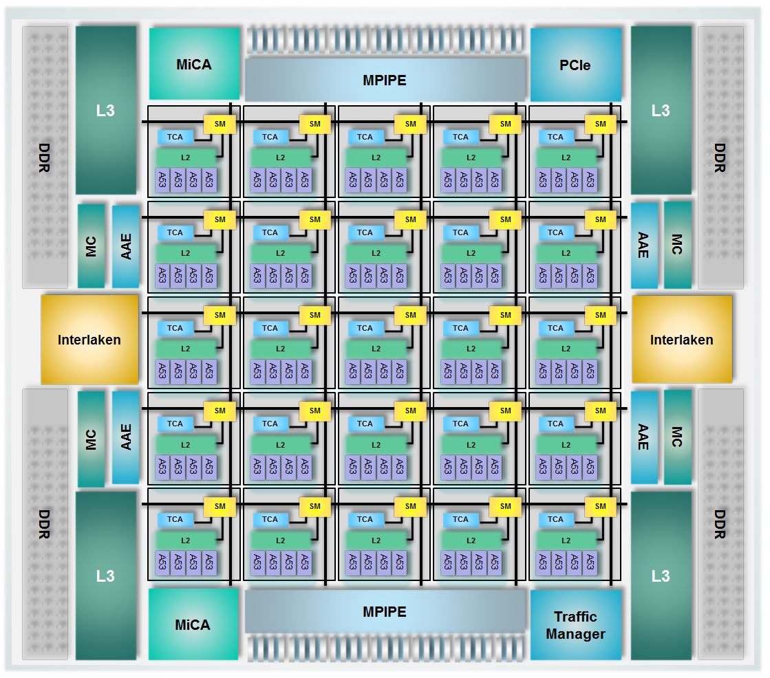
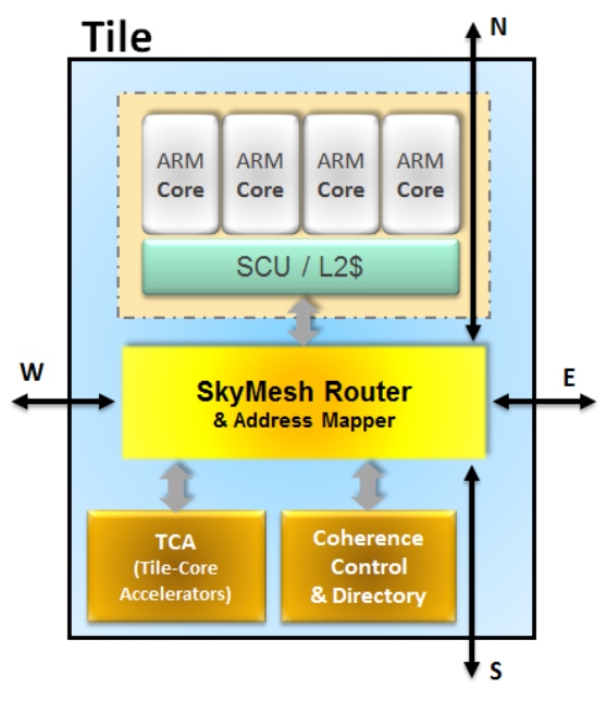
The Tile-Mx uses a two-level architecture. The 100 cores are partitioned into 25 processing clusters or tiles, each comprising four ARM cores that share network acceleration hardware and level-2 cache memory. Each tile also features router hardware, part of the chip's interconnect network that handles the tile's input/ output (I/O) requirements.
 Source: EZchip
"The key technology for the Tile-Mx architecture is the interconnect that enables 100 CPUs to be connected in a coherent manner," says Jag Bolaria, principal analyst at The Linley Group.
"There are five different networks [part of the mesh] that interconnect the 100 cores in parallel, preventing bottlenecks and contention," says Eyal. The mesh also ensures that each core can talk to the chip's I/O and to the memory. The mesh is a fifth iteration, having been improved with each generation of chip design, says Eyal, and has a total bandwidth of 25 Terabits.
The mesh also implements cache coherency, an important aspect of multi-processor design that ensures that cache memory is updated when accessed by any of the cores without needing to introduce idle states first.
Other chip features include a traffic manager, essentially the one used for EZchip's NPUs, which prioritises traffic, allocates bandwidth and prevents packet loss. There are also hardware units (see MiCA blocks in main chip diagram), developed by Tilera, which do preliminary packet classification before presenting the packets to the cores.
The chip's I/O includes 1, 10, 25, 40, 50 and 100 Gigabit Ethernet interfaces, the Interlaken interface and PCI Express, used to connect the chip to a host processor such as an Intel x86 microprocessor.
The idea with networking applications is that the more packets you can process in parallel, the better
EZchip is not detailing the device's interface mix or such metrics as the chip's pin-count, clock speed or power consumption. However, EZchip says the chip's power consumption will be under 100W.
When a packet is presented to the chip, it is assigned to a core which processes it to completion before sending it typically to the I/O. For the programmer, the 100-core device appears as a single processor; it is the hardware on-chip that handles the details, sending an incoming packet to the next free core.
Ezchip shows examples of possible platforms that could use the Tile-Mx.
One is a 1-rack-unit-high pizza box in the data centre used to deliver virtual network functions. Such a NFV server would benefit from the Tile-Mx's hardware-accelerated table look-ups, packet classification and packet flow management in and out of the device. Another design example is using the device for an intelligent network interface card (NIC) in a standard Intel x86-based server.
The two other Tile-Mx family devices will use 36 and 64 Cortex-A53 cores. First Tile-Mx samples are expected in the second half of 2016.
Multicore trends
The Linley Group says that despite the unprecedented 100 ARM cores, EZchip's family of device faces competition. Moreover, the trend to increase core-count has its limits.
EZchip is already shipping a 72-core processor it acquired from Tilera although the device is not ARM-based. And Cavium's largest processor has 48 cores, says Halfhill. Broadcom's largest processor has only 20 cores, but those CPUs are quad-threaded, so the processor can handle up to 80 packet streams. "Not quite as many as the Tile-Mx100, but it is in the same ballpark," says Halfhill.
"Keep in mind that Tile-Mx100 production is about two years out; a lot can happen in two years," adds Halfhill.
According to Bolaria, multicore designs are good for applications that are highly parallelised such as packet processing and deep packet processing. But NPUs are better if all that is being done is packet processing.
"Many cores is not particularly good for applications that need good single-thread performance," says Bolaria. "This is where [an Intel] Xeon will shine — for applications such as high-performance computing, simulations and algorithms."
Coherent interconnects also limit CPU scaling, says Bolaria. Tile-Mx gets around the interconnect limitation by clustering four ARM cores into a tile, so that effectively 25 nodes only are connected. "With more nodes, it becomes difficult to maintain cache coherency and performance," says Bolaria.
Another limitation is partitioning applications into smaller chunks for execution on 100 cores. Some tasks are serial by nature and cannot benefit from parallel processing. "Amdahl’s law limits performance gains from adding more CPUs," says Bolaria.
EZchip expands the role of the network processor
- EZchip's NPS-400 will be a 200Gbps duplex chip capable of layer 2 to layer 7 network processing
- The device is being aimed at edge routers and the data centre
- First samples by year end
EZchip Semiconductor has announced a class of network processor capable of performing traditional data plane processing as well as higher layer networking tasks. EZchip's announced NPS will extend the role of the network processor to encompass layer two to layer seven of the network. Source: EZchip
"It [the device family] is designed to provide processing for all the networking layers, from layer two all the way to layer seven," says Amir Eyal, EZchip’s vice president of business development. Network processors typically offer layer-two and layer-three processing only.
The device family, called the network processor for smart networks (NPS), is being aimed at Carrier Ethernet edge router platforms, the traditional telecom application for network processors.
But the NPS opens up new opportunities for EZchip in the data centre, such as security, load balancing and software-defined networking (SDN). Indeed EZchip says the NPS market will double the total addressable market to US$2.4bn by 2016.
"SDN is supposedly a big deal in the data centre," says Eyal. Because SDN separates the control plane from the data plane, it implies that the data plane becomes relatively simple. In practice the opposite is true: the data processing becomes more complex requiring the recognition and handling of packets having different encapsulation schemes, says Eyal.
The NPS borrows architectural elements of EZchip's existing high-end NPUs but the company has added an ARC 32-bit reduced instruction set computer (RISC) processor which it has redesigned to create the basic packet-processing computing node: the CTOP (C-programmable task-optimised processor).
EZchip has announced two NPS devices: The NPS-200 and the more processing-capable NPS-400. The NPS-400 is a 200 Gigabit-per-second (Gbps) duplex chip with 256 CTOPs, giving it twice the packet-processing performance of EZchip's latest NP-5 NPU. The NPS-400 will also have 800 Gigabit of input/ output. The NPS-200 design will have 128 CTOPs.
As a result of adding the ARC, the NPS family will be C-programmable whereas NPUs are programmed using assembly language or micro-code. The CTOP will also be able to processes 16 instruction threads whereas the standard ARC is single thread.
The NPS also features an on-chip traffic manager which controls the scheduling of traffic after it has been processed and classified.
The power consumption of the NPS has yet to be detailed but Eyal says it will be of the order of the NP-5 which is 60W.
EZchip says up to eight NPS chips could be put on a line card, to achieve a 1.6Tbps packet throughput, power-consumption permitting.
Adopting the NPS processor will eliminate the need to add to platforms service line cards that use general-purpose processors. More NPS-based cards can then be used in the vacated line-card slots to boost the platform's overall packet-processing performance.
The company started the NPS design two years ago and expects first samples at the end of 2013. NPS-based products are expected to be deployed in 2015.
Meanwhile, EZchip says it is sampling its NP-5 NPU this quarter. The NPS will overlap with the NP-5 and be available before the NP-6, the next NPU on EZchip's roadmap.
Will the NPS-400 with double the throughput not deter sales of the NP-5, even if the design is used solely for traditional NPU layer-two and layer-three tasks?
EZchip says new customers will likely adopt the NPS especially given its support for high-level programming. But existing customers using the NP-4 will prefer to stay with the NPU family due to the investment already made in software.
Further reading:
Microprocessor Report: EZchip breaks the NPU mold, click here
A Terabit network processor by 2015?, click here