
The long arm of PCI Express
- Optical is being added as a second physical medium to the PCI Express (PCIe) data transfer protocol.
- PCI Express is an electrical standard, but now the Peripheral Component Interconnect Special Interest Group (PCI-SIG) has created a working group to standardise PCIe’s delivery optically.
- PCI-SIG is already developing copper cabling specifications for the PCI Express 5.0 and 6.0 standards.
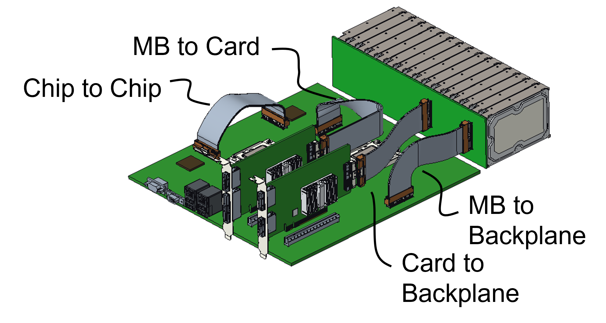
Since each generation of PCIe doubles the data transfer rate, PCI-SIG member companies want copper cabling to help with the design of high-speed PCIe interconnects on a printed circuit board (PCB), between PCBs, and between racks (see diagram).
“We’ve seen a lot of interest over recent months for an optical cable that will support PCI Express,” says Al Yanes, PCI-SIG president and chairperson.
He cites the trends of the decreasing cost and size of optics and how silicon photonics enables the adding of optics alongside ASICs.
“We have formed a workgroup to deliver an optical cable,” says Yanes. “There are many applications, but one is a longer-distance reach for PCI Express.”
“It is a void in the market [the lack of optical support for PCIe], and it needs to be filled,” says Bill Koss, CEO of Drut Technologies. “These efforts tend to take longer than estimated, so better to start sooner.”
Drut has developed a PCIe over photonics solution as part of its photonic direct connect fabric for the data centre.
The data centre is going photonic, says Koss, so there is a need for such working standards as photonics get closer to processors.
The PCIe protocol
PCIe is used widely across many industries.
In the data centre, PCIe is used by general-purpose microprocessors and accelerator chips, such as FPGAs, graphics processing units and AI hardware, to connect to storage and network interface cards.
The PCIe bus uses point-to-point communications based on a simple duplex scheme – serial transmissions in both directions which is referred to as a lane.
The bus can be bundled in various lane configurations – x1, x2, x4, x8, x12, x16 and x32 – with x4, x8 and x16 the configurations most used.
The first two PCIe versions, 1.0 and 2.0, delivered 2.5 and 5 giga transfers-per-second (GT/s) per lane per direction, respectively.
A transfer refers to an encoded bit. The first two PCIe versions use an 8b/10b encoding scheme such that for every ten-bit payload sent, 8 bits are data. This is why the data transfer rates per lane per direction are 2Gbps and 4Gbps (250 and 500 gigabytes per second), respectively.
With PCIe 3.0, the decision was made to increase the transfer rate to 8GT/s per lane, which assumed that no equalisation would be needed to counter inter-symbol interference at that speed. However, equalisation was required, which explains why PCIe 3.0 adopted 8GT/s and not 10GT/s.
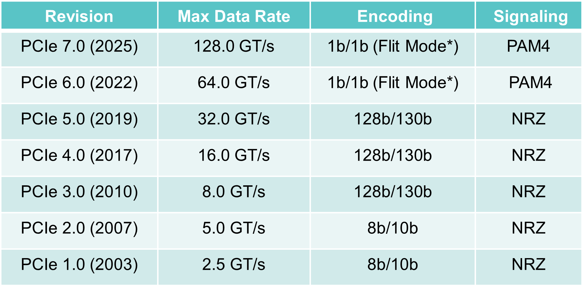
Another PCIe 3.0 decision was to move to a 128b/130b scheme to reduce the encoding overhead from 20 per cent to over 1 per cent. Now the transfer and bit rates are almost equal from the PCIe 3.0 standard onwards.
PCIe 4.0 doubles the transfer rate from 8GT/s to 16GT/s, while PCIe 5.0 is 32GT/s per lane per direction.
Since then, PCIe 6.0 has been specified, supporting 64GT/s per lane per direction. PCIe 6.0 is the first standard for 4-level pulse amplitude modulation (PAM4) signalling.
Now the PCIe 7.0 specification work is at version 0.3. PCIe 7.0 uses PAM-4 to deliver 128GT/s per lane per direction. The standard is expected to be completed in 2025, with industry adoption in 2027.
Optical cabling for PCIe
The PCI Express 5.0 and 6.0 copper cabling specifications are expected by the year-end. The expected distance using copper cabling and retimers is 5-6m.
The reach of an optical PCIe standard will ‘go a lot further’ than that, but how far is to be determined.
Yanes says optical cables for PCIe will also save space: “An optical cable is not as bulky nor as thick as a copper cable.”
Whether the optical specification work will support all versions of PCIe is to be determined.
“There’s some interest to support them all; the copper solution supports all the negotiations,” says Yanes. “It’s something that needs to be discussed, but, for sure, it will be the higher speeds.”
The working group will decide what optical options to specify. “We know that there are some basic things that we need to do to PCI Express technology to make it support optics,” says Yanes.
The working group aims to make the specification work generic enough that it is ‘optical friendly’.
“There are many optical techniques in the industry, and there is discussion as to which of these optical techniques is going to be the winner in terms of usage,” says Yanes. “We want our changes to make PCI Express independent of that discussion.”
The organisation will make the required changes to the base specification of PCIe to suit optical transmission while identifying which optical solutions to address and build.
PCI-SIG will use the same Flit Mode and the same link training, for example, while the potential specification enhancements include coordinating speed transitions to match the optics, making side-band signals in-band, and making the specification more power-efficient given the extended reach.
Pluggable optical modules, active optical cables, on-board optics, co-packaged optics and optical input-output are all optical solutions being considered.
An optical solution for PCIe will also benefit technologies such as Compute Express Link (CXL) and the Non-Volatile Memory Express (NVMe) protocols implemented over PCIe. CXL, as it is adopted more broadly, will likely drive new uses that will need such technology.
The PCIe optical working group will complete the specifications in 12-18 months. Yanes says a quicker working solution may be offered before then.
II-VI’s VCSEL approach for co-packaged optics
Co-packaged optics was a central theme at this year’s OFC show, held in San Diego. But the solutions detailed were primarily using single-mode lasers and fibre.
The firm II-VI is beating a co-packaged optics path using vertical-cavity surface-emitting lasers (VCSELs) and multi-mode fibre while also pursuing single-mode, silicon photonics-based co-packaged optics.
For multi-mode, VCSEL-based co-packaging, II-VI is working with IBM, a collaboration that started as part of a U.S. Advanced Research Projects Agency-Energy (ARPA-E) project to promote energy-saving technologies.
II-VI claims there are significant system benefits using VCSEL-based co-packaged optics. The benefits include lower power, cost and latency when compared with pluggable optics.
The two key design decisions that achieved power savings are the elimination of the retimer chip – also known as a direct-drive or linear interface – and the use of VCSELs.
The approach – what II-VI calls shortwave co-packaged optics – integrates the VCSELs, chip and optics in the same package.
The design is being promoted as first augmenting pluggables and then, as co-packaged optics become established, becoming the predominant solution for system interconnect.
For every 10,000 QSFP-DD pluggable optical modules used by a supercomputer that are replaced with VCSEL-based co-packaged optics, the yearly electricity bill will be reduced by up to half a million dollars, estimate II-VI and IBM.
VCSEL technology
VCSELs are used for active optical cables and short-reach pluggables for up to 70m or 100m links.
VCSEL-based modules consume fewer watts and are cheaper than single-mode pluggables.
Several factors account for the lower cost, says Vipul Bhatt, vice president of marketing, datacom vertical at II-VI.
The VCSEL emits light vertically from its surface, simplifying the laser-fibre alignment, and multi-mode fibre already has a larger-sized core compared to single-mode fibre.
“Having that perpendicular emission from the laser chip makes manufacturing easier,” says Bhatt. “And the device’s small size allows you to get many more per wafer than you can with edge-emitter lasers, benefitting cost.”
The tinier VCSEL also requires a smaller current density to work; the threshold current of a distributed feedback (DFB) laser used with single-mode fibre is 25-30mA, whereas it is 5-6mA for a VCSEL. “That saves power,” says Bhatt.
Fibre plant
Hyperscalers such as Google favour single-mode fibre for their data centres. Single-mode fibre supports longer reach transmissions, while Google sees its use as future-proofing its data centres for higher-speed transmissions.
Chinese firms Alibaba and Tencent use multi-mode fibre but also view single-mode fibre as desirable longer term.
Bhatt says he has been hearing arguments favouring single-mode fibre for years, yet VCSELs continue to advance in speed, from 25 to 50 to 100 gigabits per lane.
“VCSELs continue to lead in cost and power,” says Bhatt. ”And the 100-gigabit-per-lane optical link has a long life ahead of it, not just for networking but machine learning and high-performance computing.“
II-VI says single-mode fibre and silicon photonics modules are suited for the historical IEEE and ITU markets of enterprise and transport where customers have longer-reach applications.
VCSELs are best suited for shorter reaches such as replacing copper interconnects in the data centre.
Copper interconnect reaches are shrinking as interface speeds increase, while a cost-effective optical solution is needed to support short and intermediate spans up to 70 meters.
“As we look to displace copper, we’re looking at 20 meters, 10 meters, or potentially down to three-meter links using active optical cables instead of copper,” says Bhatt. “This is where the power consumption and cost of VCSELs can be an acceptable premium to copper interconnects today, whereas a jump to silicon photonics may be cost-prohibitive.”
Silicon photonics-based optical modules have higher internal optical losses but they deliver reaches of 2km and 10km.
“If all you’re doing is less than 100 meters, think of the incredible efficiency with which these few milliamps of current pumped into a VCSEL and the resulting light launched directly and efficiently into the fibre,” says Bhatt. “That’s an impressive cost and power saving.”
Applications
The bulk of VCSEL sales for the data centre are active optical cables and short-reach optical transceivers.
“Remember, not every data centre is a hyperscale data centre,” says Bhatt. ”So it isn’t true that multi-mode is only for the server to top-of-rack switch links. Hyperscale data centres also have small clusters for artificial intelligence and machine learning.”
The 100m-reach of VCSELs-based optics means it can span all three switching tiers for many data centres.
The currently envisioned 400-gigabit VCSEL modules are 400GBASE-SR8 and the 8-by-50Gbps 400G-SR4.2. Both use 50-gigabit VCSELs: 25 gigabaud devices with 4-level pulse amplitude modulation (PAM-4).
The 400GBASE-SR8 module requires 16 fibres, while the 400G-SR4.2, with its two-wavelength bidirectional design, has eight fibres.
The advent of 100-gigabit VCSELs (50 gigabaud with PAM-4) enables 800G-SR8, 400G-SR4 and 100G-SR1 interfaces. II-VI first demonstrated a 100-gigabit VCSEL at ECOC 2019, while 100-gigabit VCSEL-based modules are becoming commercially available this year.
Terabit VCSEL MSA
The Terabit Bidirectional (BiDi) Multi-Source Agreement (MSA) created earlier this year is tasked with developing optical interfaces using 100-gigabit VCSELs.
The industry consortium will define 800 gigabits interface over parallel multi-mode fibre, the same four pairs of multi-mode fibre that support the 400-gigabit, 400G-BD4.2 interface. It will also define a 1.6 terabit optical interface.
The MSA work will extend the parallel fibre infrastructure from legacy 40 gigabits to 1.6 terabits as data centres embrace 25.6-terabit and soon 51.2-terabit switches.
Founding Terabit BiDi MSA members include II-VI, Alibaba, Arista Networks, Broadcom, Cisco, CommScope, Dell Technologies, HGGenuine, Lumentum, MACOM and Marvell Technology.
200-gigabit lasers and parallelism
The first 200-gigabit electro-absorption modulator lasers (EMLs) were demonstrated at OFC ’22, while the next-generation 200-gigabits directly modulated lasers (DMLs) are still in the lab.
When will 200-gigabit VCSELs arrive?
Bhatt says that while 200-gigabit VCSELs were considered to be research-stage products, recent interest in the industry has spurred the VCSEL makers to accelerate the development timeline.
Bhatt repeats that VCSELs are best suited for optimised short-reach links.
“You have the luxury of making tradeoffs that longer-reach designs don’t have,” he says. “For example, you can go parallel: instead of N-by-200-gig lanes, it may be possible to use twice as many 100-gig lanes.”
VCSEL parallelism for short-reach interconnects is just what II-VI and IBM are doing with shortwave co-packaged optics.
Shortwave co-packaged optics
Computer architectures are undergoing significant change with the emergence of accelerator ICs for CPU offloading.
II-VI cites such developments as Nvidia’s Bluefield data processing units (DPUs) and the OpenCAPI Consortium, which is developing interface technology so that any microprocessor can talk to accelerator and I/O devices.
“We’re looking at how to provide a high-speed, low-latency fabric between compute resources for a cohesive fabric,” says Bhatt. The computational resources include processors and accelerators such as graphic processing units (GPUs) and field-programmable gate arrays (FPGAs).
II-VI claims that by using multi-mode optics, one can produce the lowest power consumption optical link feasible, tailored for very-short electrical link budgets.
The issue with pluggable modules is connecting them to the chip’s high-speed signals across the host printed circuit board (PCB).
“We’re paying a premium to have that electrical signal reach through,” says Bhatt. “And where most of the power consumption and cost are is those expensive chips that compensate these high-speed signals over those trace lengths on the PCB.”
Using shortwave co-packaged optics, the ASIC can be surrounded by VCSEL-based interfaces, reducing the electrical link budget from some 30cm for pluggables to links only 2-3cm long.
“We can eliminate those very expensive 5nm or 7nm ICs, saving money and power,” says Bhatt.
The advantage of shortwave co-packaged optics is better performance (a lower error rate) and lower latency (between 70-100ns) which is significant when connecting to pools of accelerators or memory.
“We can reduce the power from 15W for a QSFP-DD module down to 5W for a link of twice the capacity,” says Bhatt, “We are talking an 80 per cent reduction in power dissipation. Another important point is that when power capacity is finite, every watt saved in interconnects is a watt available to add more servers. And servers bring revenue.”
This is where the 10,000-unit optical interfaces, $0.4-$0.5 million savings in yearly electricity costs comes from.
The power savings arise from the VCSEL’s low drive current, the use of the OIF’s ultra short-reach (USR) electrical interface and the IBM processor driving the VCSEL directly, what is called a linear analogue electrical interface.
In the first co-packaged optics implementation, IBM and II-VI use non-return-to-zero (NRZ) signalling.
The shortwave co-packaged optics has a reach of 20m which enables the potential elimination of top-of-rack switches, further saving costs. (See diagram.)

II-VI sees co-packaged optics as initially augmenting pluggables. With next-generation architectures using 1.6-terabit OSFP-XD pluggables, 20 to 40 per cent of those ports are for sub-20m links.
“We could have 20 to 40 per cent of the switch box populated with shortwave co-packaged optics to provide those links,” says Bhatt.
The remaining ports could be direct-attached copper, longer-reach silicon-photonics modules, or VCSEL modules, providing the flexibility associated with pluggables.
“We think shortwave co-packaged optics augments pluggables by helping to reduce power and cost of next-generation architectures.”
This is the secret sauce of every hyperscaler. They don’t talk about what they’re doing regarding machine learning and their high-performance systems, but that’s where they strive to differentiate their architectures, he says.
Status
Work has now started on a second-generation shortwave design that will use PAM-4 signalling. “That is targeted as a proof-of-concept in the 2024 timeframe,” says Bhatt.
The second generation will enable a direct comparison in terms of power, speed and bandwidth with single-mode co-packaged optics designs.
Meanwhile, II-VI is marketing its first-phase NRZ-based design.
“Since it is an analogue front end, it’s truly rate agnostic,” says Bhatt. “So we’re pitching it as a low-latency, low-power bandwidth density solution for traditional 100-gigabit Ethernet.”
The design also can be used for next-generation PCI Express and CXL disaggregated designs.
II-VI says there is potential to recycle hyperscaler data centre equipment by adding state-of-the-art network fabric to enable pools of legacy processors. “This technology delivers that,” says Bhatt.
But II-VI says the main focus is for accelerator fabrics: proprietary interfaces like NVlink, Fujitsu’s Tofu interconnect or HPE’s Cray’s Slingshot.
“At some point, memory pools or storage pools will also work their way into the hyperscalers’ data centres,” says Bhatt.

Vodafone's effort to get silicon for telco
This as an exciting time for semiconductors, says Santiago Tenorio, which is why his company, Vodafone, wants to exploit this period to benefit the radio access network (RAN), the most costly part of the wireless network for telecom operators.
The telecom operators want greater choice when buying RAN equipment.
As Tenorio, a Vodafone Fellow (the company’s first) and its network architecture director, notes, there were more than ten wireless RAN equipment vendors 15 years ago. Now, in some parts of the world, the choice is down to two.
“We were looking for more choice and that is how [the] Open RAN [initiative] started,” says Tenorio. “We are making a lot of progress on that and creating new options.”
But having more equipment suppliers is not all: the choice of silicon inside the equipment is also limited.
“You may have Fujitsu radios or NEC radios, Samsung radios, Mavenir software, whatever; in the end, it’s all down to a couple of big silicon players, which also supply the incumbents,” he says. “So we thought that if Open RAN is to go all the way, we need to create optionality there too to avoid vendor lock-in.”
Vodafone has set up a 50-strong research team at its new R&D centre in Malaga, Spain, that is working with chip and software companies to develop the architecture of choice for Open RAN to expand the chip options.
Open RAN R&D
Vodafone’s R&D centre’s 50-staff are organised into several streams, but their main goal is to answer critical issues regarding the Open RAN silicon architecture.
“Things like whether the acceleration is in-line or look-aside, which is a current controversy in the industry,” says Tenorio. “These are the people who are going to answer that question.”
With Open RAN, the virtualised Distributed Unit (DU) runs on a server. This contrasts with specialised hardware used in traditional baseband units.
Open RAN processes layer 1 data in one of two ways: look-aside or in-line. With look-aside, the server’s CPU performs certain layer 1 tasks, aided by accelerator hardware to perform tasks like forward error correction. This requires frequent communication between the two that limits processing efficiency.
In-line solves this by performing all the layer 1 processing using a single chip. Dell, for example, has an Open RAN accelerator card that performs in-line processing using Marvell’s silicon.
When Vodafone announced its Open RAN silicon initiative in January, it was working with 20 chip and software companies. More companies have since joined.
“You have software players like middleware suppliers, also clever software plug-ins that optimise the silicon itself,” says Tenorio. “It’s not only silicon makers attracted by this initiative.”
Vodafone has no preconceived ideas as to the ideal solution. “All we want is the best technical solution in terms of performance and cost,” he says.
By performance, Vodafone means power consumption and processing. “With a more efficient solution, you need less [processing] cores,” says Tenorio.
Vodafone is talking to the different players to understand their architectures and points of view and is doing its own research that may include simulations.
Tenorio does not expect Vodafone to manufacture silicon: “I mean, that’s not necessarily on the cards.” But Vodafone must understand what is possible and will conduct lab testing and benchmark measurements.
“We will do some head-to-head measurements that, to be fair, no one I know does,” he says. Vodafone’s position will then be published, it will create a specification and will drive vendors to comply with it.
“We’ve done that in the past,” says Tenorio. “We have been specifying radios for the last 20 years, and we never had to manufacture one; we just needed to understand how they’re done to take the good from the bad and then put everybody on the art of the possible.”
Industry interest
The companies joining Vodafone’s Open RAN chip venture are motivated for different reasons.
Some have joined to ensure that they have a voice and influence Vodafone’s views. “Which is super,” says Tenorio.
Others are there because they are challengers to the current ecosystem. “They want to get the specs ahead of anybody to have a better chance of succeeding if they listen to our advice, which is also super,” says Tenorio.
Meanwhile, software companies have joined to see whether they can improve hardware performance.
“That is the beauty of having the whole ecosystem,” he says.

Work scale
The work is starting at layer 1 and not just the RAN’s distributed unit (DU) but also the radio unit (RU), given how the power amplifier technology is the biggest offender in terms of power consumption.
Layers 2 and 3 will also be tackled. “We’re currently running that on Intel, and we’re finding that there is a lot of room for improvement, which is normal,” says Tenorio. “It’s true that running the three layers on general-purpose hardware has room for improvement.”
That room for improvement is almost equivalent to one full generation of silicon, he says.
Vodafone says that it also can’t be the case that Intel is the only provider of silicon for Open RAN.
The operator expects new hardware variants based on ARM, perhaps AMD, and maybe the RISC-V architecture at some point.
“We will be there to make it happen,” says Tenorio.
Other chip accelerators
Does such hardware as Graphics Processing Units (GPUs), Data Processing Units (DPUs) and also programmable logic have roles?
“I think there’s room for that, particularly at the point that we are in,” says Tenorio. “The future is not decided yet.”
The key is to avoid vendor lock-in for layer 1 acceleration, he says.
He highlights the work of such companies like Marvell and Qualcomm to accelerate layer 1 tasks, but he fears this will drive the software suppliers to take sides on one of these accelerators. “This is not what we want,” he says.
What is required is to standardise the interfaces to abstract the accelerator from the software, or steer away from custom hardware and explore the possibilities of general-purpose but specialised processing units.
“I think the future is still open,” says Tenorio. “Right now, I think people tend to go proprietary at layer 1, but we need another plan.”
“As for FPGAs, that is what we’re trying to run away from,” says Tenorio. “If you are an Open RAN vendor and can’t afford to build your ASIC because you don’t have the volume, then, okay, that’s a problem we were trying to solve.”
Improving general-purpose processing avoids having to go to FPGAs which are bulky, power-hungry and expensive, says Tenorio but he also notes how FPGAs are evolving.
“I don’t think we should have religious views about it,” he says. “There are semi-programmable arrays that are starting to look better and better, and there are different architectures.”
This is why he describes the chip industry as ‘boiling’: “This is the best moment for us to take a view because it’s also true that, to my knowledge, there is no other kind of player in the industry that will offer you a neutral, unbiased view as to what is best for the industry.”
Without that, the fear is that by acquisition and competition, the chip players will reduce the IC choices to a minimum.
“You will end up with two to three incumbent architectures, and you run a risk of those being suboptimal, and of not having enough competition,” says Tenorio.
Vodafone’s initiative is open to companies to participate including its telco competitors.
“There are times when it is faster, and you make a bigger impact if you start things on your own, leading the way,” he says.
Vodafone has done this before: In 2014, it started working with Intel on Open RAN.
“We made some progress, we had some field trials, and in 2017, we approached TIP (the Telecom Infra Project), and we offered to contribute our progress for TIP to continue in a project group,” says Tenorio. “At that point, we felt that we would make more progress with others than going alone.”
Vodafone is already deploying Open RAN in the UK and has said that by 2030, 30 per cent of its deployments in Europe will be Open RAN.
“We’ve started deploying open RAN and it works, the performance is on par with the incumbent architecture, and the cost is also on par,” says Tenorio. “So we are creating that optionality without paying any price in terms of performance, or a huge premium cost, regardless of what is inside the boxes.”
Timeline
Vodafone is already looking at in-line versus look-aside.
“We are closing into in-line benefits for the architecture. There is a continuous flow of positions or deliverables to the companies around us,” says Tenorio. “We have tens of meetings per week with interested companies who want to know and contribute to this, and we are exchanging our views in real-time.”
There will also be a white paper published, but for now, there is no deadline.
But there is an urgency to the work given Vodafone is deploying Open RAN, but this research work is for the next generation of Open RAN. “We are deploying the previous generation,” he says.
Vodafone is also talking, for example, to the ONF open-source organisation, which announced an interest in defining interfaces to exploit acceleration hardware.
“I think the good thing is that the industry is getting it, and we [Vodafone] are just one factor,” says Tenorio. “But you start these conversations, and you see how they’re going places. So people are listening.”
The industry agrees that layer 1 interfacing needs to be standardised or abstracted to avoid companies ending in particular supplier camps.
“I think there’ll be a debate whether that needs to happen in the ORAN Alliance or somewhere else,” says Tenorio. “I don’t have strong views. The industry will decide.”
Other developments
The Malaga R&D site will not just focus on Open RAN but other parts of the network, such as transport.
Transport still makes use of proprietary silicon but there is also more vendor competition.
“The dollars spent by operators in that area is smaller,” says Tenorio. “That’s why it is not making the headlines these days, but that doesn’t mean there is no action.”
Two transport areas where disaggregated designs have started are the disaggregated backbone router, and the disaggregated cell site gateway, both being sensible places to start.
“Disaggregating a full MPLS carrier-grade router is a different thing, but its time will come,” says Tenorio, adding that the centre in Malaga is not just for Open RAN, but silicon for telcos.