
Ciena: Changing bandwidth on the fly
Ciena has announced its latest coherent chipset that will be the foundation for its future optical transmission offerings. The chipset, dubbed WaveLogic 3, will extend the performance of its 100 Gigabit links while introducing transmission flexibility that will trade capacity with reach.
Feature: Beyond 100 Gigabit - Part 1
 "We are going to be deployed, [with WaveLogic 3] running live traffic in many customers’ networks by the end of the year"
Michael Adams, Ciena
"This is changing bandwidth modulation on the fly," says Ron Kline, principal analyst, network infrastructure group at market research firm, Ovum. “The capability will allow users to dynamically optimise wavelengths to match application performance requirements.”
WaveLogic 3 is Ciena's third-generation coherent chipset that introduces several firsts for the company.
- The chipset supports single-carrier 100 Gigabit-per-second (Gbps) transmission in a 50GHz channel.
- The chipset includes a transmit digital signal processor (DSP) - which can adapt the modulation schemes as well as shape the pulses to increase spectral efficiency. The coherent transmitter DSP is the first announced in the industry.
- WaveLogic 3's second chip, the coherent receiver DSP, also includes soft-decision forward error correction (SD-FEC). SD-FEC is important for high-capacity metro and regional, not just long-haul and trans-Pacific routes, says Ciena.
The two-ASIC chipset is implemented using a 32nm CMOS process. According to Ciena, the receiver DSP chip, which compensates for channel impairments, measures 18 mm sq. and is capable of 75 Tera-operations a second.
Ciena says the chipset supports three modulation formats: dual-polarisation bipolar phase-shift keying (DP-BPSK), quadrature phase-shift keying (DP-QPSK) and 16-QAM (quadrature amplitude modulation). Using a single carrier, these equate to 50Gbps, 100Gbps and 200Gbps data rates. Going to 16-QAM may increase the data rate to 200Gbps but it comes at a cost: a loss in spectral efficiency and in reach.
"This software programmability is critical for today's dynamic, cloud-centric networks," says Michael Adams, Ciena’s vice president of product & technology marketing.
WaveLogic 3 has also been designed to scale to 400Gbps. "This is the first programmable coherent technology scalable to 400 Gig," says Adams. "For 400 Gig, we would be using a dual-carrier, dual-polarisation 16-QAM that would use multiple [WaveLogic 3] chipsets."
Performance
Ciena stresses that this is a technology not a product announcement. But it is willing to detail that in a terrestrial network, a single carrier 100Gbps link using WaveLogic 3 can achieve a reach of 2,500+ km. "These refer to a full-fill [wavelengths in the C-Band] and average fibre," says Adams. "This is not a hero test with one wavelength and special [low-loss] fibre.”
 Metro to trans-Pacific: The different reaches and distances over terrestrial and submarine using Ciena's WaveLogic 3. SC stands for single carrier. Source: Ciena/ Gazettabyte
When the modulation is changed to BPSK, the reach is effectively doubled. And Ciena expects a 9,000-10,000km reach on submarine links.
The same single-carrier 50GHz channel reverting to 16-QAM can transmit a 200Gbps signal over distances of 750-1,000km. "A modulation change [to 16-QAM] and adding a second 100 Gigabit Ethernet transceiver and immediately you get an economic improvement," says Adams.
For 400Gbps, two carriers, each 16-QAM, are needed and the distances achieved are 'metro regional', says Ciena.
The transmit DSP also can implement spectral shaping. According to Ciena, by shaping the signals sent, a 20-30% bandwidth improvement (capacity increase) can be achieved. However that feature will only be fully exploited once networks deploy flexible grid ROADMs.
At OFC/NFOEC. Ciena will be showing a prototype card that will demonstrate the modulation going from BPSK to QPSK to 16-QAM. "We are going to be deployed, running live traffic in many customers’ networks by the end of the year," says Adams.
Analysis
Sterling Perrin, senior analyst, Heavy Reading
Heavy Reading believes Ciena's WaveLogic 3 is an impressive development, compared to its current WaveLogic 2 and to other available coherent chipsets. But Perrin thinks the most significant WaveLogic 3 development is Ciena’s single-carrier 100Gbps debut.
Until now, Ciena has used two carriers within a 50GHz, each carrying 50Gbps of data.
"The dual carrier approach gave Ciena a first-to-market advantage at 100Gbps, but we have seen the vendor lose ground as Alcatel-Lucent rolled out its single carrier 100Gbps system," says Perrin in a Heavy Reading research note. "We believe that Alcatel-Lucent was the market leader in 100Gbps transport in 2011."
Other suppliers, including Cisco Systems and Huawei, have also announced single-carrier 100Gbps, and more single-wavelength 100Gbps announcements will come throughout 2012.
Heavy Reading believes the ability to scale to 400Gbps is important, as is the use of multiple carriers (or super-channels). But 400 Gigabit and 1 Terabit transport are still years away and 100Gbps transport will be the core networking technology for a long time yet.
"The vendors with the best 100G systems will be best-positioned to capture share over the next five years, we believe," says Perrin.
Ron Kline, principal analyst for Ovum’s network infrastructure group.
For Ron Kline, Ciena's announcement was less of a surprise. Ciena showcased WaveLogic 3's to analysts late last year. The challenge with such a technology announcement is understanding the capabilities and how it will be rolled out and used within a product, he says.
"Ciena's WaveLogic 3 is the basis for 400 Gig," says Kline. "They are not out there saying 'we have 400 Gig'." Instead, what the company is stressing is the degree of added capacity, intelligence and flexibility that WaveLogic 3 will deliver. That said, Ciena does have trials planned for 400 Gig this year, he says.
What is noteworthy, says Ovum, is that 400Gbps is within Ciena's grasp whereas there are still some vendors yet to record revenues for 100Gbps.
"Product differentiation has changed - it used to be about coherent," says Kline. "But now that nearly all vendors have coherent, differentiation is going to be determined by who has the best coherent technology."
OFC/NFOEC 2012: Technical paper highlights
 Source: The Optical Society
Novel technologies, operators' experiences with state-of-the-art optical deployments and technical papers on topics such as next-generation PON and 400 Gigabit and 1 Terabit optical transmission are some of the highlights of the upcoming OFC/NFOEC conference and exhibition, to be held in Los Angeles from March 4-8, 2012. Here is a taste of some of the technical paper highlights.
Optical networking
In Spectrum, Cost and Energy Efficiency in Fixed-Grid and Flew-Grid Networks (Paper number 1248601) an evaluation of single and multi-carrier networks at rates up to 400 Gigabit-per-second (Gbps) is made by the Athens Information Technology Center. One finding is that efficient spectrum utilisation and fine bit-rate granularity are essential if cost and energy efficiencies are to be realised.
In several invited papers, operators report their experiences with the latest networking technologies. AT&T Labs discusses advanced ROADM networks; NTT details the digital signal processing (DSP) aspects of 100Gbps DWDM systems and, in a separate paper, the challenge for Optical Transport Network (OTN) at 400Gbps and beyond, while Verizon gives an update on the status of MPLS-TP. As part of the invited papers, Finisar's Chris Cole outlines the next-generation CFP modules.
Optical access
Fabrice Bourgart of FT-Orange Labs details where the next generation PON standards - NGPON2 - are going while NeoPhotonics's David Piehler outlines the state of photonic integrated circuit (PIC) technologies for PONS. This is also a topic tackled by Oclaro's Michael Wale: PICs for next-generation optical access systems. Meanwhile Ao Zhang of Fiberhome Telecommunication Technologies discusses the state of FTTH deployments in the world's biggest market, China.
Switching, filtering and interconnect optical devices
NTT has a paper that details a flexible format modulator using a hybrid design based on a planar lightwave circuit (PLC) and lithium niobate. In a separate paper, NTT discusses silica-based PLC transponder aggregators for a colourless, directionless and contentionless ROADM, while Nistica's Tom Strasser discusses gridless ROADMs. Compact thin-film polymer modulators for telecoms is a subject tackled by GigOptix's Raluca Dinu.
One novel paper is on graphene-based optical modulators by Ming Liu, Xiang at the UC Berkeley (Paper Number: 1249064). The optical loss of graphene can be tuned by shifting its Fermi level, he says. The paper shows that such tuning can be used for a high-speed optical modulator at telecom wavelengths.
Optoelectronic Devices
CMOS photonic integrated circuits is the topic discussed by MIT's Rajeev Ram, who outlines a system-on-chip with photonic input and output. Applications range from multiprocessor interconnects to coherent communications (Paper Number: 1249068).
A polarisation-diversity coherent receiver on polymer PLC for QPSK and QAM signals is presented by Thomas Richter of the Fraunhofer Institute for Telecommunications (Paper Number: 1249427). The device has been tested in systems using 16-QAM and QPSK modulation up to 112 Gbps.
Core network
Ciena's Maurice O'Sullivan outlines 400Gbps/ 1Tbps high-spectral efficiency technology and some of the enabling subsystems. Alcatel-Lucent's Steven Korotky discusses traffic trends: drivers and measures of cost-effective and energy-efficient technologies and architectures for the optical backbone networks, while transport requirements for next-generation heterogeneous networks is the subject tackled by Bruce Nelson of Juniper Networks.
Data centre
IBM's Casimir DeCusatis presents a future - 2015-and-beyond - view of data centre optical networking. The data centre is also tackled by HP's Moray McLaren, in his paper on future computing architectures enabled by optical and nanophotonic interconnects. Optically-interconnected data centres are also discussed by Lei Xu of NEC Labs America.
Expanding usable capacity of fibre syposium
There is a special symposium at OFC/ NFOEC entitled Enabling Technologies for Fiber Capacities Beyond 100 Terabits/second. The papers in the symposium discuss MIMO and OFDM, technologies more commonly encountered in the wireless world.
2012: The year of 100 Gigabit transponders
 “The world is moving to coherent, there is no question about that”
Per Hansen, Oclaro
The 100Gbps module expands the company's coherent offerings. Oclaro is already shipping a 40Gbps coherent module. “The world is moving to coherent, there is no question about that,” says Per Hansen, vice president of product marketing, optical networks solutions at Oclaro.
Why is this significant?
Having a selection of 100Gbps long-haul optical modules will aid the uptake of high-capacity links in the network core. Opnext announced in September its OTM-100 100Gbps coherent optical module, in production from April 2012. And at least one other module maker has worked with ADVA Optical Networking to make its 100Gbps module, a non-coherent design.
The 100Gbps coherent optical modules will enable system vendors without their own technology to enter the marketplace. It also presents those system vendors with their own 100Gbps technology - the likes of Alcatel-Lucent, Ciena, Cisco and Huawei - with a dilemma: do they continue to evolve their products or embrace optical modules?
“These system vendors have developed [100Gbps] in-house to have a strategic differentiator," says Hansen. "But with lower volumes you have a higher cost.” The advent of 100Gbps modules diminishes the strategic advantage of in-house technology while enabling system vendors to benefit from cheaper, more broadly available modules, he says.
What has been done
Oclaro is still developing the MI 8000XM module and has yet to reveal the reach performance of the module: “We want to do many more tests before we share,” says Hansen. The module will meet the Optical Internetworking Forum's (OIF) 100Gbps module maximum power consumption limit of 80W, he says.
 The OIF 100 Gigabit module architecture
The NEL DSP chip is the same device that Opnext is using for its 100Gbps module. “A partnership agreement and sourcing arrangement with NEL allows us to come to market with what we think is a very good product at the right time,” says Hansen.
The DSP uses soft-decision forward error correction. Opnext has said this adds 2-3dB to the optical performance to achieve a reach of 1500-1600km before regeneration.
In 2010 Oclaro announced it had invested US $7.5 million in Clariphy Communications as part of the chip company's development of its 100Gbps coherent receiver chip, the CL10010. As part of the agreement, Oclaro will get a degree of exclusivity as a module supplier (at least one other module maker will also benefit).
ClariPhy has said that while it will not be first to market with a 100Gbps ASIC, the CL10010 will be a 28nm CMOS second-generation chip design. To be able to enter the market with a 100Gbps module next year, Oclaro adopted NEL's design which exists now.
Next
Hansen says that the MI 8000XM, which uses a lithium niobate modulator, is designed to achieve maximum reach and optical performance. But future 100Gbps modules will be developed that may use other modulator technologies and be optimised in terms of power or size.
Hansen is also in no doubt that the next speed hike after 100Gbps will be 400Gbps. Like 100Gbps, there will be some early-adopter operators that embrace the technology one or two years before the consensus.
Such a development is still several years away, however, since an industry standard for 400Gbps must be developed which is only expected in 2014 only.
Intelligent networking: Q&A with Alcatel-Lucent's CTO
Alcatel-Lucent's corporate CTO, Marcus Weldon, in a Q&A with Gazettabyte. Here, in Part 1, he talks about the future of the network, why developing in-house ASICs is important and why Bell Labs is researching quantum computing.
 Marcus Weldon (left) with Jonathan Segel, executive director in the corporate CTO Group, holding the lightRadio cube. Photo: Denise Panyik-Dale
Q: The last decade has seen the emergence of Asian Pacific players. In Asia, engineers’ wages are lower while the scale of R&D there is hugely impressive. How is Alcatel-Lucent, active across a broad range of telecom segments, ensuring it remains competitive?
A: Obviously we have a Chinese presence ourselves and also in India. It varies by division but probably half of our workforce in R&D is in what you would consider a low-cost country. We are already heavily present in those areas and that speaks to the wage issue.
But we have decided to use the best global talent. This has been a trait of Bell Labs in particular but also of the company. We believe one of our strengths is the global nature of our R&D. We have educational disciplines from different countries, and different expertise and engineering foci etc. Some of the Eastern European nations are very strong in maths, engineering and device design. So if you combine the best of those with the entrepreneurship of the US, you end up with a very strong mix of an R&D population that allows for the greatest degree of innovation.
We have no intention to go further towards a low-cost country model. There was a tendency for that a couple of years ago but we have pulled back as we found that we were losing our innovation potential.
We are happy with the mix we have even though the average salary is higher as a result. And if you take government subsidies into account in European nations, you can get almost the same rate for a European engineer as for a Chinese engineer, as far as Alcatel-Lucent is concerned.
One more thing, Chinese university students, interestingly, work so hard up to getting into university that university is a period where they actually slack off. There are several articles in the media about this. The four years that students spend in university, away from home for the first time, they tend to relax.
Chinese companies were complaining that the quality of engineers out of university was ever decreasing because of what was essentially a slacker generation, they were arguing, of overworked high-school students that relaxed at college. Chinese companies found that they had to retrain these people once employed to bring them to the level needed.
So that is another small effect which you could argue is a benefit of not being in China for some of our R&D.
Alcatel-Lucent's Bell Labs: Can you spotlight noteworthy examples of research work being done?
Certainly the lightRadio cube stuff is pure Bell Labs. The adaptive antenna array design, to give you an example, was done between the US - Bell Labs' Murray Hill - and Stuttgart, so two non-Asian sites at Bell Labs involved in the innovations. These are wideband designs that can operate at any frequencies and are technology agnostic so they can operate for GSM, 3G and LTE (Long Term Evolution).
"We believe that next-generation network intelligence, 10-15 years from now, might rely on quantum computing"
The designs can also form beams so you can be very power-efficient. Power efficiency in the antenna is great as you want to put the power where it is needed and not just have omni (directional) as the default power distribution. You want to form beams where capacity is needed.
That is clearly a big part of what Bell Labs has been focussing on in the wireless domain as well as all the overlaying technologies that allow you to do beam-forming. The power amplifier efficiency, that is another way you lose power and you operate at a more costly operational expense. The magic inside that is another focus of Bell Labs on wireless.
In optics, it is moving from 100 Gig to 400 Gig coherent. We are one of the early innovators in 100 Gig coherent and we are now moving forward to higher-order modulation and 400 Gig.
On the DSL side it the vectoring/ crosstalk cancellation work where we have developed our own ASIC because the market could not meet the need we had. The algorithms ended up producing a component that will be in the first release of our products to maintain a market advantage.
We do see a need for some specialised devices like the FlexPath FP3 network processor, the IPTV product, the OTN (Optical Transport Network) switch that is at the heart of our optical products is our own ASIC, and the vectoring/ crosstalk cancellation engine in our DSL products. Those are the innovations Bell Labs comes up with and very often they lead to our portfolio innovations.
There is also a lot of novel stuff like quantum computing that is on the fringes of what people think telecoms is going to leverage but we are still active in some of those forward-looking disciplines.
We have quite a few researchers working on quantum computing, leveraging some of the material expertise that we have to fabricate novel designs in our lab and then create little quantum computing structures.
Why would quantum computing be useful in telecom?
It is very good for parsing and pattern matching. So when you are doing complex searches or analyses, then quantum computing comes to the fore.
We do believe there will be processing that will benefit from quantum computing constructs to make decisions in ever-increasingly intelligent networks. Quantum computing has certain advantages in terms of its ability to recognise complex states and do complex calculations. We believe that next-generation network intelligence, 10-15 years from now, might rely on quantum computing.
We don't have a clear application in mind other than we believe it is a very important space that we need to be pioneering.
"Operators realise that their real-estate resource - including down to the central office - is not the burden that it appeared to be a couple of years ago but a tremendous asset"
You wrote a recent blog on the future of the network. You mentioned the idea of the emergence of one network with the melding of wireless and wireline, and that this will halve the total cost of ownership. This is impressive but is it enough?
The half number relates to the lightRadio architecture. There are many ingredients in it. The most notable is that traffic growth is accounted for in that halving of the total cost of ownership. We calculated what the likely traffic demand would be going forward: a 30-fold increase in five years.
Based on that growth, when we computed how much the lightRadio architecture, involving the adaptive antenna arrays, small cells and the move to LTE, if you combine these things and map it into traffic demand, the number comes up that you can build the network for that traffic demand and with those new technologies and still halve the total cost of ownership.
It really is quite a bit more aggressive than it appears because it is taking account of a very significant growth in traffic.
Can we build that network and still lower the cost? The answer is yes.
You also say that intelligence will be increasingly distributed in the network, taking advantage of Moore's Law. This raises two questions. First, when does it make sense to make your own ASICs?
When I say ASICs I include FPGAs. FPGAs are your own design just on programmable silicon and normally you evolve that to an ASIC design once you get to the right volumes.
There is a thing called an NRE (non-recurring engineering) cost, a non-refundable engineering cost to product an ASIC in a fab. So you have to have a certain volume that makes it worthwhile to produce that ASIC, rather than keeping it in an FPGA which is a more expensive component because it is programmable and has excess logic. On the other hand, there is economics that says an FPGA is the right way for sub-10,000 volumes per annum whereas for millions of parts you would do an ASIC.
We work on both those types of designs. And generally, and I think even Huawei would agree with us, a lot of the early innovation is done in FPGAs because you are still playing with the feature set.
 Photo: Denise Panyik-Dale
Often there is no standard at that point, there may be preliminary work that is ongoing, so you do the initial innovation pre-standard using FPGAs. You use a DSP or FPGA that can implement a brand new function that no one has thought of, and that is what Bell Labs will do. Then, as it starts becoming of interest to the standard bodies, you have it implemented in a way that tries to follow what the standard will be, and you stay in a FPGA for that process. At some point later, you take a bet that the functionality is fixed and the volume will be high enough, and you move to an ASIC.
So it is fairly commonplace for novel technology to be implemented by the [system] vendors. And only in the end stage when it has become commoditised to move to commercial silicon, meaning a Broadcom or a Marvell.
Also around the novel components we produce there are a whole host of commercial silicon components from Texas Instruments, Broadcom, Marvell, Vitesse and all those others. So we focus on the components where the magic is, where innovation is still high and where you can't produce the same performance from a commercial part. That is where we produce our own FPGAs and ASICs.
Is this trend becoming more prevalent? And if so, is it because of the increasing distribution of intelligence in network.
I think it is but only partly because of intelligence. The other part is speed. We are reaching the real edges of processing speed and generally the commercial parts are not at that nanometer of [CMOS process] technology that can keep up.
To give an example, our FlexPath processor for the router product we have is on 40nm technology. Generally ASICs are a technology generation behind FPGAs. To get the power footprint and the packet-processing performance we need, you can't do that with commercial components. You can do it in a very high-end FPGA but those devices are generally very expensive because they have extremely low yields. They can cost hundreds or thousands of dollars.
The tendency is to use FPGAs for the initial design but very quickly move to an ASIC because those [FGPA] parts are so rare and expensive; nor do they have the power footprint that you want. So if you are running at very high speeds - 100Gbps, 400Gbps - you run very hot, it is a very costly part and you quickly move to an ASIC.
Because of intelligence [in the network] we need to be making our own parts but again you can implement intelligence in FPGAs. The drive to ASICs is due to power footprint, performance at very high speeds and to some extent protection of intellectual property.
FPGAs can be reverse-engineered so there is some trend to use ASICs to protect against loss of intellectual property to less salubrious members of the industry.
Second, how will intelligence impact the photonic layer in particular?
You have all these dimensions you can trade off each other. There are things like flexible bit-rate optics, flexible modulation schemes to accommodate that, there is the intelligence of soft-decision FEC (forward error correction) where you are squeezing more out of a channel but not just making it a hard-decision FEC - is it a '0' or a '1' but giving a hint to the decoder as to whether it is likely to be a '0' or a '1'. And that improves your signal-to-noise ratio which allows you to go further with a given optics.
So you have several intelligent elements that you are going to co-ordinate to have an adaptive optical layer.
I do think that is the largest area.
Another area is smart or next-generation ROADMs - we call it connectionless, contentionless, and directionless.
There is a sense that as you start distributing resources in the network - cacheing resources and computing resources - there will be far more meshing in the metro network. There will be a need to route traffic optically to locally positioned resources - highly distributed data centre resources - and so there will be more photonic switching of traffic. Think of it as photonic offload to a local resource.
We are increasingly seeing operators realise that their real-estate resource - including down to the central office - is not the burden that it appeared to be a couple of years ago but a tremendous asset if you want to operate a private cloud infrastructure and offer it as a service, as you are closer to the user with lower latency and more guaranteed performance.
So if you think about that infrastructure, with highly distributed processing resources and offloading that at the photonic layer, essentially you can easily recognise that traffic needs to go to that location. You can argue that there will be more photonic switching at the edge because you don't need to route that traffic, it is going to one destination only.
This is an extension of the whole idea of converged backbone architecture we have, with interworking between the IP and optical domains, you don't route traffic that you don't need to route. If you know it is going to a peering point, you can keep that traffic in the optical domain and not send it up through the routing core and have it constantly routed when you know from the start where it is going.
So as you distribute computing and cacheing resources, you would offload in the optical layer rather than attempt to packet process everything.
There are smarts at that level too - photonic switching - as well as the intelligent photonic layer.
For the second part of the Q&A, click here
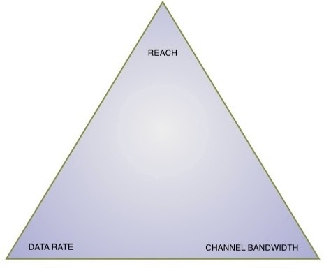
The great data rate-reach-capacity tradeoff
 Source: Gazettabyte
Optical transmission technology is starting to bump into fundamental limits, resulting in a three-way tradeoff between data rate, reach and channel bandwidth. So says Brandon Collings, JDS Uniphase's CTO for communications and commercial optical products. See the recent Q&A.
This tradeoff will impact the coming transmission speeds of 200, 400 Gigabit-per-second and 1 Terabit-per-second. For each increased data rate, either the channel bandwidth must increase or the reach must decrease or both, says Collings.
Thus a 200Gbps light path can be squeezed into a 50GHz channel in the C-band but its reach will not match that of 100Gbps over a 50GHz channel (Shown on the graph with a hashed line). A wider version of 200Gbps could match the reach to the 100Gbps, but that would probably need a 75GHz channel, says Collings.
For 400Gbps, the same situation arises suggesting two possible approaches: 400Gbps fitting in a 75GHz channel but with limited reach (for metro) or a 400Gbps signal placed within a 125GHz channel to match the reach of 100Gbps over a 50GHz channel.
 Optical transmission technology is starting to bump into fundamental limits resulting in a three-way tradeoff between data rate, reach and channel bandwidth.
"Continue this argument for 1 Terabit as well," says Collings. Here the industry consensus suggests a 200GHz-wide channel will be needed.
Similarly, within this compromise, other options are available such as 400Gbps over a 50GHz channel. But this would have a very limited reach.
Collings does not dismiss the possibility of a technology development which would break this fundamental compromise, but at present this is the situation.
As a result there will likely be multiple formats hitting the market which align the reach needed with the minimised channel bandwidth, says Collings.
Fujitsu Labs adds processing to boost optical reach

“That is one of the virtues of the technology; it is not dependent on the modulation format or the bit rate”
Takeshi Hoshida, Fujitsu Labs
Why is it important?
Much progress has been made in developing digital signal processing techniques for 100Gbps coherent receivers to compensate for undesirable fibre transmission effects such as polarisation mode dispersion and chromatic dispersion (See Performance of Dual-Polarization QPSK for Optical Transport Systems). Both dispersions are linear in nature and are compensated for using linear digital filtering. What Fujitsu Labs has announced is the next step: a digital filter design that compensates for non-linear effects.
A key challenge facing optical-transmission designers is extending the reach of 100Gbps transmissions to match that of 10Gbps systems. In the simplest sense, reach falls with increased transmission speed because the shorter-pulsed signals contain less photons. Channel impairments also become more prominent the higher the transmission speed.
Engineers can increase system reach by boosting the optical signal-to-noise ratio but this gives rise to non-linear effects in the fibre. “When the signal power is higher, the refractive index of the fibre changes and that distorts the phase of the optical signal,” says Takeshi Hoshida, a senior researcher at Fujitsu Labs.
The non-linear effect, combined with polarisation mode dispersion and chromatic dispersion, interact with the signal in a complicated way. “The linear and non-linear effects combine to result in a very complex distortion of the received signal,” says Hoshida.
Fujitsu has developed a non-linear distortion compensation technique that recovers 2dB of the transmitted optical signal. Moreover, the compensation technique will equally benefit 400 Gigabit or 1 Terabit channels, says Hoshida: “That is one of the virtues of the technology; it is not dependent on the modulation format or the bit rate.”
Fujitsu plans to extend the reach of its long-haul optical transmission systems using the technique. The 2dB equates to a 1.6x distance improvement. But, as Hoshida points out, this is the theoretical benefit. In practice, the benefit is less since a greater transmission distance means the signal passes through more amplifier and optical add-drop stages that introduce their own signal impairments.
Method used
Fujitsu Labs has implemented a two-stage filtering block. The first filter stage is linear and compensates for chromatic dispersion, while the second unit counteracts the fibre's non-linear effect on the optical signal. To achieve the required compensation, Fujitsu Labs uses multiple filter-stage blocks in cascade.
According to Hoshida, optical phase is rotated according to the optical power: “If the power is higher, the more phase rotation occurs – that is the non-linear effect in the fibre.” The effect is distributed, occurring along the length of the fibre, and is also coupled with chromatic dispersion. “Chromatic dispersion changes the optical intensity waveform, and that intensity waveform induces the non-linear effect,” says Hoshida. “Those two problems are coupled to each other so you have to solve both.”
Fujitsu tackles the problem by applying a filter stage to compensate for each optical span – the fibre segment between repeaters. For a terrestrial transmission system there can be as many as 20 or 30 such spans. “But [using a filter stage per span] is rather inefficient,” says Hoshida. By inserting a weighted-average technique, Fujitsu has reduced by a factor of four the filter stages needed.
Weighted-averaging is a filtering operation that smoothes the signal in the time domain. “It is not necessary to change the weights [of the filter] symbol-by-symbol; it is almost static,” says Hoshida. Changes do occur but infrequently, depending on the fibre’s condition such as changes in temperature, for example.
Fujitsu has been surprised that the weighted-averaging technique is so effective. The technique’s use and the subsequent 4x reduction in filter stages reduce by 70% the hardware needed to implement the compensation. The reason it is not the full 75% is that extra hardware for the weighted averaging must be added to each stage.
What next?
Fujitsu has demonstrated that the technique is technically feasible but practical issues remain such as power consumption. According to Hoshida, the power consumption is too high even using an advanced 40nm CMOS process, and will likely require a 28nm process. Fujitsu thus expects the technique to be deployed in commercial systems by 2015 at the latest.
There are also further optical performance improvements to be claimed, says Hoshida, by addressing cross-phase modulation. This is another non-linear effect where one lightpath affects the phase of another.
Fujitsu Labs has developed two algorithms to address cross-phase modulation which is a more challenging problem since it is modulation-dependent.
For a copy of Fujitsu’s ECOC 2010 slides, please click here.
Optical transmission beyond 100Gbps
Part 3: What's next?
Given the 100 Gigabit-per-second (Gbps) optical transmission market is only expected to take off from 2013, addressing what comes next seems premature. Yet operators and system vendors have been discussing just this issue for at least six months.
And while it is far too early to talk of industry consensus, all agree that optical transmission is becoming increasingly complex. As Karen Liu, vice president, components and video technologies at market research firm Ovum, observed at OFC 2010, bandwidth on the fibre is no longer plentiful.
 “We need to keep a very close eye that we are not creating more problems than we are solving.”
Brandon Collings, JDS Uniphase.
As to how best to extend a fibre’s capacity beyond 80, 100Gbps dense wavelength division multiplexing (DWDM) channels spaced 50GHz apart, all options are open.
“What comes after 100Gbps is an extremely complicated question,” says Brandon Collings, CTO of JDS Uniphase’s consumer and commercial optical products division. “It smells like it will entail every aspect of network engineering.”
Ciena believes that if operators are to exploit future high-speed transmission schemes, new architected links will be needed. The rigid networking constraints imposed on 40 and 100Gbps to operate over existing 10Gbps networks will need to be scrapped.
“It will involve a much broader consideration in the way you build optical systems,” says Joe Berthold, Ciena’s vice president of network architecture. “For the next step it is not possible [to use existing 10Gbps links]; no-one can magically make it happen.”
Lightpaths faster than 100Gbps simply cannot match the performance of current optical systems when passing through multiple reconfigurable optical add/drop multiplexer (ROADM) stages using existing amplifier chains and 50GHz channels.
Increasing traffic capacity thus implies re-architecting DWDM links. “Whatever the solution is it will have to be cheap,” says Berthold. This explains why the Optical Internetworking Forum (OIF) has already started a work group comprising operators and vendors to align objectives for line rates above 100Gbps.
If new links are put in then changing the amplifier types and even their spacing becomes possible, as is the use of newer fibre. “If you stay with conventional EDFAs and dispersion managed links, you will not reach ultimate performance,” says Jörg-Peter Elbers, vice president, advanced technology at ADVA Optical Networking,
Capacity-boosting techniques
Achieve higher speeds while matching the reach of current links will require a mixture of techniques. Besides redesigning the links, modulation schemes can be extended and new approaches used such as going ‘gridless” and exploiting sophisticated forward error-correction (FEC) schemes.
For 100Gbps, polarisation and phase modulation in the form of dual polarization, quadrature phase-shift keying (DP-QPSK) is used. By adding amplitude modulation, quadrature amplitude modulation (QAM) schemes can be extended to include 16-QAM, 64-QAM and even 256 QAM.
Alcatel-Lucent is one firm already exploring QAM schemes but describes improving spectral efficiency using such schemes as a law of diminishing returns. For example, 448Gbps based on 64-QAM achieves a bandwidth of 37GHz and a sampling rate of 74 Gsamples/s but requires use of high-resolution A/D converters. “This is very, very challenging,” says Sam Bucci, vice president, optical portfolio management at Alcatel-Lucent.
Infinera is also eyeing QAM to extend the data performance of its 10-channel photonic integrated circuits (PICs). Its roadmap goes from today’s 100Gbps to 4Tbps per PIC.
Infinera has already announced a 10x40Gbps PIC and says it can squeeze 160 such channels in the C-band using 25GHz channel spacing. To achieve 1 Terabit would require a 10x100Gbps PIC.
How would it get to 2Tbps and 4Tbps? “Using advanced modulation technology; climbing up the QAM ladder,” says Drew Perkins, Infinera’s CTO.
Glenn Wellbrock, director of backbone network design at Verizon Business, says it is already very active in exploring rates beyond 100Gbps as any future rate will have a huge impact on the infrastructure. “No one expects ultra-long-haul at greater than 100Gbps using 16-QAM,” says Wellbrock.
Another modulation approach being considered is orthogonal frequency-division multiplexing (OFDM). “At 100Gbps, OFDM and the single-carrier approach [DP-QPSK] have the same spectral efficiency,” says Jonathan Lacey, CEO of Ofidium. “But with OFDM, it’s easy to take the next step in spectral efficiency – required for higher data rates - and it has higher tolerance to filtering and polarisation-dependent loss.”
One idea under consideration is going “gridless”, eliminating the standard ITU wavelength grid altogether or using different sized bands, each made up of increments of narrow 25GHz ones. “This is just in the discussion phase so both options are possible,” says Berthold, who estimates that a gridless approach promises up to 30 percent extra bandwidth.
Berthold favours using channel ‘quanta’ rather than adopting a fully flexibility band scheme - using a 37GHz window followed by a 17GHz window, for example - as the latter approach will likely reduce technology choice and lead to higher costs.
Wellbrock says coarse filtering would be needed using a gridless approach as capturing the complete C-Band would be too noisy. A band 5 or 6 channels wide would be grabbed and the signal of interest recovered by tuning to the desired spectrum using a coherent receiver’s tunable laser, similar to how a radio receiver works.
Wellbrock says considerable technical progress is needed for the scheme to achieve a reach of 1500km or greater.
 “Whatever the solution is it will have to be cheap”
Joe Berthold, Ciena.
JDS Uniphase’s Collings sounds a cautionary note about going gridless. “50GHz is nailed down – the number of questions asked that need to be addressed once you go gridless balloons,” he says. “This is very complex; we need to keep a very close eye that we are not creating more problems than we are solving.”
“Operators such as AT&T and Verizon have invested heavily in 50GHz ROADMs, they are not just going to ditch them,” adds Chris Clarke, vice president strategy and chief engineer at Oclaro.
More powerful FEC schemes and in particular soft-decision FEC (SD-FEC) will also benefit optical performance for data rates above 100Gbps. SD-FEC delivers up to a 1.3dB coding gain improvement compared to traditional FEC schemes at 100Gbps.
SD-FEC also paves the way for performing joint iterative FEC decoding and signal equalisation at the coherent receiver, promising further performance improvements, albeit at the expense of a more complex digital signal processor design.
400Gbps or 1 Tbps?
Even the question of what the next data rate after 100Gbps will be –200Gbps, 400Gbps or even 1 Terabit-per -second – remains unresolved.
Verizon Business will deploy new 100Gbps coherent-optimised routes from 2011 and would like as much clarity as possible so that such routes are future-proofed. But Collings points out that this is not something that will stop a carrier addressing immediate requirements. “Do they make hard choices that will give something up today?” he says.
At the OFC Executive Forum, Verizon Business expressed a preference for 1Tbps lightpaths. While 400Gbps was a safe bet, going to 1Tbps would enable skipping one additional stage i.e. 400Gbps. But Verizon recognises that backing 1Tbps depends on when such technology would be available and at what cost.
According to BT, speeds such as 200, 400Gbps and even 1 Tbps are all being considered. “The 200/ 400Gbps systems may happen using multiple QAM modulation,” says Russell Davey, core transport Layer 1 design manager at BT. “Some work is already being done at 1Tbps per wavelength although an alternative might be groups or bands of wavelengths carrying a continuous 1Tbps channel, such as ten 100Gbps wavelengths or five 200Gbps wavelengths.”
Davey stresses that the industry shouldn’t assume that bit rates will continue to climb. Multiple wavelengths at lower bitrates or even multiple fibres for short distances will continue to have a role. “We see it as a mixed economy – the different technologies likely to have a role in different parts of network,” says Davey.
Niall Robinson, vice president of product marketing at Mintera, is confident that 400Gbps will be the chosen rate.
Traditionally Ethernet has grown at 10x rates while SONET/SDH has grown in four-fold increments. However now that Ethernet is a line side technology there is no reason to expect the continued faster growth rate, he says. “Every five years the line rate has increased four-fold; it has been that way for a long time,” says Robinson. “100Gbps will start in 2012/ 2013 and 400Gbps in 2017.”
“There is a lot of momentum for 400Gbps but we’ll have a better idea in a six months’ time,” says Matt Traverso, senior manager, technical marketing at Opnext. “The IEEE [and its choice for the next Gigabit Ethernet speed after 100GbE] will be the final arbiter.”
Software defined optics and cognitive optics
Optical transmission could ultimately borrow two concepts already being embraced by the wireless world: software defined radio (SDR) and cognitive radio.
SDR refers to how a system can be reconfigured in software to implement the most suitable radio protocol. In optical it would mean making the transmitter and receiver software-programmable so that various transmission schemes, data rates and wavelength ranges could be used. “You would set up the optical transmitter and receiver to make best use of the available bandwidth,” says ADVA Optical Networking’s Elbers.
This is an idea also highlighted by Nokia Siemens Networks, trading capacity with reach based on modifying the amount of information placed on a carrier.
“For a certain frequency you can put either one bit [of information] or several,” says Oliver Jahreis, head of product line management, DWDM at Nokia Siemens Networks. “If you want more capacity you put more information on a frequency but at a lower signal-to-noise ratio and you can’t go as far.”
Using ‘cognitive optics’, the approach would be chosen by the optical system itself using the best transmission scheme dependent capacity, distance and performance constraints as well as the other lightpaths on the fibre. “You would get rid of fixed wavelengths and bit rates altogether,” says Elbers.
Market realities
Ovum’s view is it remains too early to call the next rate following 100Gbps.
Other analysts agree. “Gridless is interesting stuff but from a commercial standpoint it is not relevant at this time,” says Andrew Schmitt, directing analyst, optical at Infonetics Research.
Given that market research firms look five years ahead and the next speed hike is only expected from 2017, such a stance is understandable.
Optical module makers highlight the huge amount of work still to be done. There is also a concern that the benefits of corralling the industry around coherent DP-QPSK at 100Gbps to avoid the mistakes made at 40Gbps will be undone with any future data rate due to the choice of options available.
Even if the industry were to align on a common option, developing the technology at the right price point will be highly challenging.
“Many people in the early days of 100Gbps – in 2007 – said: ‘We need 100Gbps now – if I had it I’d buy it’,” says Rafik Ward, vice president of marketing at Finisar. “There should be a lot of pent up demand [now].” The reason why there isn’t is that such end users always miss out key wording at the end, says Ward: “If I had it I’d buy it - at the right price.”
For Part 1, click here
For Part 2, click here