
OFC 2014 industry reflections - Part 2

The high cost of 100 Gigabit Ethernet client modules has been a major disappointment to me as it has slowed adoption
Joe Berthold, Ciena
Joe Berthold, vice president of network architecture at Ciena.
OFC 2014 was another great event, with interesting programmes, demonstrations and papers presented. A few topics that really grabbed my interest were discussions around silicon photonics, software-defined networking (SDN) and 400 Gigabit Ethernet (GbE).
The intense interest we saw at last year’s OFC around silicon photonics grew this year with lots of good papers and standing-room-only sessions. I look forward to future product announcements that deliver on the potential of this technology to significantly reduce cost of interconnecting systems over modest distances. The high cost of 100GbE client modules has been a major disappointment to me as it has slowed adoption.
Another area of interest at this year’s show was the great deal of experimental work around SDN, some more practical than others.
I particularly liked the reviews of the latest work under the DARPA-sponsored CORONET programme, whose Phase 3 focused on SDN control of multi-layer, multi-vendor, multi-data centre cloud networking across wide area networks.
In particular, there were talks from three companies I noted: Anne Von Lehman of Applied Communication Sciences, the prime contractor, provided a good program overview; Bob Doverspike of AT&T described a very extensive testbed using equipment of the type currently deployed in AT&T’s network, as well as two different processing and storage virtualisation platforms; and Doug Freimuth of IBM described its contributions to CORONET including an OpenStack virtualisation environment, as well as other IBM distributed cloud networking research.
All the action on rates above 100 Gig lies with the selection of client signals. 400 Gig seems to have the major mindshare but there are still calls for flexible rate clients and Terabit clients.
One thing I enjoyed about these talks was that they described an approach to SDN for distributed data centre networking that is pragmatic and could be realised soon.
I also really liked a workshop held on the Sunday on the question whether SDN will kill GMPLS. While there was broad consensus that GMPLS has failed in delivering on its original turn-of-the-century vision of IP routers control of multi-layer, multi-domain networks, most speakers recognised the value distributed control planes have in simplifying and speeding the control of single layer, single domain networks.
What I took away was that single layer distributed control planes are here to stay as important network control functions, but instead will work under the direction of an SDN network controller.
As we all know, 400 Gigabit dense wavelength division multiplexing (DWDM) is here from the technology perspective, but awaiting standardisation of the 400 Gig Ethernet signal from the IEEE, and follow-on work by the ITU-T on signal mapping to OTN. In fact, from the perspective of DWDM transmission systems, 1 Terabit-per-second systems can be had for the asking.
All the action on rates above 100 Gig lies with the selection of client signals. 400 Gig seems to have the major mindshare but there are still calls for flexible rate clients and Terabit clients.
One area that received a lot of attention, with many differing points of view, was the question of the 400GbE client. As the 400GbE project begins soon in the IEEE, it is time to take a lesson from the history of the 100 Gig client modules and do better.
Let us all agree that we don’t need 400 Gig clients until they can do better in cost, face plate density, and power dissipation than the best 100 Gig modules that will exist then.
The first 100 Gig DWDM transceivers were introduced in 2009. It is now 2014 and 100 Gig is the transmission rate of choice for virtually all high capacity DWDM network applications, with a strong economic value proposition versus 10 Gig. Yet the industry has not yet managed to achieve cost/bit parity between 100 Gig and 10 Gig clients - far from it!
Last year's OFC, we saw many show floor demonstrations of CFP2 modules. They promise lower costs, but evidence of their presence in shipping products is still lacking. At the exhibit this year we saw 100 Gig QSFP28 modules. While progress is slow, the cost of the 100 Gig client module continues to result in many operators favouring 10 Gig handoffs to their 100 Gig optical networking systems.
Let us all agree that we don’t need 400 Gig clients until they can do better in cost, face plate density, and power dissipation than the best 100 Gig modules that will exist then. At this juncture the 100 Gig benchmark we should be comparing 400 Gig to is a QSFP28 package.
Lastly, last year we heard about the launch of an OIF project to create a pluggable analogue coherent optical module. There were several talks that referenced this project, and discussed its implications for shrinking size and supporting higher transceiver card density.
Broad adoption of this component will help drive down costs of coherent transceivers, so I look forward to its hearing about its progress at OFC 2015.
Daryl Inniss, vice president and practice leader, Ovum.
There was no shortage of client-side announcements at OFC and I’ve spent time since the conference trying to organise them and understand what it all means.
I’m tempted to say that the market is once again developing too many options and not quickly agreeing on a common solution. But I’m reminded that this market works collaboratively and the client-side uncertainty we’re seeing today is a reflection of a lack of market clarity.
Let me describe three forces affecting suppliers:
The IEEE 100GBASE-xxx standards represent the best collective information that suppliers have. Not surprisingly, most vendors brought solutions to OFC supporting these standards. Vendors sharpened their products and focused on delivering solutions with smaller form factors and lower power consumption. Advances in optical components (lasers, TOSAs and ROSAs), integrated circuits (CDRs, TIAs, drivers), transceivers, active optical cables, and optical engines were all presented. A promising and robust supply base is emerging that should serve the market well.
A second driver is that hyperscale service providers want a cost-effective solution today that supports 500m to 2km. This is non-standard and suppliers have not agreed on the best approach. This is where the market becomes fragmented. The same vendors supporting the IEEE standard are also pushing non-standard solutions. There are at least four different approaches to support the hyperscale request:
- Parallel single mode (PSM4) where an MSA was established in January 2014
- Coarse wavelength division multiplexing—using uncooled directly modulated lasers and single mode fibre
- Dense wavelength division multiplexing—this one just emerged on the scene at OFC with Ranovus and Mellanox introducing the OpenOptics MSA
- Complex modulation—PAM-8 for example and carrier multi-tone.
Admittedly, the presence of this demand disrupts the traditional process. But I believe the suppliers’ behavior reflects their unhappiness with the standardisation solution.
The good news is these approaches are using established form factors like the QSFP. And silicon photonic products are starting to emerge. Suppliers will continue to innovate.
Ambiguity will persist but we believe that clarity will ultimately prevail.
The third issue lurking in the background is knowledge that 400 Gig and one Terabit will soon be needed. The best-case scenario is to use 100 Gig as a platform to support the next generation. Some argue for complex modulation as you reduce the number of optical components thereby lowering cost. That’s good but part of the price is higher power consumption, an issue that is to be determined.
Part of today’s uncertainty is whether the standard solution is suitable to support the market to the next generation. Sixteen channels at 25 Gig is doable but feels more like a stopgap measure than a long-term solution.
These forces leave suppliers innovating in search of the best path forward. The approaches and solutions differ for each vendor. Timing is an issue too with hyperscale looking for solutions today while the mass market may be years away.
We believe that servers with 25 Gig and/ or 40 Gig ports will be one of the catalysts to drive the mass market and this will not start until about 2016. Meanwhile, each vendor and the market will battle for the apparent best solution to meet the varying demands. Ambiguity will persist but we believe that clarity will ultimately prevail.
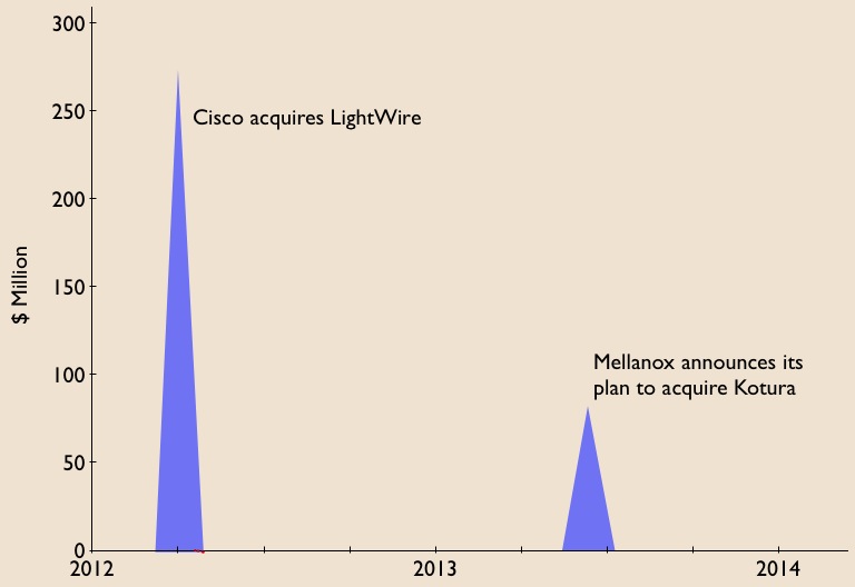
Mellanox to acquire silicon photonics player Kotura
 Source: Gazettabyte
Mellanox Technologies has announced its intention to acquire silicon photonics player, Kotura, for $82 million.
The acquisition will enable Mellanox to deliver 100 Gigabit Infiniband and Ethernet interconnect in the coming two years. lt will also provide Kotura with the resources needed to bring its 100 Gigabit QSFP to market. Mellanox will also gain Kotura's optical engine for use in active optical cables and new mid-plane platform designs, as well as future higher speed interfaces.
The news is also significant for the optical component industry. Kotura is one of the three established merchant silicon photonics players - the others being LightWire and Luxtera - that have spent years developing their technologies.
LightWire was acquired by Cisco Systems in March 2012 for US $271 million and now Mellanox plans to acquire Kotura. The two equipment vendors recognise the value of the technology, bringing it in-house to reduce system interconnect costs and as a long term differentiator for their equipment and ASIC designs. Mellanox, as a silicon photonics player, will compete with Intel, with its own silicon photonics technology, and Cisco Systems.
Kotura has been using its technology to sell telecom products such as variable optical attenuators and multiplexers. The start-up recently announced its 100 Gig QSFP that uses wavelength division multiplexing (WDM) transmitter and receiver chips. The product is to become available in 2014.
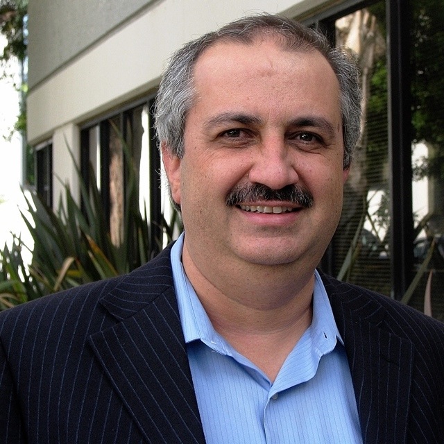
In an interview last year, Kotura's CTO, Mehdi Asghari, discussed a roadmap showing how its 100 Gigabit silicon photonics technology could scale to 400 Gigabit and eventually 1.6 Terabit.
"Our devices are capable of running at 40 or 50 Gigabit-per-second (Gbps), depending on the electronics. The electronics is going to limit the speed of our devices. We can very easily see going from four channels at 25Gbps to 16 channels at 25Gbps to provide a 400 Gigabit solution," Asghari told Gazettabyte.
Kotura also discussed how the line rate could be increased to 50Gbps either using a non-return-to-zero (NRZ) line rate or using a multi-level modulation such as pulse amplitude modulation (PAM).
"To get to 1.6 Terabit transceivers, we envisage something running at 40Gbps times 40 channels or 50Gbps times 32 channels. We already have done a single receiver chip demonstrator that has 40 channels, each at 40Gbps," said Asghari.
"These things in silicon are not a big deal. The III-V guys really struggle with yield and cost. But you can envisage scaling to that level of complexity in a silicon platform."
Silicon photonics will not replace existing VCSEL or indium phosphide-based transceiver designs. But there is no doubting silicon photonics is emerging as a key optical technology and the segment is heating up.
If the early start-ups are being acquired, there have been more recent silicon photonics players entering the marketplace such as Aurrion, Skorpios Technologies and Teraxion. There are also internal developments among equipment players such as Alcatel-Lucent, HP Labs and IBM. Indeed Kotura has worked closely with Oracle (Sun Microsystems)
Further acquisitions of silicon photonic players should be expected as companies start designing next generation, denser systems and adopt 100 Gigabit and faster interfaces.
Equally, established optical component and module companies will likely enter quietly (and not so quietly) the marketplace adding silicon photonics to their technology toolkits when the timing is right.
Trends to watch
Two industry trends are underway regarding silicon photonics.
The first is system vendors wanting to own the technology to reduce their costs while recognising a need to control and understand the technology as they tackle more complex equipment designs.
The other, what at first glance is a contrarian trend, is the democratisation of silicon photonics.
The technology is slowly passing from the select few to become more generally available for industry use. For this to happen, the relevant design tools need to mature as do third-party fabrication plants that will manufacture the silicon photonics designs.
Appendix:
On June 4th, 2013, Mellanox announced a definitive agreement to acquire chip company IPtronics for $47.5 million as it builds out its in-house technologies for optical interconnect. Click here
Futher reading:
Avago to acquire CyOptics, click here
Silicon photonics: Q&A with Kotura's CTO
A Q&A with Mehdi Asghari, CTO of silicon photonics start-up, Kotura. In part one, Asghari talks about a recent IEEE conference he co-chaired that included silicon photonics, the next Ethernet standard, and the merits of silicon photonics for system design.
Part 1
"Photons and electrons are like cats and dogs. Electrons are dogs: they behave, they stick by you, they are loyal, they do exactly as you tell them, whereas cats are their own animals and they do what they like. And that is what photons are like."
Mehdi Asghari, CTO of Kotura
Q: You recently co-chaired the IEEE International Conference on Group IV Photonics that included silicon photonics. What developments and trends would you highlight?
A: This year I wanted to show that silicon photonics was ready to make a leap from an active area of scientific research to a platform for engineering innovation and product development.
To this end, I needed to show that the ecosystem was ready and present. Therefore, a key objective was to get the industry more involved with the conference. "This has always been a challenge," I was told.
To address this issue I asked my co-chair, MIT's Professor Jurgen Michel, that we appoint joint-session chairs, one from industry and one from academia. We got people we knew from Google, Oracle and Intel as co-chairs, and paired them with prominent academics and asked them to ensure that there were an equal number of industry-invited talks in the schedule. We knew this would be a major attraction to industry attendees. We also got the industry to fund the conference at a level that set an IEEE record.
A key highlight of the show was a boat cruise journey on San Diego bay with Dr. Andrew Rickman as speaker, sharing his experiences and thoughts about setting up the first silicon photonics company - Bookham Technology - over 20 years ago.
Among other distinguished industry speakers we had Samsung telling us of the role of silicon photonics in consumer applications, Broadcom on the need for on-chip optical communication, Cisco on the role of silicon photonics in the future of the Internet, and Google on its broadband fibre-to-the-home (FTTh) initiative and what silicon photonics could offer in this area.
Oracle also shared its latest development in silicon photonics and the application of the technology in their systems, while Luxtera discussed the latest developments in its CMOS photonics platform, particularly the 4x25 Gigabit-per-second (Gbps) platform.
We also heard about the latest germanium laser development at MIT and had an invited speaker to talk about what III-V devices could do and to provide a comparison to silicon to make sure we are not blinded by our own rhetoric.
We ended up with a record number of attendees for the conference and, perhaps more importantly, close to half from industry; a record and vindicated my motivation and perspective for the conference and that silicon photonics is ready and coming.
Was there a trend or presentation at the IEEE event that stood out?
There are two areas creating excitement. One is the germanium laser. This is a topic of significant interest because these devices can operate at very high temperatures and therefore they can be next to the processor or ASIC. This can be a game-changer in how we envisage photonics and electronics being integrated.
We have germanium detectors and at Kotura we are working very hard to get a germanium electro-absorption modulator. We have shown this device can be extremely small and low power. And it can operate at very high speed - we have observed 3dB bandwidths in excess of 70GHz which means you can think of 100 Gigabit direct modulation for a device only 40 microns long and with a capacitance of a few femtofarads. So in terms of RF power, the dissipation of this device is virtually zero.
I would say the MIT group is probably leading the [germanium laser] efforts. They reported on room-temperature, current-driven laser emission which is very exciting. The efficiency of these lasers are still low for commercial applications; they probably have to improve by a factor of 100 or so. But given the progress we've seen in the last two years, if they keep going at that pace we may have viable germanium lasers in a couple of years. Then someone in industry has to take that on and turn it into a product and that is usually the hardest part.
This is exciting because that enables us to forget about off-the-chip lasers and integrate them in the device. We can then give up a whole bunch of problems. For example, the high temperature operation of the III-V devices is a real limit for us. Electronic devices can give off 100W and operate at 120oC, whereas optical devices often have to be stabilised, may go through multiple packaging layers, and the heat dissipation is usually directly related to cost.
If you could end up with a germanium laser that is happy at high temperatures - and we know our detectors and modulators work at high temperatures, and we know we can use electronic packaging to package these devices - then we can put these lasers next to the processor and address the bandwidth limitations that ASICs are facing today.
"Wavelength division multiplexing (WDM) is effectively a zero-power gearbox"
What was the second area?
The other area that was very interesting is graphene, a new material people are starting to work with and putting on silicon. They [researchers] are showing very low power, very high speed operation. It is still at a research level but that is another area we should watch.
The IEEE has started a group looking at the next speed Ethernet standard. No technical specification has been mentioned but it looks that 400 Gigabit Ethernet (GbE) will be the approach. Do you agree and what role can silicon photonics play in making the next speed Ethernet standard possible?
Industry is busy arguing about the different ways of doing 100 and 400GbE, and perhaps forgetting the fact that we have been here before.
The simple fact is that people always go for higher bit rate when it is cost-efficient and power-efficient to do so. After that, wavelengths are used.
Wavelength division multiplexing (WDM) is effectively a zero-power 'gearbox', mixing the signals in the optical domain. You do pay a power penalty for it in the form of photons lost in the multiplexer and demultiplexer. However that is not significant compared to the power consumption of an electronics gearbox chip.
Once we have exploited line rate and wavelength division multiplexing, we come to more complex modulation formats and pay the associated power and complexity penalty. Of course, more channels of fibre can always carry more information bandwidth but that is just a brute force solution that works while density and bandwidth requirements are moderate.
I think the right 100 Gigabit is based on a WDM 4x25 Gig solution. This can then scale to 400 Gigabit by adding more wavelengths, and can then scale to 1.6 Terabits. We have already demonstrated this in a single chip and will demonstrate this later in the form of a QSFP 100Gbps.
How does the interface scale to 1.6Tbps?
Our devices are capable of running at 40 or 50Gbps, depending on the electronics. The electronics is going to limit the speed of our devices. We can very easily see going from four channels at 25Gbps to 16 channels at 25Gbps to provide a 400 Gigabit solution.
We can also see a way of increasing the line rate to 50Gbps perhaps, either a straightforward NRZ (non-return-to-zero) line rate or some people are talking about multi-level modulation, PAM-4 (pulse amplitude modulation) type of stuff, to get to 50Gbps.
The customers we are talking to about 100Gbps are already talking about 400Gbps. So we can see 16x25Gbps, or 8x50Gbps if that is the right thing to do at the time based on the availability of electronics.
To go to 1.6 Terabit transceivers, we envisage something running at 40Gbps times 40 channels or 50Gbps times 32 channels. We already have done a single receiver chip demonstrator that has 40 channels, each at 40Gbps.
These things in silicon are not a big deal. The III-V guys really struggle with yield and cost. But you can envisage scaling to that level of complexity in a silicon platform.
Silicon photonics is spoken of not just as an optical platform like traditional optical integration technologies, but also as a design approach, making use of techniques associated with semiconductor design. The implication is that the technology will enable designs and even systems in a way that traditional optics can't. Can you explain how silicon photonics is a design approach and just what the implications are?
I think this is a key promise of silicon photonics, but perhaps one that has been oversold in recent years.
The key here is that given the maturity of the silicon processing capabilities, process simulation tools available and inherent properties of silicon, it is possible to predict the performance of the optical circuits far better in this platform than in any other before it. I think this is true and very valuable, potentially even a game changer.
However, we have to realise that there still remains an inherent difference between electrons and photons and their behavior in such circuits. Photons remain in a quantum world in such circuits, where the wavelength of light is comparable to feature sizes we manufacture. Hence we are dealing with a statistical quantum process whether we like it or not.
In summary, silicon will be a key enabler for on-chip system design, but it is too early for the university courses to stop graduating photonics PhDs!
So there is an advantage to silicon photonics but are you saying it is not that simple as using mature semiconductor design techniques?
Photons and electrons are like cats and dogs. Electrons are dogs: they behave, they stick by you, they are loyal, they do exactly as you tell them, whereas cats are their own animals and they do what they like. And that is what photons are like.
So it is really hard to predict what a photon does. The dimensions that we use for the structures we make are of the size of the wavelength of a photon. And that means it is more of a hit-and-miss process - there is always stray light, the stray light has a habit of interfering and you can always get unpredicted results.
When I interact with my electronic partners I find that they go through 6-9 months of very detailed simulation. They have very complex simulation tools.
When you come to photonics for sure we can borrow some of these simulation tools, we can simulate the process because we are using silicon. However some of the tolerances that we need are beyond what the silicon guys need, and the way the photons behave is very different. So in the end we don't spend 9 months simulating; we spend a month simulating and 3 months running the process and optimising it and re-running it and re-optimising it.
We end up with a reverse situation where the design is only 3 months, and the interaction with the designer and the manufacturing process is a 9-month process. So this is more of an iterative process. It is not as mature and a little bit more statistical.
Luxtera's 100 Gigabit silicon photonics chip
Luxtera has detailed a 4x28 Gigabit optical transceiver chip. The silicon photonics company is aiming the device at embedded applications such as system backplanes and high-performance computing (HPC). The chip is also being used by Molex for 100 Gigabit active optical cables. Molex bought Luxtera's active optical cable business in January 2011.

“Do I want to invest in a copper backplane for a single generation or do I switch over now to optics and have a future-proof three-generation chassis?”
Marek Tlalka, Luxtera
What has been done
To make the optical transceiver, a distributed-feedback (DFB) laser operating at 1490nm is coupled to the silicon photonics CMOS-based chip. One laser only is required to serve the four individually modulated 28Gbps transmit channels, giving the chip a 112Gbps maximum data rate. There are also four receive channels, each using a germanium-based photo-detector that is grown on-chip.
The DFB is the same laser that Luxtera uses for its 4x10Gbps and 4x14Gbps designs. What has been changed is the Mach-Zehnder waveguide-based modulators that must now operate at 28Gbps, and the electronics amplifiers at the receivers. “The chip [at 5mmx6mm] is pretty much the same size as our 4x10 and 4x14 Gig designs,” says Marek Tlalka, director of marketing at Luxtera.
 Source: Luxtera
Luxtera is announcing the 100 Gigabit chip which it is sampling to customers. Molex, for example, will package the chip and the laser to make its active optical cable products. Luxtera will package the transceiver chip and laser in a housing as an OptoPHY, a packaged product it already provides at lower speeds. The company will sell the 100Gbps OptoPHY for embedded applications such as system backplanes and HPC.
Applications
The 100GbE transceiver chip is targeted at next-generation backplane applications as well as active optical cables. And it is enterprise vendors that make switches, routers and blade servers that are considering adopting optical backplanes for their next-generation platforms, says Luxtera.
According to Tlalka, system vendors are moving their backplanes from 15Gbps to 28Gbps: “It is pretty obvious that building an electrical backplane at this data rate will be extremely challenging.”
When vendors design a new chassis, they want it to support three generations of line cards. Even if a system vendor develops a 28Gbps copper-based backplane, it will need to go optical when the backplane data rate increases to 40-50Gbps in 2-3 years’ time and 100Gbps when that speed transition occurs. “Do I want to invest in a copper backplane for a single generation or do I switch over now to optics and have a future-proof three-generation chassis?” says Tlalka.
Exascale computers, 1000x more powerful than existing supercomputers planned for the second half of the decade, is another application area. Here there is a need for 25-28Gbps links between chips, says Tlalka.
System platforms and HPC are ideal candidates for the packaged transceiver chip but longer term Luxtera is eyeing the move of optics inside chips such as ASICs. Such system-on-chip optical integration could include Ethernet switch ICs (See example switch ICs from Broadcom and Intel (Fulcrum)) and network interface cards. Another example highlighted by Tlalka is CPU-memory interfaces.
However such applications are at least five years away and there are significant hurdles to be overcome. These include resolving the business model of such designs as well as the technical challenges of coupling the ASIC to the optics and the associated mechanical design.
Standards
Luxtera's 100Gbps transceiver chip supports a variety of standards.
Operating at 25Gbps per channel, the chip supports 100GbE and Enhanced Data Rate (EDR) Infiniband. The ability to go to 28Gbps per channel means that the transceiver can also support the OTN (optical transport network) standard as well as proprietary backplane protocols that add overhead to the basic 25Gbps data rate.
In addition the chip supports the OIF's short reach and very short reach interfaces that define the interface between an ASIC and the optical module.
The chip is also suited for some of the IEEE Next Generation 100Gbps Optical Ethernet Study Group standards now in development. These interfaces will cover a reach of 30m to 2km.
400GbE and HDR Infiniband
Luxtera says that it is working on different channel ’flavours' of 100G. It is also following developments such as Infiniband Hexadecimal Data Rate (HDR) and 400GbE.
HDR will use 40Gbps channels while there is still an industry debate as to whether 400GbE will be implemented using ten channels, each at 40Gbps, or as a 16x25Gbps design.