
Silicon photonics grapples with 3D packaging demands
Hesham Taha (pictured), CEO of start-up Teramount, is more upbeat about silicon photonics than ever. But, as he outlines, challenges remain.
Hesham Taha is putting in the miles. The CEO of Teramount has been travelling to the East and West to meet with companies.
Termount is working closely with customers and partners adopting its technology that adds fibre to silicon photonics chips.
“We’re shipping units to customers and partners, and we need to be close to them as they integrate our components and address the challenges of integration,” says Taha.
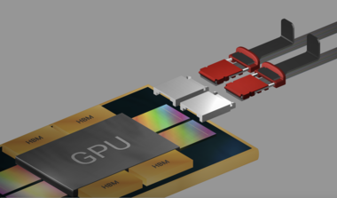
Teramount
For Taha, connecting fibre to a silicon photonics chip inside a pluggable optical transceiver is relatively straightforward.
Far more challenging is when the optical engine and chip are packaged together, known as co-packaged optics. Such a tight coupling raises reliability challenges.
The optical engine is close to the large, heat-generating chip, introducing manufacturing and reliability issues. Also, the fibre-connect to the optical engine inside the package must be scalable. Scaling is key because with each chip generation – whether an AI accelerator or a switch chip – the input-output (I/O) requirements grow.
Teramount’s technology couples the fibre to the silicon photonics chip using a photonic plug and photonic bump.
The photonic plug holds the fibres and couples them to the silicon photonics chip via a photonic bump, a component made during the silicon photonics wafer’s processing.
The photonic bump has two elements: a wideband deflector and a lens mirror for beam expansion. Expanding the light beam enables larger assembly tolerances.
The resulting wafer-level manufacturing may be more complicated, says Taha, but the benefits include relaxed tolerances in the assembly, wideband surface coupling, and the testing of the wafer and the die.
The photonic bump-and-plug combination also enables detachable optics for co-packaged optics designs, benefitting their manufacturing. (For more about Teramount’s technology, click here)
Silicon Photonics meets semiconductor thinking
Taha sees silicon photonics as a platform that enables the integration of optical functions at the wafer scale using standard semiconductor manufacturing techniques.
“It [silicon photonics design] has the same way of thinking as semiconductor people: chip designers, foundries, and packaging people,” says Taha. The result is that silicon photonics is bringing optics to chip design.
The growing maturity of the technology, and the emergence of foundries such as TSMC, GlobalFoundries, Tower Semiconductor, Intel, and ST Microelectronics offering silicon photonics, means that companies with photonic designs can be fabless; a model that has benefitted the chip industry.
Photonic chip designers can use a large foundry’s process design kit (PDK) and send off their silicon photonics designs to be manufactured in volume.
As for co-packaged optics, Taha sees it as a key in the evolution of silicon photonics. Co-package optics is the realisation of silicon photonics whereby optics is integrated next to advanced semiconductor chips.
Industry developments
The growing interest in silicon photonic and co-packaged optics is also evident in some recent announcements, driven by the AI compute scaling needs.
ST Microelectronics unveiled its 300mm wafer PIC100 silicon photonics technology. ST Microelectronics was active in silicon photonics 10 years ago and has returned due to the AI opportunity.
Marvell announced it offers a co-packaged optics solution for accelerator chips to address scale-up networking for AI architectures.
Leading foundry TSMC has outlined its silicon photonics roadmap, which includes co-packaged optics.
And at the GTC 2025 AI developers conference, Nvidia announced it is adding co-packaged optics to its switch platforms for scale-out networking.
“All this is not a surprise because this is where we expected silicon photonics to be one day when we founded the company 10 years ago,” says Taha. “It is just that this day is happening now.”
Teramount sees its fibre attach product as a part of an emerging ecosystem to enable standard semiconductor high-volume manufacturing.
This ecosystem comprises chip designers, foundries, OSATs [outsourced semiconductor assembly and test service providers], and system integrators.
But there are challenges. There may be wafer-scale manufacturing, but issues remain on the integration-packaging side.
“This is why we need to travel, to align with the different partners,” says Taha.
Challenges
Teramount is seeing challenges first-hand given its fibre-attach vantage point. Taha also highlights commercial issues still to be resolved.
The technical challenges revolve around integrating the silicon photonics die with the accompanying lasers and fibres in an advanced package.
Unlike a traditional pluggable optical transceiver, the silicon photonics chip is inserted in a hot environment and must meet operational temperatures of 85oC and even 105oC.
Multiple reflow soldering steps during manufacturing expose the packaging to even higher temperatures (270oC) and thermal stresses.
“These are new technical challenges that silicon photonic chip integration must meet 3D packaging requirements,” says Taha.
3D packaging has requirements that affect the fibre attach. For example, the silicon photonics chip is thinner than the die used in a pluggable if through-silicon via (TSV) technology is used.
TSV refers to the way a vertical electrical connector is done that passes through the die. Any mechanical stresses or warpage impacts the resulting optical performance of the die.
“Co-package optics is creating new challenges when connecting fibre to such thinner chips,” says Taha.
There are also issues with testing a design. “There are still no mature solutions for parallel optical and electrical testing,” says Taha.
The commercial issue he highlights centres around design ownership. With a pluggable module, all the components are delivered in one assembled device with one owner – the module maker.
With co-packaged optics, there are several stages of assembly, with components coming from multiple sources. “Who owns it?” says Taha.
Box system integrators making servers, switches, and the like don’t work with fibre. In contrast, co-packaged optics require connecting and managing hundreds of fibres that fit in a tight space. Good optical coupling and performance are a must to ensure the overall design.
“So this flow [for co-package optics] has yet to be set,” says Taha.
He says all the players, chip designers, foundry packaging vendors (OSATs), and system integrators still need to be aligned. That said, the industry, particularly the large silicon chip vendors, are working to make it happen, says Taha.
This implies that companies such as Nvidia, Intel, AMD, Broadcom, and Marvell are playing a key role here.
Given how the emerging AI opportunity is driving their chip businesses, they have every reason to make this work.

ST makes its first PSM4 optical engine deliveries
What gives Benetti confidence is the demand he is seeing for 100-gigabit transceivers in the data centre. “From my visibility today, the tipping point is 2016,” says Benetti, group vice president and general manager, digital and mixed processes ASIC division at STMicroelectronics.
 Flavio Benetti
Benetti and colleagues at ST have spent the last four years working to bring to market the silicon photonics technology that the chip company licensed from Luxtera.
The company has developed a 300mm-wafer silicon photonics production line at its fabrication plant in Crolles that is now up and running. ST also has its first silicon photonics product - a mid-reach PSM4 100-gigabit optical engine - and has just started its very first deliveries.
At the OFC show in March, ST said it had already delivered samples to one unnamed 'customer partner', possibly Luxtera, and Benetti showed a slide of the PSM4 chips as part of a Lumentum transceiver.
Another ST achievement Benetti highlights is the development of a complete supply chain for the technology. In addition to wafer production, ST has developed electro-optic wafer testing. This allows devices to be probed electrically and optically to select working designs before the wafer is diced. ST has also developed a process to 3D-bond chips.
“We have focussed on building an industrial environment, with a supply chain that can deliver hundreds of thousands and millions of devices,” says Benetti.
PSM4 and CWDM4
ST’s first product, the components for a 4x25 gigabit PSM4 transceiver, is a two-chip design.
One chip is the silicon photonics optical engine which integrates the PSM4’s four modulators, four detectors and the grating couplers used to interface the chip to the fibres. The second chip, fabricated using ST’s 55nm BiCMOS process, houses the transceiver’s associated electronics such as the drivers, and trans-impedance amplifiers.
The two chips are combined using 3D packaging. “The 3D packaging consists of the two dies, one copper-pillar bonded to the other,” says Benetti. “It is a dramatic simplification of the mounting process of an optical module.”
The company is also developing a 100-gigabit CWDM4 transceiver which unlike the PSM4 uses four 25-gigabit wavelengths on a single fibre.
The CWDM4 product will be developed using two designs. The first is an interim, hybrid solution that uses an external planar lightwave circuit-based multiplexer and demultiplexer, followed by an integrated silicon photonics design. The hybrid design is being developed and is expected in late 2017; the integrated silicon photonics design is due in 2018.
With the hybrid design, it is not just a question of adding a mux-demux to the PSM4 design. “The four channels are each carrying a different wavelength so there are some changes that need to be done to the PSM4,” says Benetti, adding that ST is working with partners that will provide the mux-demux and do the integration.
We need to have a 100-gigabit solution in high volume for the market, and the pricing pressure that is coming has convinced us that silicon photonics is the right thing to do
Opportunities
Despite the growing demand for 100-gigabit transceivers that ST is seeing, Benetti stresses that these are not 'mobile-phone wafer volumes'. “We are much more limited in terms of wafers,” he says. Accordingly, there is probably only room for one or two large fabs for silicon photonics globally, in his opinion.
So why is ST investing in a large production line? For Benetti, this is an obvious development for the company which has been a provider of electrical ICs for the optical module industry for years.
“ST has entered silicon photonics to provide our customers with a roadmap,” says Benetti. “We need to have a 100-gigabit solution in high volume for the market, and the pricing pressure that is coming has convinced us that silicon photonics is the right thing to do.”
It also offers chip players the possibility of increasing its revenues. “The optical engine integrates all the components that were in the old-fashioned modules so we can increase our revenues there,” he says.
ST is tracking developments for 200-gigabit and 400-gigabit links and is assessing whether there is enough of an opportunity to justify pursuing 200-gigabit interconnects.
For now though, it is seeing strong pricing pressure for 100-gigabit links for reaches of several hundred meters. “We do not think we can compete for very short reach distances,” says Benetti. “We will leave that to VCSELs until the technology can no longer follow.” As link speeds increase, the reach of VCSEL links diminishes. “We will see more room for silicon photonics but this is not the case in the short term,” says Benetti.
Market promise
People have been waiting for years for silicon photonics to become a reality, says Benetti. “My target is to demonstrate it [silicon photonics] is possible, that we are serious in delivering parts to the market in an industrial way and in volumes that have not been delivered before.”
To convince the market, it is not just showing the technological advantages of silicon photonics but the fact that there is a great simplification in constructing the optical module along with the ability to deliver devices in volume. “This is the point,” he says.
Benetti’s other role at ST is overseeing advanced networking ASICs. He argues that over the mid- to long-term, there needs to be a convergence between ASIC and optical connectivity.
“Look at a switch board, for example, you have a big ASIC or two in the middle and a bunch of optical modes on the side,” says Benetti. For him, the two technologies - photonics and ICs - are complementary and the industry’s challenge is to make the two live together in an efficient way.
Optical integration and silicon photonics: A view to 2021
LightCounting’s report on photonic integration has several notable findings. The first is that only one in 40 optical components sold in the datacom and telecom markets is an integrated device yet such components account for a third of total revenues.

Another finding is that silicon photonics will not have a significant market impact in the next five years to 2021, although its size will grow threefold in that time.
By 2021, one in 10 optical components will be integrated and will account for 40% of the total market, while silicon photonics will become a $1 billion industry by then.
Integrated optics
“Contrary to the expectation that integration is helping to reduce the cost of components, it is only being used for very high-end products,” says Vladimir Kozlov, CEO of LightCounting.
He cites the example of the cost-conscious fibre-to-the-home market which despite boasting 100 million units in 2015 - the highest volumes in any one market - uses discrete parts for its transceivers. “There is very little need for optical integration in this high-volume, low-cost market,” he says
Where integration is finding success is where it benefits device functionality. “Where it takes the scale of components to the next level, meaning much more sophisticated designs than just co-packaged discrete parts,” says Kozlov. And it is because optical integration is being applied to high-end, costlier components that explains why revenues are high despite volumes being only 2.4% of the total market.
Defining integration
LightCounting is liberal in its definition of an integrated component. An electro-absorption modulated laser (EML) where the laser and modulator are on the same chip is considered as an integrated device. “It was developed 20 years ago but is just reaching prime time now with line rates going to 25 gigabit,” says Kozlov.
Designs that integrate multiple laser chips into a transceiver such as a 4x10 gigabit design is also considered an integrated design. “There is some level of integration; it is more sophisticated than four TO-cans,” says Kozlov. “But you could argue it is borderline co-packaging.”
LightCounting forecasts that integrated products will continue to be used for high-end designs in the coming five years. This runs counter to the theory of technological disruption where new technologies are embraced at the low end first before going on to dominate a market.
“We see it continuing to enter the market for high-end products simply because there is no need for integration for very simple optical parts,” says Kozlov.
Silicon photonics
LightCounting does not view silicon photonics as a disruptive technology but Kozlov acknowledges that while the technology has performance disadvantages compared to traditional technologies such as indium phosphide and gallium arsenide, its optical performance is continually improving. “That may still be consistent with the theory of technological disruption,” he says.
There are all these concerns about challenges but silicon photonics does have a chance to be really great
The market is also developing in a way that plays to silicon photonics’ strengths. One such development is the need for higher-speed interfaces, driven by large-scale data centre players such as Microsoft. “Their appetite increases as the industry is making progress,” says Kozlov. “Six months ago they were happy with 100 gigabit, now they are really focused on 400 gigabit.”
Going to 400 gigabit interfaces will need 4-level pulse-amplitude modulation (PAM4) transmitters that will provide new ground for competition between indium phosphide, VCSELs and silicon photonics, says Kozlov. Silicon photonics may even have an edge according to results from Cisco where its silicon photonics-based modulators were shown to work well with PAM4. This is where silicon photonics could even take a market lead: for 400-gigabit designs that require multiple PAM4 transmitters on a chip, says LightCounting.
Another promise silicon photonics could deliver although yet to be demonstrated is the combination of optics and electronics in one package. Such next-generation 3D packaging, if successful, could change things more dramatically than LightCounting currently anticipates, says Kozlov.
“This is the interesting thing about technology, you never really know how successful it will be,” says Kozlov. “There are all these concerns about challenges but silicon photonics does have a chance to be really great.”
But while LightCounting is confident the technology will prove successful sooner of later, getting businesses that use the technology to thrive will require overcoming a completely different set of challenges.
“It is a challenging environment,” warns Kozlov. “There is probably more risk on the business side of things now than on the technology side.”