
STMicro chooses PSM4 for first silicon photonics product
- Lowers the manufacturing cost of optical modules
- Improves link speeds
- Reduces power consumption
 STMicro's in-house silicon photonics EDA. "We will develop the EDA tools to the level needed for the next generation products," says Flavio Benetti.
First silicon photonics devices from STMicro in 2014
STMicroelectronics expects to have first silicon photonics products by mid-2014. The chip company announced the licensing of silicon photonics technology from Luxtera in March 2012. Since then STMicro has been developing its 300mm (12-inch) CMOS wafer manufacturing line for silicon photonics at its fab at Crolles, France.
 Flavio Benetti, STMicroelectronics
"We think we are the only ones doing the processing in a 12-inch line," says Flavio Benetti, general manager of mixed processes division at STMicroelectronics.
The company has a manufacturing agreement with Luxtera and the two continue to collaborate. "We have all the seeds to have a long-term collaboration," says Benetti.
"We also have the freedom to develop our own products." STMicro has long supplied CMOS and BiCMOS ICs to optical module makers, and will make the ICs and its photonic circuits separately.
The company's interest in silicon photonics is due to the growth in data rates and the need of its customers to have more advanced solutions at 100 Gig and 400 Gig in future.
"It is evident that traditional electronics circuits for that are showing their limits in terms of speed, reach and power consumption," says Benetti. "So we have been doing our due diligence in the market, and silicon photonics is one of the possible solutions."
It is evident that traditional electronics circuits for that are showing their limits in terms of speed, reach and power consumption
The chip company will need to fill its 300mm production line and is eyeing short-reach interconnect used in the data centre. STMicro is open to the idea of offering a foundry service to other companies in future but this is not its current strategy, says Benetti: "A foundry model is not excluded in the long term - business is business - but we are not going to release the technology to the open market as a wafer foundry."
The photonic circuits will be made using a 65nm lithography line, chosen as it offers a good tradeoff between manufacturing cost and device feature precision. Test wafers have already been run through the manufacturing line. "Being the first time we put an optical process in a CMOS line, we are very satisfied with the progress," says Benetti.
One challenge with silicon photonics is the ability to get the light in and out of the circuit. "There you have some elements like the gratings couplers - the shape of the grating couplers and the degree of precision are fundamental for the efficiency of the light coupling," says Benetti. "If you use a 90nm CMOS process, it may cost less but 65nm is a good compromise between cost and technical performance." The resulting photonic device and the electronics IC are bonded in a 3D structure and are interfaced using copper pillars.
A foundry model is not excluded in the long term - business is business - but we are not going to release the technology to the open market as a wafer foundry
Making the electronics and photonic chips separately has performance benefits and is more economical: the dedicated photonic circuit is optimised for photonics and there are fewer masks or extra processing layers compared to making an electro-optic, monolithic chip. The customer also has more freedom in the choice of the companion chip - whether to use a CMOS or BiCMOS process. Also some STMicro customers already have a electronic IC that they can reuse. Lastly, says Benetti, customers can upgrade the electronics IC without touching the photonic circuit.
Benetti is already seeing interest from equipment makers to use such silicon photonics designs directly, bypassing the optical module makers. Will such a development simplify the traditional optical supply chain? "There is truth in that; we see that," says Benetti. But he is wary of predicting disruptive change to the traditional supply chain. "System vendors understand the issue of the supply chain with the added margins [at each production stage] but to simplify that, I'm not so sure it is an easy job," he says.
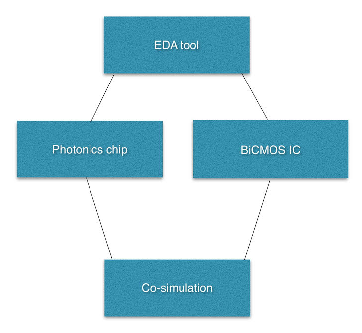
Benetti also highlights the progress being made with silicon photonics circuit design tools.
STMicro's test circuits currently in the fab have been developed using electronic design automation (EDA) tools. "Already the first generation design kit is rather complete - not only the physical design tools for the optics and electronics but also the ability to simulate the system [the two together] with the EDA tools," says Benetti.
But challenges remain.
One is the ability to get light in and out of the chip in an industrial way. "Coupling the light in the fibre attachment - these are processes that still have a high degree of improvement," says Benetti. "The process of the fibre attachment and the packaging is something we are working a lot on. We have today at a very good stage of speed and precision in the placement of the fibres but there is still much we can do."