Nokia's 4.8-terabit FP5 packet-processing chipset

Part 1: IP routing: Nokia’s latest FP5 and router platforms
Nokia has unveiled its latest packet-processing silicon that will be the mainstay of its IP router platforms for years to come.
The FP5 chipset is rated at 4.8 terabits-per-second (Tbps), a twelvefold improvement in Nokia’s packet-processing silicon performance in a decade. (See chart.)

Communications service provider (CSP) BT says Nokia’s 7750 router platforms equipped with the FP5 chipset will deliver every use case it needs for its Multi Service Edge; from core routing, MPLS-VPN, broadband network gateways (BNG), to mobile backhaul and Ethernet.
The FP5 announcement comes four years after Nokia unveiled its existing flagship router chipset, the FP4. The FP4 was announced as a 2.4Tbps chipset but Nokia upgraded its packet-processing rating to 3Tbps.
“We announced what we knew but then, through subsequent development and testing, the performance ended up at 3Tbps,” says Heidi Adams, head of IP and optical networks marketing at Nokia.
The FP5 may also exceed its initial 4.8Tbps rating.
Nokia will use the FP5 to upgrade its existing platforms and power new router products; it will not license the chipset nor will it offer it for use in open router platforms.
Nokia’s chipset evolution
At the heart of Nokia’s router silicon is a 2D array of packet processing cores.
The FP3, announced in 2011 by Alcatel-Lucent (acquired by Nokia in 2016), used 288 packet processing cores arranged in a 32×9 array. Each row of cores acted as a packet-processing pipeline that could be partitioned to perform independent tasks. The array’s columns performed table look-ups and each column could be assigned several tasks.
Nokia didn’t detail how the FP4 upgraded the array of cores. But the performance enhancement was significant; the FP4 delivers a 7.5x improvement in packet processing performance compared to the FP3.
The 16nm CMOS FP4 chipset includes a traffic manager (q-chip), packet processor (p-chip), the t-chip that interfaces to the router fabric, and what was then a new chip, the e-chip.
The e-chip acts as a media access controller (MAC) that parcels data from the router’s client-side pluggable optical modules for the p-chip.
Nokia even designed memory for the FP4 whereby instructions can be implemented during memory access and the memory can be allocated to perform different types of look-up and buffering, depending on requirements.
To maximise the memory’s performance, Nokia used advanced packaging for the FP4’s p-chip and q-chip. The resulting 2.5D-packaged p-chip comprises the packet processor die and stacks of memory. The q-chip is also a multi-chip module containing RISC processors and buffering memory.
The FP4 uses 56Gbps PAM-4 serialiser-deserialiser (serdes) interfaces, technology that Nokia secured from Broadcom.
FP5’s features
The FP5 builds on the major architectural upgrade undertaken with the FP4.
Using a 7nm CMOS process technology, Nokia’s FP5 designers have combined on-chip what were two separate FP4 chips: the packet processor (p-chip) and traffic manager (q-chip).
The FP5 chipset consumes a quarter of the power of the FP4 in terms of watts-per-gigabit (0.1W/Gig for the FP5 compared to the FP4’s 0.4W/Gig).
Consolidating two chips into one accounts for part of the power savings. Using 112Gbps serdes and a more advanced CMOS process are other factors.
Nokia has also added encryption hardware blocks to the chip’s ports. The hardware blocks implement the MACsec algorithm and can also encrypt layer 2.5 and layer 3 traffic.
The chipset can handle packet flows as large as 1.6 terabits. “We don’t have any physical interfaces that support flows at that rate,” says Adams. “It’s an indicator that the chipset is ready for much more.”
The e-chip, which Nokia describes as a tremendously important device, has also been upgraded. As well as the MAC function, it acts as an early-stage packet processor, performing pre-processing and pre-classification tasks on the traffic.
The e-chip also performs pre-buffering for the packer processor. Using multiple such devices allows the line card to expand the forwarding limit of the FP5’s packet processor. This enables Nokia’s routers to perform what it calls intelligent aggregation (IA). “We can bring in more traffic, increase the number of ingress ports even if those ports start to get fully loaded, because of the chipset architecture being fully buffered,” says Adams. “The result is a 30 per cent uplift in the stated capacity numbers.”
The FP5 chipset has been taped out and the silicon is being tested in Nokia’s lab.
Router platforms
IP core routers are tasked with moving large amounts of IP traffic across a network backbone. IP edge routers, in contrast, typically aggregate a variety of services such as mobile transport, residential traffic or act as gateways.
The platforms that will use the FP5 are classified by Nokia as edge routers. “The boundaries have blurred,” says Adams. “It is more important to look at how applications are deployed and what the requirements are.”
The platforms using the FP5 are the existing 7750 SR-14s and 7750-SR7s routers that were announced with the launch of the FP4.
These chassis were designed to accommodate Nokia’s current and next-generation router cards. “This allows operators to retain the same chassis and support a mix of FP4 and FP5 cards, growing into them gradually,” says Adams.
Nokia has announced three other platforms: two mid-range platforms, the 7750 SR2-se and the 7750 SR1-se, and the 7750 SR-1 that will be available in six variants. “They [the SR-1 boxes] are going to be available in a range of configurations and different port speeds,” says Adams.
Platforms using the FP5 chipset will ship in the first half of 2022, starting with the SR-1.
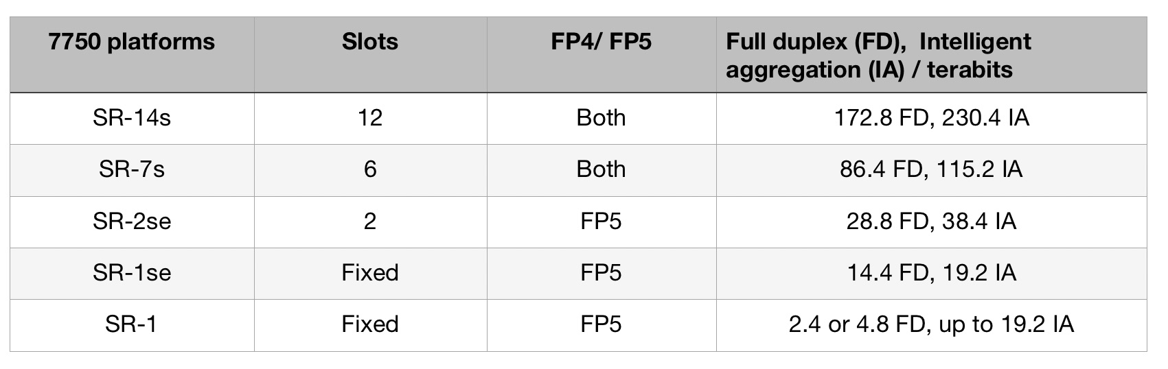
Nokia also announced an FP5 expandable media adaptor (XMA) line card for the non-fixed platforms (the 7750 SR-14s/ SR-7s and SR-2se). The card supports 36 pluggable slots and with 400 Gigabit Ethernet (GbE) has a capacity of 14.4Tbps full-duplex or 19.2Tbps in intelligent aggregation mode.
The card will also support 400ZR and ZR+ coherent modules and is ready for 800GbE pluggables that will double the card’s capacity ratings.
Nokia says the FP5 improves the throughput of the XMA card by a factor of three: Nokia’s 4.8Tbps XMA (12Tbps IA) uses four FP4 chipsets while the latest 14.4Tbps (19.2Tbps IA) XMA uses six FP5 chipsets.
Custom silicon versus disaggregated designs
Nokia says the benefits of having its own chipset justify the intellectual effort and development expense, even when advanced merchant silicon is available and certain CSPs are embracing open disaggregated routers.
“We feel there is a need in the industry for platforms based on this kind of technology,” says Adams.
What is important is the total cost of ownership and that Nokia’s systems are deployed in critical networks where resiliency, reliability, the feature set and network security are all critical, says Adams.
Nokia also points to the progress it has made since the launch of the FP4. “We have secured 350 projects, two-thirds of which were new footprints or competitive displacements,” says Adams. Nokia’s IP revenues in 2020 were $3.2 billion.
That said, Nokia also partners with merchant silicon vendors: the 7250 IXR interconnect router uses merchant silicon, for example.
“If I look at disaggregation, absolutely, it is an interesting area,” says Adams. “But I think it is very early days.”
Neil McRae, managing director and chief architect at BT, says that while some operators are looking at disaggregated software and hardware, BT doesn’t believe this is necessarily the best solution in terms of performance, reliability or cost.
“Increasingly, the ratio of capital investment in core networking is moving towards optical transceivers than router silicon,” says McRae. “But to get the most out of the network and the router, using custom silicon for the most demanding cases still delivers the best outcomes.
“In our live network but also in our testing, the integrated solution is more reliable, easier to operate and a significant improvement from a total cost of ownership point of view,” says McRae.
BT says it will be able to scale interfaces on the 7750 from 1-400Gbs using the FP5 and Nokia’s SR-OS routing networking software.
BT also highlights the importance of reliability under demand, pointing out how the CSP’s traffic has doubled during the pandemic without impacting its customers.
“Nokia’s understanding of how the underlying silicon is going to react in different situations gives them a significant advantage in building the software on top that performs in challenging situations,” says McRae.
Chip Strategy
Nokia says that were it to sell its FP5 silicon as a standalone product, it would enter a very different design environment.
“You are designing to the requirements of multiple customers versus designing for your systems,” says Adams.
Nokia’s belief is that there is strong demand for platforms designed to purpose.
“We are staying true to that strategy,” says Adams.

The era of cloud-scale routeing
 Nokia's FP4 p-chip. The multi-chip module shows five packages: the p-chip die surrounded by four memory stacks. Each stack has five memory die. The p-chip and memory stacks are interconnected using an interposer.
 - Nokia has unveiled the FP4, a 2.4 terabit-per-second network processor that has 6x the throughput of its existing FP3.
- The FP4 is a four-IC chipset implemented using 16nm CMOS FinFET technology. Two of the four devices in the chipset are multi-chip modules.
- The FP4 uses 56 gigabit-per-second serial-deserialiser (serdes) technology from Broadcom, implemented using PAM-4 modulation. It also supports terabit flows.
- Nokia announced IP edge and core router platforms that will use the FP4, the largest configuration being a 0.58 petabit switching capacity router.
Much can happen in an internet minute. In that time, 4.1 million YouTube videos are viewed, compared to 2.8 million views a minute only last year. Meanwhile, new internet uses continue to emerge. Take voice-activated devices, for example. Amazon ships 50 of its Echo devices every minute, almost one a second.
Given all that happens each minute, predicting where the internet will be in a decade’s time is challenging. But that is the task Alcatel-Lucent’s (now Nokia’s) chip designers set themselves in 2011 after the launch of its FP3 network processor chipset that powers its IP-router platforms.
Six years on and its successor - the FP4 - has just been announced. The FP4 is the industry’s first multi-terabit network processor that will be the mainstay of Nokia’s IP router platforms for years to come.
Cloud-scale routing
At the FP4’s launch, Nokia’s CEO, Rajeev Suri, discussed the ‘next chapter’ of the internet that includes smart cities, new higher-definition video formats and the growing number of connected devices.
IP traffic is growing at a compound annual growth rate (CAGR) of 25 percent through to 2022, according to Nokia Bell Labs, while peak data rates are growing at a 39 percent CAGR. Nokia Bell Labs also forecasts that the number of connected devices will grow from 12 billion this year to 100 billion by 2025.
Basil Alwan, Nokia’s president of IP and optical networks, said the internet has entered the era of cloud-scale routeing. When delivering a cloud service, rarely is the request fulfilled by one data centre. Rather, several data centres are involved in fulfilling the tasks. “One transaction to the cloud is multiplied,” said Alwan.
IP traffic is also becoming more dynamic, while the Internet of Things presents a massive security challenge.
Alwan also mentioned how internet content providers have much greater visibility into their traffic whereas the telcos’ view of what flows in their networks is limited. Hence their interest in analytics to understand and manage their networks better.
These are the trends that influenced the design of the FP4.
We put a big emphasis on making sure we had a high degree of telemetry coming out at the chip level
FP4 goals
Telemetry, the sending of measurement data for monitoring purposes, and network security were two key design goals for the FP4.
 Steve Vogelsang“We put a big emphasis on making sure we had a high degree of telemetry coming out at the chip level,” said Steve Vogelsang, CTO for Nokia's IP and optical business.
Tasks include counters, collecting statistics and packet copying. “This is to make sure we have the instrumentation coming off these systems that we can use to drive the [network] analytics platform,” said Vogelsang.
Being able to see the applications flowing in the network benefits security. Distributed Denial-of-Service (DDoS) attacks are handled by diverting traffic to a ‘scrubbing centre’ where sophisticated equipment separates legitimate IP packets from attack traffic that needs scrubbing.
The FP4 supports the deeper inspection of packets. “Once we identify a threat, we can scrub that traffic directly in the network,” said Vogelsang. Nokia claims that that the FP4 can deal with over 90 percent of the traffic that would normally go to a scrubbing centre.
Chipset architecture
Nokia’s current FP3 network processor chipset comprises three devices: the p-chip network processor, the q-chip traffic manager and the t-chip fabric interface device.
The p-chip network processor inspects packets and performs table look-ups using fast-access memory to determine where packets should be forwarded. The q-chip is the traffic manager that oversees the packet flows and decides how packets should be dealt with, especially when congestion occurs. The third FP3 chip is the t-chip that interfaces to the router fabric.
The FP4 retains the three chips and adds a fourth: the e-chip - a media access controller (MAC) that parcels data from the router’s client-side pluggable optical modules for the p-chip. However, while the FP4 retains the same nomenclature for the chips as the FP3, the CMOS process, chip architecture and packaging used to implement the FP4 are significantly more advanced.
The FP4 can deal with over 90 percent of the traffic that would normally go to a scrubbing centre
Nokia is not providing much detail regarding FP4 chipset's architecture, unlike the launch of the FP3. “We wanted to focus on the re-architecture we have gone through,” said Vogelsang. But looking at the FP3 design, insight can be gained as to how the FP4 has likely changed.
The FP3’s p-chip uses 288 programmable cores. Each programmable core can process two instructions each clock cycle and is clocked at 1GHz.
The 288 cores are arranged as a 32-row-by-9-column array. Each row of cores can be viewed as a packet-processing pipeline. A row pipeline can also be segmented to perform independent tasks. The array’s columns are associated with table look-ups. The resulting FP3 p-chip is a 400-gigabit network processor.
Vogelsang said there is limited scope to increase the clock speed of the FP4 p-chip beyond 1GHz. Accordingly, the bulk of the FP4’s sixfold throughput improvement is the result of a combination of programmable core enhancements, possible a larger core array and, most importantly, system improvements. In particular, the memory architecture is now packaged within the p-chip for fast look-ups, while the chipset’s input-output lanes have been boosted from 10 gigabits-per-second (Gbps) to 50Gbps.
Nokia has sought to reuse as much of the existing microcode to program the cores for the FP4 p-chip but has added new instructions to take advantage of changes in the pipeline.
Software compatibility already exists at the router operating system level. The same SROS router operating system runs on Nokia’s network processors, merchant hardware from the like of Broadcom and on x86 instruction-set microprocessors in servers using virtualisation technology.
Such compatibility is achieved using a hardware abstraction layer that sits between the operating system and the underlying hardware. “The majority of the software we write has no idea what the underlying hardware is,” said Vogelsang.
Nokia has a small team of software engineers focussed on the FP4’s microcode changes but, due to the hardware abstraction layer, such changes are transparent to the main software developers.
The FP3’s traffic manager, the q-chip, comprises four reduced instruction set computer (RISC) cores clocked at 900MHz. This too has been scaled up for the FP4 but Nokia has not given details.
The t-chip interfaces to the switch fabric that sits on a separate card. In previous generations of router products, a mid-plane is used, said Nokia. This has been scrapped with the new router products being announced. Instead, the switch cards are held horizontally in the chassis and the line cards are vertical. “A bunch of metal guides are used to guide the two cards and they directly connect to each other,” said Vogelsang. “The t-chips are what interface to these connectors inside the system.”
The MAC e-chip interfaces to the line card’s pluggable modules and support up to a terabit flow. Indeed, the MAC will support integer multiples of 100 Gigabit Ethernet from 100 gigabit to 1 terabit. Nokia has a pre-standard implementation of FlexMAC that allows it to combine lanes across multiple transceivers into a single interface.
Nokia will have line cards that support 24 or 36 QSFP-DD pluggable modules, with each module able to support 400 Gigabit Ethernet.
The FP4 is also twice as power efficient, consuming 4 gigabit/W.
We wanted to make sure we used a high-volume chip-packaging technology that was being driven by other industries and we found that in the gaming industry
Design choices
One significance difference between the two network processor generations is the CMOS process used. Nokia skipped 28nm and 22nm CMOS nodes to go from 40nm CMOS for the FP3 to 16nm FinFET for the FP4. “We looked at that and we did not see all the technologies we would need coming together to get the step-function in performance that we wanted,” said Vogelsang.
Nokia also designed its own memory for the FP4.
“A challenge we face with each generation of network processor is finding memories and memory suppliers that can offer the performance we need,” said Vogelsang. The memory Nokia designed is described as intelligent: instructions can effectively be implemented during memory access and the memory can be allocated to do different types of look-up and buffering, depending on requirements.
Another key area associated with maximising the performance of the memory is the packaging. Nokia has adopted multi-chip module technology for the p-chip and the q-chip.
“We wanted to make sure we used a high-volume chip-packaging technology that was being driven by other industries and we found that in the gaming industry,” said Vogelsang, pointing out that the graphics processing unit (GPU) has similar requirements to those of a network processor. GPUs are highly memory intensive while manipulating bits on a screen is similar to manipulating headers and packets.
The resulting 2.5D packaged p-chip comprises the packet processor die and stacks of memory. Each memory stack comprises 5 memory die. All sit on an interposer substrate - itself a die that is used for dense interconnect of devices. The resulting FP4 p-chip is thus a 22-die multi-chip module.
“Our memory stacks are connected at the die edges and do not use through-silicon vias,” said Vogelsang. “Hence it is technically a 2.5D package [rather than 3D].”
The q-chip is also implemented as a multi-chip module containing RISC processors and buffering memory, whereas the router fabric t-chip and MAC e-chip are single-die ICs.
The FP4’s more advanced CMOS process also enables significantly faster interfaces. The FP4 uses PAM-4 modulation to implement 56Gbps interfaces. “You really need to run those bit rates much much higher to get the traffic into and out of the chip,” said Vogelsang.
Nokia says it is using embedded serialiser-deserialiser interface technology from Broadcom.
Next-gen routers
Nokia has also detailed the IP edge and core routers that will use the FP4 network processor.
The 7750 Service Router (SR-s) edge router family will support up to 144 terabits in a single shelf. This highest capacity configuration is the 7750 SR-14. It is a 24-rack-unit-plus-the-power-supply high chassis and supports a dozen line cards, each 12Tbps when using 100-gigabit modules, or 24x400GbE when using QSFP-DD modules.
Another new platform is the huge 7950 Extensible Routing System (XRS-XC) IP core router which can be scaled to 576 terabits - over half a petabit - when used in a six-chassis configuration. Combining the six chassis does not make require the use of front-panel client-side interfaces. Instead, dedicated interfaces are used with active optical cables to interlink the chassis.
The first router products will be shipped to customers at the year end with general availability expected from the first quarter of 2018.
COBO: specification work nearing completion
The Consortium for On-board Optics (COBO) is on target to complete its specifications work by the year end. The work will then enter a final approval stage that will take up to a further three months.

On-board optics, also known as mid-board or embedded optics, have been available for years but vendors have so far had to use custom products. The goal of COBO, first announced in March 2015 and backed by such companies as Microsoft, Cisco Systems, Finisar and Intel, is to develop a technology roadmap and common specifications for on-board optics to ensure interoperability.
Brad Booth (pictured), the chair of COBO and principal architect for Microsoft’s Azure Global Networking Services, says that bringing optics inside systems raises a different set of issues compared to pluggable optical modules used on the front panel of equipment. “If you have a requirement for 32 ports on a faceplate, you know mechanically what you can build,” says Booth.
With on-board optics, the focus is less about size considerations and more about the optical design itself and what is needed to make it work. There is also more scope to future-proof the design, something that can not be done so much with pluggable optics, says Booth.
COBO is working on a 400-gigabit optical module based on the 8-by–50 gigabit interface. The focus in recent months has been on defining the electrical connector that will be needed. The group has narrowed down the choice of candidates to two and the final selection will be based on the connector's signal integrity performance and manufacturability. Also being addressed is how two such modules could be placed side-by-side to create an 800-gigabit (16-by–50 gigabit) design.
COBO’s 400-gigabit on-board optics will support multi-mode and single-mode fibre variants. “When we do a comparison with what the pluggable people are pushing, there are a lot of pluggables that won’t be able to handle the power envelope,” says Booth.
There is no revolutionary change that goes on with technology, it all has to be evolutionary
On-board optics differs from a pluggable module in that the optics and electronics are not confined within a mechanical enclosure and therefore power dissipation is less of an design issue. But by supporting different fibre requirements and reaches new design issues arise. For example, when building a 16-by–50 gigabit design, the footprint is doubled and COBO is looking to eliminate the gap between the two such that a module can be plugged in that is either 8- or 16-lanes wide.
COBO is also being approached about supporting other requirements such as coherent optics for long-distance transmission. A Coherent Working Group has been formed and will meet for the first time in December in Santa Barbara, California. Using on-board optics for coherent avoids the power constraint issues associated with using a caged pluggable module.
On-board optics versus co-packaging
On-board optics is seen as the next step in the evolution of optics as it moves from the faceplate onto the board, closer to the ASIC. There is only so many modules that can fit on a faceplate. The power consumption also raises as the data rate of a pluggable modules increases, as does the power associated with driving faster electrical traces across the board.
Using on-board optics shortens the trace lengths by placing the optics closer to the chip. The board input-output capacity that can be supported also increases as it is fibres not pluggable optics that reside on the front panel. Ultimately, however, designers are already exploring the combining of optics and the chip using a system-in-package design, also known as 2.5D or 3D chip packaging.
Booth says discussions have already taken place between COBO members about co-packaged optics. But he does not expect system vendors to stay with pluggable optics and migrate directly to co-packaging thereby ignoring the on-board optics stage.
“There is no revolutionary change that goes on with technology, it all has to be evolutionary,” says Booth, who sees on-board optics as the next needed transition after pluggables. “You have to have some pathway to learn and discover, and figure out the pain points,” he says. “We are going to learn a lot when we start the deployment of COBO-based modules.”
Booth also sees on-board optics as the next step in terms of flexibility.
When pluggable modules were first introduced they were promoted as allowing switch vendors to support different fibre and copper interfaces on their platforms. The requirements of the cloud providers has changed that broad thinking, he says: “We don’t need that same level of flexibility but there is still a need for suporting different styles of optical interfaces on a switch.”
There are not a lot of other modules that can do 600 gigabit but guess what? COBO can
For example, one data centre operator may favour a parallel fibre solution based on the 100-gigabit PSM4 module while another may want a 100-gigabit wavelength-division multiplexing (WDM) solution and use the CWDM4 module. “This [parallel lane versus WDM] is something embedded optics can cater for,” says Booth.
Moving to a co-packaged design offers no such flexibility. What can a data centre manager do when deciding to change from parallel single-mode optics to wavelength-division multiplexing when the optics is already co-packaged with the chip? “Also how do I deal with an optics failure? Do I have to replace the whole switch silicon?” says Booth. We may be getting to the point where we can embed optics with silicon but what is needed is a lot more work, a lot more consideration and a lot more time, says Booth.
Status
COBO members are busy working on the 400-gigabit embedded module, and by extension the 800-gigabit design. There is also ongoing work as to how to support technologies such as the OIF’s FlexEthernet. Coherent designs will soon support rates such as 600-gigabit using a symbol rate of 64 gigabaud and advanced modulation. “There are not a lot of other modules that can do 600 gigabits but guess what? COBO can,” says Booth.
The good thing is that whether it is coherent, Ethernet or other technologies, all the members are sitting in the same room, says Booth: “It doesn’t matter which market gets there first, we are going to have to figure it out.”
Story updated on October 27th regarding the connector selection and the Coherent Working Group.
The making of integrated optics
A US initiative is bringing together leading companies with top academics and universities to create a manufacturing infrastructure for the widespread adoption of integrated photonics.
The US sees integrated photonics as a strategic technology and has set up the American Institute for Manufacturing Integrated Photonics - AIM Photonics - to advance the technology and make it available to a wider community of companies. AIM Photonics, with $610 million of public and private funding, is a five-year initiative ending in 2020. AIM’s long-term goal is to be self-sustaining.
 Doug Coolbaugh
“Right now the infrastructure is focussed on electronics and CMOS but photonics is going to be the future,” says Doug Coolbaugh, chief operations officer at AIM Photonics. “There is no other way to do it [very high bandwidth] except using light for ultra fast communications.”
Technologies start at universities and in the labs of companies with large R&D budgets. IBM and Intel, for example, have been developing silicon photonics for over a decade and the technology is ready for deployment. However, the intellectual property developed remains with such companies.
“AIM is not only creating the manufacturing infrastructure for integrated photonics but also ideas and intellectual property that can be used by companies for new products,” says Coolbaugh.
All the elements are being addressed so that small to medium businesses and entrepreneurial ventures can use integrated photonics for their products; companies too small to develop the technology themselves. “That will accelerate the silicon photonics ecosystem and allow new products to come out much faster than it would normally take,” says Coolbaugh.
Manufacturing
Silicon photonics luminary, Lionel Kimerling, professor of materials science and engineering at MIT, and an active member of AIM Photonics, views its focus on manufacturing as an important development.
The discipline of manufacturing is something that the chip industry has mastered through designing process integration, selecting materials and all the qualification standards used to meet system requirements, he says, but is less developed in the photonics industry.
AIM is making available a chip fabrication plant to interested companies. SUNY Polytechnic Institute has been working with MIT for the last six years to develop a 300mm-wafer silicon photonics line at its Albany site. The fab offers a multi-project wafer service whereby several designs can be made on a single wafer, allowing costs to be shared among companies.
AIM is not only creating the manufacturing infrastructure for integrated photonics but also ideas and intellectual property that can be used by companies for new products
A design kit is also being developed featuring key building blocks needed to make an integrated photonics circuit. AIM is working with leading semiconductor industry design automation companies Cadence, Synopsys and Mentor Graphics to provide the software tool environment for designers to develop circuits. “This design environment is compatible with the silicon photonics process here in our fab,” says Coolbaugh.
A packaging and prototyping facility located in Rochester, New York is also being set up. “Photonics packaging is relatively new and certain aspects have not been developed that much,” says Coolbaugh.
Another issue is developing skilled engineers and technicians able to design and manufacture integrated photonics circuits. Whereas electronic chip designers typically have a first degree, photonics engineers tend to have a doctorate because of the deep understanding needed. “This is one of the things we find we are lacking significantly,” says Coolbaugh. “There are just not enough skilled people in the industry to fulfil these needs.”
Professor Kimerling says he is spending much of his time putting together educational material to help attract individuals to pursue a career in silicon photonics. Much of the technology is in place, he says, what is required is to make it accessible to people. “I don’t have 40 more years in the industry, but I could influence the next 40 years by creating these instructional materials and career paths, and getting roadmap consensus that can drive the industry,” says Kimerling.
AIM is also working with universities and companies to develop technology and intellectual property alongside the manufacturing centres. Four research areas have been chosen, covering datacom, analogue RF for telecom involving Infinera, sensors and phased arrays. These are areas where AIM sees products emerging in volume in the next five years.
Keren Bergman, whose work focusses on the intersection of photonics and computing systems, mentions how AIM Photonics has already benefited her research group through much closer interactions with companies in the area of datacom. “It has had a big impact on our work,” says Bergman, professor and director at the Lightwave Research Laboratory at Columbia University.
Each year AIM will review and add new research topics. “There are new ideas, new materials and new manufacturing processes that will be developed,” says Coolbaugh. He cites the use of silicon photonics to drive robots as an emerging application area.
Status
AIM expects the entire manufacturing infrastructure to be in place in the next couple of years.
“Right now it is only the photonics design part but we will also be putting in interposers for packaged designs," says Coolbaugh. Interposers are a key technology that allows the co-packaging of chip dice, an approach known as system-in-package or 2.5D packaging.
AIM expects to offer multi-project wafers with interposers and system-in-package by 2017, with the ability to add CMOS dice in 2018. AIM is also developing a test, assembly and packaging facility which it expects to be available by 2018. “Testing is a really critical component of this entire infrastructure,” says Coolbaugh.
The goal is to develop new ways of fast-testing photonics on wafers, while there will be the high-speed testing of circuits at Rochester. “What we design has got to work in the fab, the fab has got to test well and then what we package has to be consistent with what we deliver to the packaging house,” says Coolbaugh. “The entire flow has to integrate exactly.”
A start-up or small company wanting to make a product can already use the design kit - which continues to evolve - and benefit from AIM’s multi-project wafer service. Then there will be the Rochester packaging and prototyping site. Low volumes can be made at the Albany fab while AIM will pass higher-volume manufacturing requests to leading chip fabrication players such as GlobalFoundries.
Companies can take a concept, develop their own product and have their own business. “We provide the entire chain for the infrastructure,“ says Coolbaugh. ”Right now, this is only available to large companies.”
If all goes to plan, what impact will AIM have on integrated optics and silicon photonics in particular? “It will be a worldwide impact,” says Coolbaugh. “Just because we want to create the infrastructure in the US doesn’t mean we are limiting our customers to the US.”
Further information
For AIM Photonics presentations, click here
The text is based on an article that first appeared in Optical Connections magazine