
Rockley Photonics eyes multiple markets
Andrew Rickman, founder and CEO of silicon photonics start-up, Rockley Photonics, discusses the new joint venture with Hengtong Optic-Electric, the benefits of the company’s micron-wide optical waveguides and why the timing is right for silicon photonics.
 Andrew Rickman
The joint venture between Rockley Photonics and Chinese firm Hengtong Optic-Electric is the first announced example of Rockley’s business branching out.
The start-up’s focus has been to apply its silicon photonics know-how to data-centre applications. In particular, Rockley has developed an Opto-ASIC package that combines optical transceiver technology with its own switch chip design. Now it is using the transceiver technology for its joint venture.
“It was logical for us to carve out the pieces generated for the Opto-ASIC and additionally commercialise them in a standard transceiver format,” says Andrew Rickman, Rockley’s CEO. “That is what the joint venture is all about.”
Rockley is not stopping there. Rickman describes the start-up as a platform business, building silicon photonics and electronics chipsets for particular applications including markets other than telecom and datacom.
Joint venture
Hengtong and Rockley have set up the $42 million joint venture to make and sell optical transceivers.
Known for its optical fibre cables, Hengtong is also a maker of optical transceivers and owns 75.1 percent of the new joint venture. Rockley gains the remaining 24.9 percent share in return for giving Hengtong its 100-gigabit QSFP transceiver designs. The joint venture also becomes a customer of Rockley’s, buying its silicon photonics and electronics chips to make the QSFP modules.
“Hengtong is one of the world’s largest optical fibre cable manufacturers, is listed on the Shanghai stock market, and sells extensively in China and elsewhere into the data centre market,” says Rickman. “It is a great conduit, a great sales channel into these customers.”
The joint venture will make three 100-gigabit QSFP-based products: a PSM4 and a CWDM4 pluggable module and an active optical cable. Rickman expects the joint venture to make other module designs and points out that Rockley participates in the IEEE standards work for 400 gigabits and is one of the co-founders of the 400-gigabit CWDM8 MSA.
Rockley cites several reasons why the deal with Hengtong makes sense. First, a large part of the bill of materials used for active optical cables is the fibre itself, something which the vertically integrated Hengtong can provide.
China also has a ‘Made in China 2025’ initiative that encourages buying home-made optical modules. Teaming with Hengtong means Rockley can sell to the Chinese telecom operators and internet content players.
In addition, Hengtong is already doing substantial business with all of the global data centres as a cable, patch panel and connector supplier, says Rickman:“So it is an immediate sales channel into these companies without having to break into these businesses as a qualified supplier afresh.”
A huge amount of learning happened and then what Rockley represented was the opportunity to start all over again with a clean sheet of paper but with all that experience
Bigger is Best?
At the recent SPIE Photonics West conference held in San Francisco, Rickman gave a presentation entitled Silicon Photonics: Bigger is Better. His talk outlined the advantages of Rockley’s use of three-micron-wide optical waveguides, bucking the industry trend of using relatively advanced CMOS processes to make silicon photonics components.
Rickman describes as seductive the idea of using 45nm CMOS for optical waveguides.“These things exist and work but people are thinking of them in the same physics that have driven microelectronics,” he says. Moving to ever-smaller feature sizes may have driven Moore’s Law but using waveguide dimensions that are smaller than the wavelength of light makes things trickier.
To make his point, he plots the effective index of a waveguide against its size in microns. The effective index is a unitless measure - a ratio of a phase delay in a unit length of a waveguide relative to the phase delay in a vacuum. “Once you get below one micron, you get a waveguide that is highly polarisation-dependent and just a small variation in the size of the waveguide has a huge variation in the effective index,” says Rickman.
Such variations translate to inaccuracies in the operating wavelength. This impacts the accuracy of circuits, for example, arrayed-waveguide gratings built using waveguides to multiplex and demultiplex light for wavelength-division multiplexing (WDM).
“Above one micron is where you want to operate, where you can manufacture with a few percent variation in the width and height of a waveguide,” says Rickman.“But the minute you go below one micron, in order to hit the wavelength registration that you need for WDM, you have got to control the [waveguide’s] film thickness and line thickness to fractions of a percent.” A level of accuracy that the semiconductor industry cannot match, he says.
A 100GHz WDM channel equates to 0.8nm when expressed using a wavelength scale. “In our technology, you can easily get a wavelength registration on a WDM grid of less than 0.1nm,” says Rickman. “Exactly the same manufacturing technology applied to smaller waveguides is 25 times worse - the variation is 2.5nm.”
Moreover, WDM technology is becoming increasingly important in the data centre. The 100-gigabit PSM4 uses a single wavelength, the CWDM4 uses four, while the newer CWDM8 MSA for 400 gigabit uses eight wavelengths. “In telecom, 90-plus wavelengths can be used; the same thing will come to pass in the years to come in data centre devices,” he says.
Rockley also claims it has a compact modulator that is 50 times smaller than competing modulators despite them being implemented using nanometer feature sizes.
We set out to generate a platform that would be pervasive across communications, new forms of advanced computing, optical signal processing and a whole range of sensor applications
Opto-ASIC reference design
Rockley’s first platform technology example is its Opto-ASIC reference design. The design integrates silicon photonics-based transceivers with an in-house 2 billion transistor switch chip all in one package. Rockley demonstrated the technology at OFC 2017.
“If you look around, this is something the industry says is going to happen but there isn't a single practical instantiation of it,” says Rickman who points out that, like the semiconductor industry, very often a reference design needs to be built to demonstrate the technology to customers.“So we built a complete reference design - it is called Topanga - an optical-packaged switch solution,” he says.
Despite developing a terabyte-class packet processor, Rockley does not intend to compete with the established switch-chip players. The investment needed to produce a leading edge device and remain relevant is simply too great, he says.
Rockley has demonstrated its in-package design to relevant companies. “It is going very well but nothing we can say publicly,” says Rickman.
New Markets
Rockley is also pursuing opportunities beyond telecom and datacom.
“We set out to generate a platform that would be pervasive across communications, new forms of advanced computing, optical signal processing and a whole range of sensor applications,” says Rickman.
Using silicon photonics for sensors is generating a lot of interest. “We see these markets starting to emerge and they are larger than the data centre and communications markets,” he says. “A lot of these things are not in the public domain so it is very difficult to report on.”
Moreover, the company’s believes its technology gives it an advantage for such applications. “When we look across the other application areas, we don’t see the small waveguide platforms being able to compete,” says Rickman. Such applications can use relatively high power levels that exceed what the smaller waveguides can handle.
Rockley is sequencing the markets it will address. “We’ve chosen an approach where we have looked at the best match of the platform to the best opportunities and put them in an order that makes sense,” says Rickman.
Rockley Photonics represent Rickman’s third effort to bring silicon photonics to the marketplace.Bookham Technology, the first company he founded, build different prototypes in several different areas but the market wasn't ready. In 2005 he joined start-up Kotura as a board member. “A huge amount of learning happened and then what Rockley represented was the opportunity to start all over again with a clean sheet of paper but with all that experience,” says Rickman.
Back in 2013, Rockley saw certain opportunities for its platform approach and what has happened since is that their maturity and relevance has increased dramatically.
“Like all things it is always down to timing,” says Rickman. “The market is vastly bigger and much more ready than it was in the Bookham days.”
ECOC '15 Reflections: Part 2
Martin Zirngibl, head of network enabling components and technologies at Bell Labs.
Silicon Photonics is seeming to gain traction, but traditional component suppliers are still betting on indium phosphide.
There are many new start-ups in silicon photonics, most seem to be going after the 100 gigabit QSFP28 market. However, silicon photonics still needs a ubiquitous high-volume application for the foundry model to be sustainable.
There is a battle between 4x25 Gig CWDM and 100 Gig PAM-4 56 gigabaud, with most people believing that 400 Gig PAM-4 or discrete multi-tone with 100 Gig per lambda will win.
Will coherent make it into black and white applications - up to 80 km - or is there a role for a low-cost wavelength-division multiplexing (WDM) system with direct detection?
One highlight at ECOC was the 3D integrated 100 Gig silicon photonics by Kaiam.
In coherent, the analogue coherent optics (ACO) model seems to be winning over the digital coherent one, and people are now talking about 400 Gig single carrier for metro and data centre interconnect applications.
As for what I’ll track in the coming year: will coherent make it into black and white applications - up to 80 km - or is there a role for a low-cost wavelength-division multiplexing (WDM) system with direct detection?
Yukiharu Fuse, director, marketing department at Fujitsu Optical Components
There were no real surprises as such at ECOC this year. The products and demonstrations on show were within expectations but perhaps were more realistic than last year’s show.
Most of the optical component suppliers demonstrated support to meet the increasing demand of data centres for optical interfaces.
The CFP2 Analogue Coherent Optics (CFP2-ACO) form factor’s ability to support multiple modulation formats configurable by the user makes it a popular choice for data centre interconnect applications. In particular, by supporting 16-QAM, the CFP2-ACO can double the link capacity using the same optics.
Lithium niobate and indium-phosphide modulators will continue to be needed for coherent optical transmission for years to come
Recent developments in indium phosphide designs has helped realise the compact packaging needed to fit within the CFP2 form factor.
I saw the level of integration and optical engine configurations within the CFP2-ACO differ from vendor to vendor. I’m interested to see which approach ends up being the most economical once volume production starts.
Oclaro introduced a high-bandwidth lithium niobate modulator for single wavelength 400 gigabit optical transmission. Lithium niobate continues to play an important role in enabling future higher baud rate applications with its excellent bandwidth performance. My belief is that both lithium niobate and indium-phosphide modulators will continue to be needed for coherent optical transmission for years to come.
Chris Cole, senior director, transceiver engineering at Finisar
ECOC technical sessions and exhibition used to be dominated by telecom and long haul transport technology. There is a shift to a much greater percentage focused on datacom and data centre technology.
What I learned at the show is that cost pressures are increasing
There were no major surprises at the show. It was interesting to see about half of the exhibition floor occupied by Chinese optics suppliers funded by several Chinese government entities like municipalities jump-starting industrial development.
What I learned at the show is that cost pressures are increasing.
New datacom optics technologies including optical packaging, thermal management, indium phosphide and silicon integration are all on the agenda to track in the coming year.
Verizon readies its metro for next-generation P-OTS
Verizon is preparing its metro network to carry significant amounts of 100 Gigabit traffic and has detailed its next-generation packet-optical transport system (P-OTS) requirements. The operator says technological advances in 100 Gig transmission and new P-OTS platforms - some yet to be announced - will help bring large scale 100 Gig deployments in the metro in the next year or so.
 Glenn Wellbrock
The operator says P-OTS will be used for its metro and regional networks for spans of 400-600km. "That is where we have very dense networks," says Glenn Wellbrock, director of optical transport network architecture and design at Verizon. "The amount of 100 Gig is going to be substantially higher than it was in long haul."
Verizon announced in April that it had selected Fujitsu and Coriant for a 100 Gig metro upgrade. The operator has already deployed Fujitsu's FlashWave 9500 and the Coriant 7100 (formerly Tellabs 7100) P-OTS platforms. "The announcement [in April] is to put 100 Gig channels in that embedded base," says Wellbrock.
The operator has 4,000 reconfigurable optical add/ drop multiplexers (ROADMs) across its metro networks worldwide and all support 100 Gig channels. But the networks are not tailored for high-speed transmission and hence the cost of 100 Gig remains high. For example, dispersion compensation fibre, and Erbium-doped fibre amplifiers (EDFA) rather than hybrid EDFA-Raman are used for the existing links. "It [the network] is not optimised for 100 Gig but will support it, and we are using [100 Gig] on an as-needed basis," says Wellbrock.
The metro platform will be similar to those used for Verizon's 100 Gig long-haul in that it will be coherent-based and use advanced, colourless, directionless, contentionless and flexible-grid ROADMs. "But all in a package that fits in the metro, with a much lower cost, better density and not such a long reach," says Wellbrock.
The amount of 100 Gig is going to be substantially higher than it was in long haul
One development that will reduce system cost is the advent of the CFP2-based line-side optical module; another is the emergence of third- or fourth-generation coherent DSP-ASICs. "We are getting to the point where we feel it is ready for the metro," says Wellbrock. "Can we get it to be cost-competitive? We feel that a lot of the platforms are coming along."
The latest P-OTS platforms feature enhanced packet capabilities, supporting carrier Ethernet, multi-protocol label switching - transport profile (MPLS-TP), and high-capacity packet and Optical Transport Network (OTN) switching. Recently announced P-OTS platforms suited to Verizon's metro request-for-proposal include Cisco Systems' Network Convergence System (NCS) 4000 and Coriant's mTera. Verizon says it expects other vendors to introduce platforms in the next year.
Verizon still has over 250,000 SONET elements in its network. Many are small and reside in the access network but SONET also exists in its metro and regional networks. The operator is keen to replace the legacy technology but with such a huge number of installed network elements, this will not happen overnight.
Verizon's strategy is to terminate the aggregated SONET traffic at its edge central offices so that it only has to deal with large Ethernet and OTN flows at the network node. "We plan to terminate the SONET, peel out the packets and send them in a packet-optimised fashion," says Wellbrock. In effect, SONET is to be stopped from an infrastructure point of view, he says, by converting the traffic for transport over OTN and Ethernet.
SDN and multi-layer optimisation
The P-OTS platform, with its integrated functionality spanning layer-0 to layer-2, will have a role in multi-layer optimisation. The goal of multi-layer optimisation is to transport services on the most suitable networking layer, typically the lowest, most economical layer possible. Software-defined networking (SDN) will be used to oversee such multi-layer optimisation.
However, P-OTS, unlike servers used in the data centre, are specialist rather than generic platforms. "Optical stuff is not generic hardware," says Wellbrock. Each P-OTS platform is vendor-proprietary. What can be done, he says, is to use 'domain controllers'. Each vendor's platform will have its own domain controller, above which will sit the SDN controller. Using this arrangement, the vendor's own portion of the network can be operated generically by an SDN controller, while benefitting from the particular attributes of each vendor's platform using the domain controller.
There is always frustration; we always want to move faster than things are coming about
Verizon's view is that there will be a hierarchy of domain and SDN controllers."We assume there are going to be multiple layers of abstraction for SDN," says Wellbrock. There will be no one, overriding controller with knowledge of all the networking layers: from layer-0 to layer-3. Even layer-0 - the optical layer - has become dynamic with the addition of colourless, directionless, contentionless and flexible-grid ROADM features, says Wellbrock.
Instead, as part of these abstraction layers, there will be one domain that will control all the transport, and another that is all-IP. Some software element above these controllers will then inform the optical and IP domains how best to implement service tasks such as interconnecting two data centres, for example. The transport controller will then inform each layer its particular task. "Now I want layer-0 to do that, and that is my Ciena box; I need layer-1 to do this and that happens to be a Cyan box; and we need MPLS transport to do this, and that could be Juniper," says Wellbrock, pointing out that in this example, three vendor-domains are involved, each with its own domain controller.
Is Verizon happy with the SDN progress being made by the P-OTS vendors?
"There is always frustration; we always want to move faster than things are coming about," says Wellbrock. "The issue, though, is that there is nothing I see that is a showstopper."
WDM and 100G: A Q&A with Infonetics' Andrew Schmitt
The WDM optical networking market grew 8 percent year-on-year, with spending on 100 Gigabit now accounting for a fifth of the WDM market. So claims the first quarter 2014 optical networking report from market research firm, Infonetics Research. Overall, the optical networking market was down 2 percent, due to the continuing decline of legacy SONET/SDH.
In a Q&A with Gazettabyte, Andrew Schmitt, principal analyst for optical at Infonetics Research, talks about the report's findings.
Q: Overall WDM optical spending was up 8% year-on-year: Is that in line with expectations?
Andrew Schmitt: It is roughly in line with the figures I use for trend growth but what is surprising is how there is no longer a fourth quarter capital expenditure flush in North America followed by a down year in the first quarter. This still happens in EMEA but spending in North America, particularly by the Tier-1 operators, is now less tied to calendar spending and more towards specific project timelines.
This has always been the case at the more competitive carriers. A good example of this was the big order Infinera got in Q1, 2014.
You refer to the growth in 100G in 2013 as breathtaking. Is this growth not to be expected as a new market hits its stride? Or does the growth signify something else?
I got a lot of pushback for aggressive 100G forecasts in 2010 and 2011 when everyone was talking about, and investing in, 40G. You can read a White Paper I wrote in early 2011 which turned out to be pretty accurate.
My call was based on the fact that, fundamentally, coherent 100G shouldn’t cost more than 40G, and that service providers would move rapidly to 100G. This is exactly what has happened, outside AT&T, NTT and China which did go big with 40G. But even my aggressive 100G forecasts in 2012 and 2013 were too conservative.
I have just raised my 2014 100G forecast after meeting with Chinese carriers and understanding their plans. 100G will essentially take over almost all of the new installations in the core by 2016, worldwide, and that is when metro 100G will start. But there is too much hype on metro 100G right now given the cost, but within two years the price will be right for volume deployment by service providers.
There is so much 'blah blah blah' about video but 90 percent is cacheable. Cloud storage is not
You say the lion's share of 100G revenue is going to five companies: Alcatel-Lucent, Ciena, Cisco, Huawei, and Infinera. Most of the companies are North American. Is the growth mainly due to the US market (besides Huawei, of course). And if so, is it due to Verizon, AT&T and Sprint preparing for growing LTE traffic? Or is the picture more complex with cable operators, internet exchanges and large data centre players also a significant part of the 100G story, as Infinera claims.
It’s a lot more complex than the typical smartphone plus video-bandwidth-tsunami narrative. Many people like to attach the wireless metaphor to any possible trend because it is the only area perceived as having revenue and profitability growth, and it has a really high growth rate. But something big growing at 35 percent adds more in a year than something small growing at 70 percent.
The reality is that wireless bandwidth, as a percentage of all traffic, is still small. 100G is being used for the long lines of the network today as a more efficient replacement for 10G and while good quantitative measures don’t exist, my gut tells me it is inter-data-centre traffic and consumer/ business to data centre traffic driving most of the network growth today.
I use cloud storage for my files. I’m a die-hard Quicken user with 15 years of data in my file. Every time I save that file, it is uploaded to the cloud – 100MB each time. The cloud provider probably shifts that around afterwards too. Apply this to a single enterprise user - think about how much data that is for just one person. There is so much 'blah blah blah' about video but 90 percent is cacheable. Cloud storage is not.
Each morning a hardware specialist must wake up and prove to the world that they still need to exist
Cisco is in this list yet does not seek much media attention about its 100G. Why is it doing well in the growing 100G market?
Cisco has a slice of customers that are fibre-poor who are always seeking more spectral efficiency. I also believe Cisco won a contract with Amazon in Q4, 2013, but hey, it’s not Google or Facebook so it doesn’t get the big press. But no one will dispute Amazon is the real king of public cloud computing right now.
You’ve got to do hard stuff that others can’t easily do or you are just a commodity provider
In the data centre world, there is a sense that the value of specialist hardware is diminishing as commodity platforms - servers and switches - take hold. The same trend is starting in telecoms with the advent of Network Functions Virtualisation (NFV) and software-defined networking (SDN). WDM is specialist hardware and will remain so. Can WDM vendors therefore expect healthy annual growth rates to continue for the rest of the decade?
I am not sure I agree.
There is no reason transport systems couldn’t be white-boxed just like other parts of the network. There is an over-reaction to the impact SDN will have on hardware but there have always been constant threats to the specialist.
Each morning a hardware specialist must wake up and prove to the world that they still need to exist. This is why you see continued hardware vertical integration by some optical companies; good examples are what Ciena has done with partners on intelligent Raman amplification or what Infinera has done building a tightly integrated offering around photonic-integrated circuits for cheap regeneration. Or Transmode which takes a hacker’s approach to optics to offer customers better solutions for specific category-killer applications like mobile backhaul. Or you swing to the other side of the barbell, and focus on software, which appears to be Cyan’s strategy.
You’ve got to do hard stuff that others can’t easily do or you are just a commodity provider. This is why Cisco and Intel are investing in silicon photonics – they can use this as an edge against commodity white-box assemblers and bare-metal suppliers.
First silicon photonics devices from STMicro in 2014
STMicroelectronics expects to have first silicon photonics products by mid-2014. The chip company announced the licensing of silicon photonics technology from Luxtera in March 2012. Since then STMicro has been developing its 300mm (12-inch) CMOS wafer manufacturing line for silicon photonics at its fab at Crolles, France.
 Flavio Benetti, STMicroelectronics
"We think we are the only ones doing the processing in a 12-inch line," says Flavio Benetti, general manager of mixed processes division at STMicroelectronics.
The company has a manufacturing agreement with Luxtera and the two continue to collaborate. "We have all the seeds to have a long-term collaboration," says Benetti.
"We also have the freedom to develop our own products." STMicro has long supplied CMOS and BiCMOS ICs to optical module makers, and will make the ICs and its photonic circuits separately.
The company's interest in silicon photonics is due to the growth in data rates and the need of its customers to have more advanced solutions at 100 Gig and 400 Gig in future.
"It is evident that traditional electronics circuits for that are showing their limits in terms of speed, reach and power consumption," says Benetti. "So we have been doing our due diligence in the market, and silicon photonics is one of the possible solutions."
It is evident that traditional electronics circuits for that are showing their limits in terms of speed, reach and power consumption
The chip company will need to fill its 300mm production line and is eyeing short-reach interconnect used in the data centre. STMicro is open to the idea of offering a foundry service to other companies in future but this is not its current strategy, says Benetti: "A foundry model is not excluded in the long term - business is business - but we are not going to release the technology to the open market as a wafer foundry."
The photonic circuits will be made using a 65nm lithography line, chosen as it offers a good tradeoff between manufacturing cost and device feature precision. Test wafers have already been run through the manufacturing line. "Being the first time we put an optical process in a CMOS line, we are very satisfied with the progress," says Benetti.
One challenge with silicon photonics is the ability to get the light in and out of the circuit. "There you have some elements like the gratings couplers - the shape of the grating couplers and the degree of precision are fundamental for the efficiency of the light coupling," says Benetti. "If you use a 90nm CMOS process, it may cost less but 65nm is a good compromise between cost and technical performance." The resulting photonic device and the electronics IC are bonded in a 3D structure and are interfaced using copper pillars.
A foundry model is not excluded in the long term - business is business - but we are not going to release the technology to the open market as a wafer foundry
Making the electronics and photonic chips separately has performance benefits and is more economical: the dedicated photonic circuit is optimised for photonics and there are fewer masks or extra processing layers compared to making an electro-optic, monolithic chip. The customer also has more freedom in the choice of the companion chip - whether to use a CMOS or BiCMOS process. Also some STMicro customers already have a electronic IC that they can reuse. Lastly, says Benetti, customers can upgrade the electronics IC without touching the photonic circuit.
Benetti is already seeing interest from equipment makers to use such silicon photonics designs directly, bypassing the optical module makers. Will such a development simplify the traditional optical supply chain? "There is truth in that; we see that," says Benetti. But he is wary of predicting disruptive change to the traditional supply chain. "System vendors understand the issue of the supply chain with the added margins [at each production stage] but to simplify that, I'm not so sure it is an easy job," he says.
Benetti also highlights the progress being made with silicon photonics circuit design tools.
STMicro's test circuits currently in the fab have been developed using electronic design automation (EDA) tools. "Already the first generation design kit is rather complete - not only the physical design tools for the optics and electronics but also the ability to simulate the system [the two together] with the EDA tools," says Benetti.
But challenges remain.
One is the ability to get light in and out of the chip in an industrial way. "Coupling the light in the fibre attachment - these are processes that still have a high degree of improvement," says Benetti. "The process of the fibre attachment and the packaging is something we are working a lot on. We have today at a very good stage of speed and precision in the placement of the fibres but there is still much we can do."
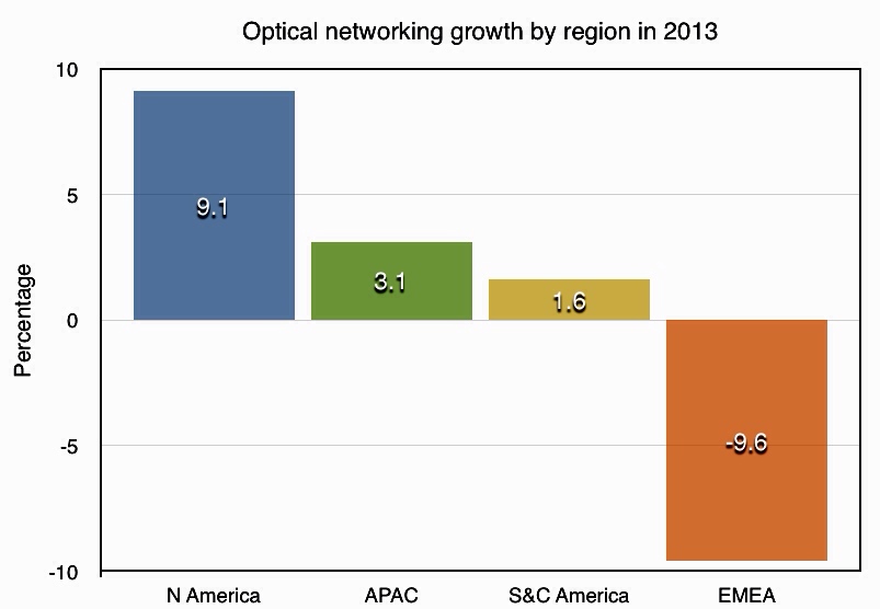
Optical networking spending up in all regions except Europe
 Source data: Ovum
Ovum forecasts that the global optical networking market will grow to US $17.5 billion by 2018, a compound annual growth rate of 3.1 percent.
Optical networking spending in North America will be up 9.1 percent in 2013 after two flat years. North American tier-1 service providers and cable operators are investing in the core network to support all traffic types, and 100 Gigabit is being deployed in volume.
In contrast, optical networking sales in EMEA will contract by nearly 10 percent in 2013. “Non-spending in Europe is the major factor in the overall EMEA decline,” says Ian Redpath, principal analyst, network infrastructure at Ovum.
The major technology trend for this forecast is the ascendancy of 100 Gig, whose sales exceeded 40 Gig revenues in 2Q13
EMEA optical networking spending has been down in four out of the past five years, and the lack of investment is becoming acute, says Ovum. Given that service providers are stretching their existing networks, spending will have to take place eventually to make up for the prolonged period of inactivity.
This year has seen 100 Gigabit become the wavelength of choice for large WDM systems, with sales surging. Spending on 100 Gigabit has now overtaken spending on 40 Gigabit which declined in the first half of the year.
"The major technology trend for this forecast is the ascendancy of 100 Gig, whose sales exceeded 40 Gig revenues in 2Q13," says Redpath.
Further reading:
Ovum: Optical networks forecast: top line steady, 100G surging, click here
u2t Photonics pushes balanced detectors to 70GHz
- u2t's 70GHz balanced detector supports 64Gbaud for test and measurement and R&D
- The company's gallium arsenide modulator and next-generation receiver will enable 100 Gigabit long-haul in a CFP2

"The performance [of gallium arsenide] is very similar to the lithium niobate modulator"
Jens Fiedler, u2t Photonics
u2t Photonics has announced a balanced detector that operates at 70GHz. Such a bandwidth supports 64 Gigabaud (Gbaud), twice the symbol rate of existing 100 Gigabit coherent optical transmission systems.
The German company announced a coherent photo-detector capable of 64Gbaud in 2012 but that had an operating bandwidth of 40GHz. The latest product uses two 70GHz photo-detectors and different packaging to meet the higher bandwidth requirements.
"The achieved performance is a result of R&D work using our experience with 100GHz single photo-detectors and balanced detector technology at a lower speed,” says Jens Fiedler, executive vice president sales and marketing at u2t Photonics.
The monolithically-integrated balanced detector has been sampling since March. The markets for the device are test and measurement systems and research and development (R&D). "It will enable engineers to work on higher-speed interface rates for system development," says Fiedler.
The balanced detector could be used in next-generation transmission systems operating at 64 Gbaud, doubling the current 100 Gigabit-per-second (Gbps) data rate while using the same dual-polarisation, quadrature phase-shift keying (DP-QPSK) architecture.
A 64Gbaud DP-QPSK coherent system would halve the number of super-channels needed for 400Gbps and 1 Terabit transmissions. In turn, using 16-QAM instead of QPSK would further halve the channel count - a single dual-polarisation, 16-QAM at 64Gbaud would deliver 400Gbps, while three channels would deliver 1.2Tbps.
However, for such a system to be deployed commercially the remaining components - the modulator, device drivers and the DSP-ASIC - would need to be able to operate at twice the 32Gbaud rate; something that is still several years out. That said, Fiedler points out that the industry is also investigating baud rates in between 32 Gig and 64 Gig.
Gallium arsenide modulator
u2t acquired gallium arsenide modulator technology in June 2009, enabling the company to offer coherent transmitter as well as receiver components.
At OFC/NFOEC 2013, u2t Photonics published a paper on its high-speed gallium arsenide coherent modulator. The company's design is based on the Mach-Zehnder modulator specification of the Optical Internetworking Forum (OIF) for 100 Gigabit DP-QPSK applications.
The DP-QPSK optical modulation includes a rotator on one arm and a polarisation beam combiner at the output. u2t has decided to support an OIF compatible design with a passive polarisation rotator and combiner which could also be integrated on chip. The resulting coherent modulator is now being tested before being integrated with the free space optics to create a working design.
"The performance [of gallium arsenide] is very similar to the lithium niobate modulator," says Fiedler. "Major system vendors have considered the technology for their use and that is still ongoing."
The gallium arsenide modulator is considerably smaller than the equivalent lithium niobate design. Indeed u2t expects the technology's power and size requirements, along with the company's coherent receiver, to fit within the CFP2 optical module. Such a pluggable 100 Gigabit coherent module would meet long-haul requirements, says Fiedler.
The gallium arsenide modulator can also be used within the existing line-side 100 Gigabit 5x7-inch MSA coherent transponder. Fiedler points out that by meeting the OIF specification, there is no space saving benefit using gallium arsenide since both modulator technologies fit within the same dimensioned package. However, the more integrated gallium arsenide modulator may deliver a cost advantage, he says.
Another benefit of using a gallium arsenide modulator is its optical performance stability with temperature. "It requires some [temperature] control but it is stable," says Fiedler.
Coherent receiver
u2t's current 100Gbps coherent receiver product uses two chips, each comprising the 90-degree hybrid and a balanced detector. "That is our current design and it is selling in volume," says Fiedler. "We are now working on the next version, according to the OIF specification, which is size-reduced."
The resulting single-chip design will cost less and fit within a CFP2 pluggable module.
The receiver might be small enough to fit within the even smaller CFP4 module, concludes Fiedler.
Software-defined networking: A network game-changer?
OFC/NFOEC reflections: Part 1

"We [operators] need to move faster"
Andrew Lord, BT
Q: What was your impression of the show?
A: Nothing out of the ordinary. I haven't come away clutching a whole bunch of results that I'm determined to go and check out, which I do sometimes.
I'm quite impressed by how the main equipment vendors have moved on to look seriously at post-100 Gigabit transmission. In fact we have some [equipment] in the labs [at BT]. That is moving on pretty quickly. I don't know if there is a need for it just yet but they are certainly getting out there, not with live chips but making serious noises on 400 Gig and beyond.
There was a talk on the CFP [module] and whether we are going to be moving to a coherent CFP at 100 Gig. So what is going to happen to those prices? Is there really going to be a role for non-coherent 100 Gig? That is still a question in my mind.
"Our dream future is that we would buy equipment from whomever we want and it works. Why can't we do that for the network?"
I was quite keen on that but I'm wondering if there is going to be a limited opportunity for the non-coherent 100 Gig variants. The coherent prices will drop and my feeling from this OFC is they are going to drop pretty quickly when people start putting these things [100 Gig coherent] in; we are putting them in. So I don't know quite what the scope is for people that are trying to push that [100 Gigabit direct detection].
What was noteworthy at the show?
There is much talk about software-defined networking (SDN), so much talk that a lot of people in my position have been describing it as hype. There is a robust debate internally [within BT] on the merits of SDN which is essentially a data centre activity. In a live network, can we make use of it? There is some skepticism.
I'm still fairly optimistic about SDN and the role it might have and the [OFC/NFOEC] conference helped that.
I'm expecting next year to be the SDN conference and I'd be surprised if SDN doesn't have a much greater impact then [OFC/NFOEC 2014] with more people demoing SDN use cases.
Why is there so much excitement about SDN?
Why now when it could have happened years ago? We could have all had GMPLS (Generalised Multi-Protocol Label Switching) control planes. We haven't got them. Control plane research has been around for a long time; we don't use it: we could but we don't. We are still sitting with heavy OpEx-centric networks, especially optical.
"The 'something different' this conference was spatial-division multiplexing"
So why are we getting excited? Getting the cost out of the operational side - the software-development side, and the ability to buy from whomever we want to.
For example, if we want to buy a new network, we put out a tender and have some 10 responses. It is hard to adjudicate them all equally when, with some of them, we'd have to start from scratch with software development, whereas with others we have a head start as our own management interface has already been developed. That shouldn't and doesn't need to be the case.
Opening the equipment's north-bound interface into our own OSS (operating systems support) in theory, and this is probably naive, any specific OSS we develop ought to work.
Our dream future is that we would buy equipment from whomever we want and it works. Why can't we do that for the network?
We want to as it means we can leverage competition but also we can get new network concepts and builds in quicker without having to suffer 18 months of writing new code to manage the thing. We used to do that but it is no longer acceptable. It is too expensive and time consuming; we need to move faster.
It [the interest in SDN] is just competition hotting up and costs getting harder to manage. This is an area that is now the focus and SDN possibly provides a way through that.
Another issue is the ability to put quickly new applications and services onto our networks. For example, a bank wants to do data backup but doesn't want to spend a year and resources developing something that it uses only occasionally. Is there a bandwidth-on-demand application we can put onto our basic network infrastructure? Why not?
SDN gives us a chance to do something like that, we could roll it out quickly for specific customers.
Anything else at OFC/NFOEC that struck you as noteworthy?
The core networks aspect of OFC is really my main interest.
You are taking the components, a big part of OFC, and then the transmission experiments and all the great results that they get - multiple Terabits and new modulation formats - and then in networks you are saying: What can I build?
The networks have always been the poor relation. It has not had the great exposure or the same excitement. Well, now, the network is becoming centre stage.
As you see components and transmission mature - and it is maturing as the capacity we are seeing on a fibre is almost hitting the natural limit - so the spectral efficiency, the amount of bits you can squeeze in a single Hertz, is hitting the limit of 3,4,5,6 [bit/s/Hz]. You can't get much more than that if you want to go a reasonable distance.
So the big buzz word - 70 to 80 percent of the OFC papers we reviewed - was flex-grid, turning the optical spectrum in fibre into a much more flexible commodity where you can have wherever spectrum you want between nodes dynamically. Very, very interesting; loads of papers on that. How do you manage that? What benefits does it give?
What did you learn from the show?
One area I don't get yet is spatial-division multiplexing. Fibre is filling up so where do we go? Well, we need to go somewhere because we are predicting our networks continuing to grow at 35 to 40 percent.
Now we are hitting a new era. Putting fibre in doesn't really solve the problem in terms of cost, energy and space. You are just layering solutions on top of each other and you don't get any more revenue from it. We are stuffed unless we do something different.
The 'something different' this conference was spatial-division multiplexing. You still have a single fibre but you put in multiple cores and that is the next way of increasing capacity. There is an awful lot of work being done in this area.
I gave a paper [pointing out the challenges]. I couldn't see how you would build the splicing equipment, how you would get this fibre qualified given the 30-40 years of expertise of companies like Corning making single mode fibre, are we really going to go through all that again for this new fibre? How long is that going to take? How do you align these things?
"SDN for many people is data centres and I think we [operators] mean something a bit different."
I just presented the basic pitfalls from an operator's perspective of using this stuff. That is my skeptic side. But I could be proved wrong, it has happened before!
Anything you learned that got you excited?
One thing I saw is optics pushing out.
In the past we saw 100 Megabit and one Gigabit Ethernet (GbE) being king of a certain part of the network. People were talking about that becoming optics.
We are starting to see optics entering a new phase. Ten Gigabit Ethernet is a wavelength, a colour on a fibre. If the cost of those very simple 10GbE transceivers continues to drop, we will start to see optics enter a new phase where we could be seeing it all over the place: you have a GigE port, well, have a wavelength.
[When that happens] optics comes centre stage and then you have to address optical questions. This is exciting and Ericsson was talking a bit about that.
What will you be monitoring between now and the next OFC?
We are accelerating our SDN work. We see that as being game-changing in terms of networks. I've seen enough open standards emerging, enough will around the industry with the people I've spoken to, some of the vendors that want to do some work with us, that it is exciting. Things like 4k and 8k (ultra high definition) TV, providing the bandwidth to make this thing sensible.
"I don't think BT needs to be delving into the insides of an IP router trying to improve how it moves packets. That is not our job."
Think of a health application where you have a 4 or 8k TV camera giving an ultra high-res picture of a scan, piping that around the network at many many Gigabits. These type of applications are exciting and that is where we are going to be putting a bit more effort. Rather than the traditional just thinking about transmission, we are moving on to some solid networking; that is how we are migrating it in the group.
When you say open standards [for SDN], OpenFlow comes to mind.
OpenFlow is a lovely academic thing. It allows you to open a box for a university to try their own algorithms. But it doesn't really help us because we don't want to get down to that level.
I don't think BT needs to be delving into the insides of an IP router trying to improve how it moves packets. That is not our job.
What we need is the next level up: taking entire network functions and having them presented in an open way.
For example, something like OpenStack [the open source cloud computing software] that allows you to start to bring networking, and compute and memory resources in data centres together.
You can start to say: I have a data centre here, another here and some networking in between, how can I orchestrate all of that? I need to provide some backup or some protection, what gets all those diverse elements, in very different parts of the industry, what is it that will orchestrate that automatically?
That is the kind of open theme that operators are interested in.
That sounds different to what is being developed for SDN in the data centre. Are there two areas here: one networking and one the data centre?
You are quite right. SDN for many people is data centres and I think we mean something a bit different. We are trying to have multi-vendor leverage and as I've said, look at the software issues.
We also need to be a bit clearer as to what we mean by it [SDN].
Andrew Lord has been appointed technical chair at OFC/NFOEC
Further reading
Part 2: OFC/NFOEC 2013 industry reflections, click here
Part 3: OFC/NFOEC 2013 industry reflections, click here
Part 4: OFC/NFOEC industry reflections, click here
Part 5: OFC/NFEC 2013 industry reflections, click here
Luxtera's interconnect strategy
Part 1: Optical interconnect
Luxtera demonstrated a 100 Gigabit QSFP optical module at the OFC/NFOEC 2013 exhibition.
 "We're in discussions with a lot of memory vendors, switch vendors and different ASIC providers"
Chris Bergey, Luxtera
The silicon photonics-based QSFP pluggable transceiver was part of the Optical Internetworking Forum's (OIF) multi-vendor demonstration of the 4x25 Gigabit chip-to-module interface, defined by the CEI-28G-VSR Implementation Agreement.
The OIF demonstration involved several optical module and chip companies and included CFP2 modules running the 100GBASE-LR4 10km standard alongside Luxtera's 4x28 Gigabit-per-second (Gbps) silicon photonics-based QSFP28.
Kotura also previewed a 100Gbps QSFP at OFC/NFOEC but its silicon photonics design uses two chips and wavelength-division multiplexing (WDM).
The Luxtera QSFP28 is being aimed at data centre applications and has a 500m reach although Luxtera says up to 2km is possible. The QSFP28 is sampling to initial customers and will be in production next year.
100 Gigabit modules
Current 100GBASE-LR4 client-side interfaces are available in the CFP form factor. OFC/NFOEC 2013 saw the announcement of two smaller pluggable form factors at 100Gbps: the CFP2, the next pluggable on the CFP MSA roadmap, and Cisco Systems' in-house CPAK.
Now silicon photonics player Luxtera is coming to market with a QSFP-based 100 Gigabit interface, more compact than the CFP2 and CPAK.
The QSFP is already available as a 40Gbps interface. The 40Gbps QSFP also supports four independent 10Gbps interfaces. The QSFP form factor, along with the SFP+, are widely used on the front panels of data centre switches.
"The QSFP is an inside-the-data-centre connector while the CFP/CFP2 is an edge of the data centre, and for telecom, an edge router connector," says Chris Bergey, vice president of marketing at Luxtera. "These are different markets in terms of their power consumption and cost."
Bergey says the big 'Web 2.0' data centre operators like the reach and density offered by the 100Gbps QSFP as their data centres are physically large and use flatter, less tiered switch architectures.
"If you are a big systems company and you are betting on your flagship chip, you better have multiple sources"
The content service providers also buy transceivers in large volumes and like that the Luxtera QSFP works over single-mode fibre which is cheaper than multi-mode fibre. "All these factors lead to where we think silicon photonics plays in a big way," says Bergey.
The 100Gbps QSFP must deliver a lower cost-per-bit compared to the 40Gbps QSFP if it is to be adopted widely. Luxtera estimates that the QSFP28 will cost less than US $1,000 and could be as low as $250.
Optical interconnect
Luxtera says its focus is on low-cost, high-density interconnect rather than optical transceivers. "We want to be a chip company," says Bergey.
The company defines optical interconnect as covering active optical cable and transceivers, optical engines used as board-mounted optics placed next to chips, and ASICs with optical SerDes (serialiser/ deserialisers) rather than copper ones.
Optical interconnect, it argues, will have a three-stage evolution: starting with face-plate transceivers, moving to mid-board optics and then ASICS with optical interfaces. Such optical interconnect developments promise lower cost high-speed designs and new ways to architect systems.
Currently optics are largely confined to transceivers on a system׳s front panel. The exceptions are high-end supercomputer systems and emerging novel designs such as Compass-EOS's IP core router.
"The problem with the front panel is the density you can achieve is somewhat limited," says Bergey. Leading switch IC suppliers using a 40nm CMOS process are capable of a Terabit of switching. "That matches really well if you put a ton of QSFPs on the front panel," says Bergey.
But once switch IC vendors use the next CMOS process node, the switching capacity will rise to several Terabits. This becomes far more challenging to meet using front panel optics and will be more costly compared to putting board-mounted optics alongside the chip.
"When we build [silicon photonics] chips, we can package them in QSFPs for the front panel, or we can package them for mid-board optics," says Bergey.
"If it [silicon photonics] is viewed as exotic, it is never going to hit the volumes we aspire to."
The use of mid-board optics by system vendors is the second stage in the evolution of optical interconnect. "It [mid-board optics] is an intermediate step between how you move from copper I/O [input/output] to optical I/O," says Bergey.
The use of mid-board optics requires less power, especially when using 25Gbps signals, says Bergey: “You dont need as many [signal] retimers.” It also saves power consumed by the SerDes - from 2W for each SerDes to 1W, since the mid-board optics are closer and signals need not be driven all the way to the front panel. "You are saving 2W per 100 Gig and if you are doing several Terabits, that adds up," says Bergey.
The end game is optical I/O. This will be required wherever there are dense I/O requirements and where a lot of traffic is aggregated.
Luxtera, as a silicon photonics player, is pursuing an approach to integrate optics with VLSI devices. "We're in discussions with a lot of memory vendors, switch vendors and different ASIC providers," says Bergey.
Silicon photonics fab
Last year STMicroelectronics (ST) and Luxtera announced they would create a 300mm wafer silicon photonics process at ST's facility in Crolles, France.
Luxtera expects that line to be qualified, ramped and in production in 2014. Before then, devices need to be built, qualified and tested for their reliability.
"If you are a big systems company and you are betting on your flagship chip, you better have multiple sources," says Bergey. "That is what we are doing with ST: it drastically expands the total available market of silicon photonics and it is something that ST and Luxtera can benefit from.”
Having multiple sources is important, says Bergey: "If it [silicon photonics] is viewed as exotic, it is never going to hit the volumes we aspire to."
Part 2: Bell Labs on silicon photonics click here
Part 3: Is silicon photonics an industry game-changer? click here
Kotura demonstrates a 100 Gigabit QSFP
 “QSFP will be the long-term winner at 100 Gig; the same way QSFP has been a high volume winner at 40 Gig”
Arlon Martin, Kotura
The device is aimed at plugging the gap between vertical-cavity surface-emitting laser (VCSEL) -based 100GBASE-SR10 designs that have span 100m, and the CFP-based 100GBASE-LR4 that has a 10km reach.
“It is aimed at the intermediate space, which the IEEE is looking at a new standard for," says Arlon Martin, vice president of marketing at Kotura.
The device is similar to Luxtera's 100 Gigabit-per-second (Gbps) QSFP, also detailed at the OFC/NFOEC 2013 exhibition, and is targeting the same switch applications in the data centre. “Where we differ is our ability to do wavelength-division multiplexing (WDM) on a chip,” says Martin. Kotura also uses third-party electronics such as laser drivers and transimpedance amplifiers (TIA) whereas Luxtera develops and integrates its own.
The Kotura QSFP uses four wavelengths, each at 25Gbps, that operate around 1550nm. “We picked 1550nm because that is where a lot of the WDM applications are," says Martin. “There are also some customers that want more than four channels.” The company says it is also doing development work at 1310nm.
Although Kotura's implementation doesn't adhere to an IEEE standard - the standard is still work in progress - Martin points out that the 10x10 MSA is also not an IEEE standard, yet is probably the best selling client-side 100Gbps interface.
Optical component and module vendors including Avago Technologies, Finisar, Oclaro, Oplink, Fujitsu Optical Components and NeoPhotonics all announced CFP2 module products at OFC/NFOEC 2013. The CFP2 is the next pluggable form factor on the CFP MSA roadmap and is approximately half the size of the CFP.
The advent of the CFP2 enables eight 100Gbps pluggable modules on a system's front panel compared to four CFPs. But with the QSFP, up to 24 modules can be fitted while 48 are possible when mounted double sidedly - ’belly-to-belly’ - across the panel. “QSFP will be the long-term winner at 100 Gig; the same way QSFP has been a high volume winner at 40 Gig,” says Martin.
The QSFP uses 28Gbps pins, which is also called the QSFP28, but Kotura refers to it 100Gbps product as a QSFP. The design consumes 3.5W and uses two silicon photonic chips. Kotura says 80 percent of the total power consumption is due to the electronics.
One of the two chips is the silicon transmitter which houses the platform for the four lasers (gain chips) combined as a four-channel array. Each is an external cavity laser where part of the cavity is within the indium phosphide device and the rest in the silicon photonics waveguide. The gain chips are flip-chipped onto the silicon. The transmitter also includes a grating that sets each laser's wavelength, four modulators, and a WDM multiplexer to combine the four wavelengths before transmission on the fibre.
 Kotura's 4x25 Gig transmitter and receiver chips. Source: Kotura
The receiver chip uses a four-channel demultiplexer with each channel fed to a germanium photo-detector. Two chips are used as it is easier to package each as a transmitter optical sub-assembly (TOSA) or receiver optical sub-assembly (ROSA), says Martin. The 100Gbps QSFP will be generally available in 2014.
Disruptive system design
The recent Compass-EOS IP router announcement is a welcome development, says Kotura, as it brings the optics inside the system - an example of mid-board optics - as opposed to the front panel. Compass-EOS refers to its novel icPhotonics chip combining a router chip and optics as silicon photonics but in practice it is an integrated optics design. The 168 VCSELs and 168 photodetectors per chip is massively parallel interconnect, says Martin.
“The advantage, from our point of view of silicon photonics, is to do WDM on the same fibre in order to reduce the amount of cabling and interconnect needed,” he says. At 100 Gigabit this reduces the cabling by a factor of four and this will grow with more 25Gbps wavelength channels used to 10x or even 40x eventually.
“What we want to do is transition from the electronics to the optical domain as close to those large switching chips as possible,” says Martin. “Pioneers [like Compass-EOS] demonstrating that style of architecture are to be welcomed."
Kotura says that every company that is building large switching and routing ASICs is looking at various interface options. "We have talked to quite a few of them,” says Martin.
One solution suited to silicon photonics is to place the lasers on the front panel while putting the modulation, detection and WDM devices - packaged using silicon photonics - right next to the ASICs. This way the laser works at the cooler room temperature while the rest of the circuitry can be at the temperature of the chip, says Martin.