
Silicon photonics has reached an inflexion point, says Kevin Soukup, senior vice president at GlobalFoundries’ silicon photonics business, who points out that the foundry is fielding new enquiries.
“We see customers that don’t have an optics strategy coming to GlobalFoundries now,” says Kevin Soukup. “Even if they don’t have a photonics design team, they want to engage to build out their optical strategy.”
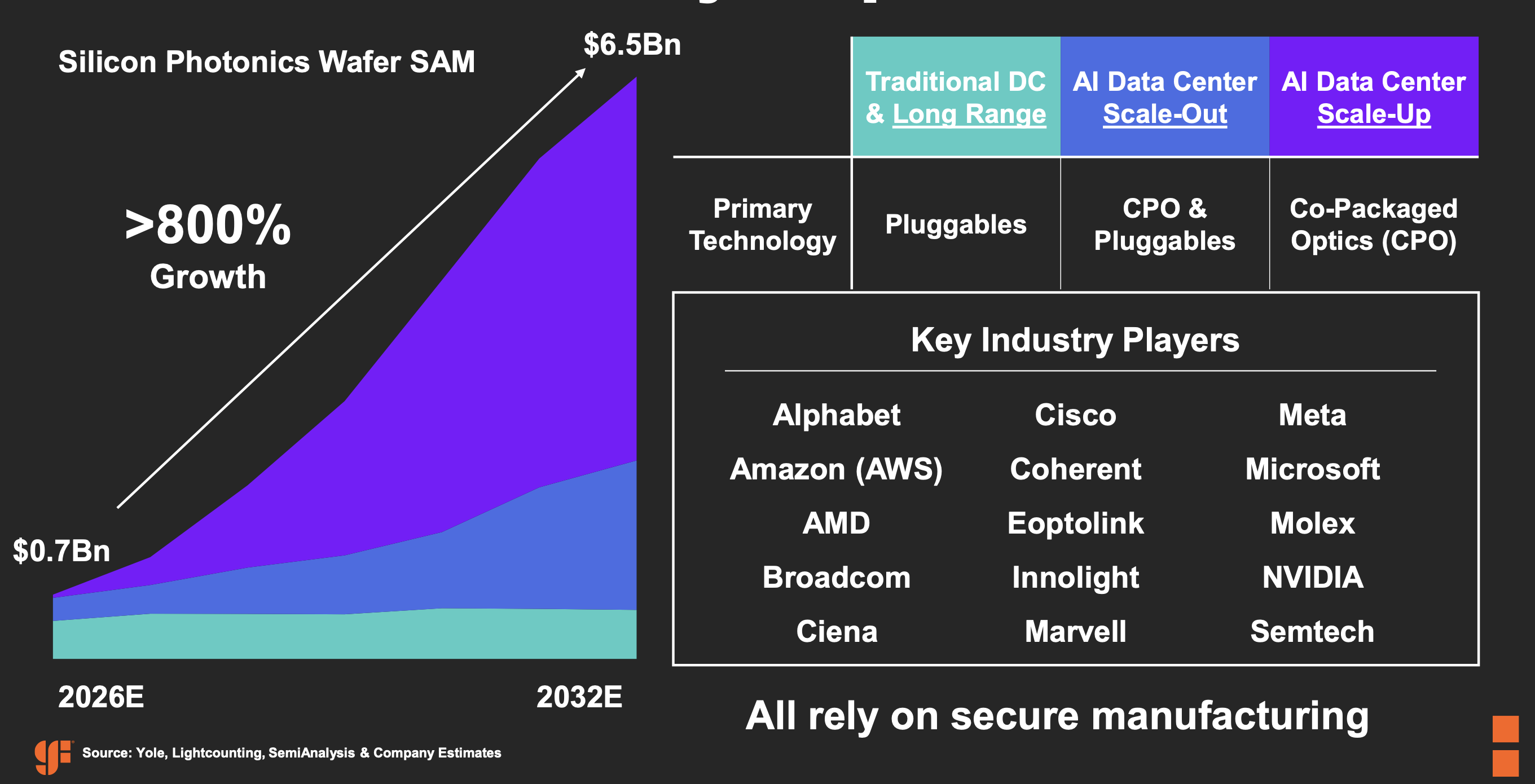
The shift marks a decisive change from a year ago, when the industry was still debating the scale of silicon photonics’ adoption. That debate, says Soukup, has been settled by a wave of co-packaged optics announcements and an insatiable demand for bandwidth driven by AI data centre build-outs.
And GlobalFoundries has recently acquired Advanced Micro Foundry (AMF). The deal places GlobalFoundries at the top in terms of silicon photonics revenue, but it will certainly re-energise the competition, said LightCounting Market Research in a research note published last November.
AMF acquisition
Buying Singapore-based AMF is central to GlobalFoundries’ ambitions. “AMF brings a whole set of different customers,” says Soukup. One of AMF’s strengths lies in coherent optics for long-haul applications, which Soukup says exceeds what GlobalFoundries had achieved independently.
AMF’s team has built a successful business, supporting more than 300 customers, mostly in Asia, developing silicon photonics products across a range of applications, including optical communications, says LightCounting.
AMF has also been working to bring in optical modulator materials and to integrate indium phosphide laser chips onto silicon – critical technologies for staying ahead of the competition. For example, for 400 gigabit technology, AMF has been using thin-film lithium niobate and polymer-based modulator approaches.
The combined R&D teams, bolstered by A*STAR’s broader resources in Singapore, are now focused on a unified roadmap spanning pluggables, co-packaged optics, and emerging markets, including quantum computing, LIDAR, and automotive connectivity.
There is also another dimension to the deal. AMF operated on a government research site with limited room to expand, which constrained its ability to win customers that required volume production. “There are a lot of customers that liked AMF’s technology but never saw a path to scale,” says Soukup.
GlobalFoundries’ own campus in Singapore, with its large-scale 200mm and 300mm wafer capacity, removes that constraint. The plan is to offer AMF’s customers a transition path into a high-volume manufacturing environment.
Meeting market needs
For pluggable transceivers, activity is intense, says Soukup, as transceiver companies develop higher-speed devices.
“We see quite a bit of adoption in the scale-out section of the market, so many different pluggable transceiver companies coming looking for not just 200 gigabit-per-lane products, which are in qualification stage now, but 400 gigabit per lane,” he says. A 200-gigabit-per-lane solution enables 1.6 terabit-per-second (Tbps) pluggables using eight lanes.
Interest extends to 400 gigabit-per-second (Gbps) and 800Gbps coherent single-wavelength pluggable solutions, with the 800ZR+ emerging as a focal point for extended-reach applications. “That’s the direction that we see: ZR+,” says Soukup.
The coherent long-haul market is also evolving. Once confined to telecom networks, coherent optics are now being deployed for ‘scale-across’ networking applications, sharing large AI workloads across data centres.
Evolving role
For pluggables, a high-bandwidth optical modulator capable of supporting 200 gigabits per lane is the entry point. For co-packaged optics, requirements go further: through-silicon vias (TSVs) that support an electronic IC stacked on the photonic IC, with high-density pitch for both power and to ensure signal integrity.
“Many of the electronic IC companies are seeking more digital scaling, and so the ability to support, for example, a 3nm EIC with a high-density pitch of TSVs — that advanced packaging roadmap is really important,” says Soukup.
Fibre attach is also critical. GlobalFoundries is developing a broadband detachable fibre approach that supports multiple wavelengths, an essential capability as the industry moves beyond single-wavelength architectures toward four-lambda and eventually sixteen-lambda designs.
“That allows the technology to scale beyond single wavelength, and we expect bandwidth to rise exponentially,” says Soukup.
He is candid about the state of play: the fibre-attach landscape remains fragmented, with vendors pursuing different approaches—current solutions based on edge coupling work for one or two wavelengths but won’t scale to sixteen.
“Over the next five-plus years, fibre attach is going to change a lot before we reach a standard solution that works for everyone, and we may never get there,” he says.
Monolithic heritage
GlobalFoundries’ heritage in silicon photonics is rooted in monolithic integration—the ability to combine CMOS, radio-frequency circuitry, and silicon photonics on a single chip.
The approach works for certain customers, including those that address LIDAR and pluggable transceivers. GlobalFoundries also offers embedding heater-control circuitry directly on-chip to manage thermal effects that can affect optical performance.
But the foundry recognises its limits. “For some applications, they need more digital horsepower than the monolithic integration supports,” says Soukup, i.e. advanced CMOS process nodes.
GlobalFoundries now supports this with a photonics-only flow alongside its monolithic option: a simpler process with fewer mask steps and lower cycle time, yet one that supports the full advanced packaging stack, including electronic IC stacking and cavity-based fibre attach.
Customers can bring an advanced node electronic IC from another CMOS foundry and co-package it with a GlobalFoundries PIC. The company also has a customer fabricating an electronic IC on its own 22FDX platform.
Modulators
The question of new modulator materials — thin-film lithium niobate, barium titanate, advanced polymers — looms large over the industry’s roadmap for higher baud rates.
Soukup describes the modulator work as pathfinding. The challenge is twofold: can the supply chain scale, and can the new material be encapsulated and integrated without destabilising existing processes?
Development work happens off-site, with coupons and, eventually, full wafers brought in for bonding to GlobalFoundries silicon. “That’s part of the development — can you encapsulate it properly, and can you industrialise that solution? It’s an open question,” he says.
Customisation versus standardisation
A decade of work with universities, consortia, and start-ups generated a wealth of process variants, but at some point, GlobalFoundries had to narrow its focus and industrialise. “There was a time when we started to turn away customers who required customisation,” says Soukup.
That phase is now largely behind the company. The aperture is widening again, though the nature of the customisation has changed: it is more about specific device tweaks and implant set-ups than wholesale process re-architecture. Even so, Soukup notes every customer who downloads the process development kit (PDK) typically asks for something special. “They all have some special sauce that they want.”
Soukup also draws an analogy with the CMOS world. Just as mature semiconductor nodes at 40nm, 28nm, and even older 130nm processes continue to serve high-volume applications long after leading-edge development has moved on, silicon photonics will develop its own hierarchy of maturity.
Edge-coupled fibre attach will serve certain applications; broadband surface-mount detachable solutions will serve others. Modulator and photodiode technologies will follow a similar trajectory.
“Parts of the market will commoditise,” says Soukup. “They’ll reach a level of maturity. They’ll support applications that don’t need that innovation. And then other parts of the market will continue to drive very aggressively to the next greatest thing.”
Pushing silicon photonics
Is silicon photonics settling down? Far from it, says Soukup.
The technology is undergoing what he characterises as leading-edge development, with fibre attach, modulators, photodiodes, electronic IC architectures, and advanced packaging all in active pathfinding.
The AI data centre build-out is accelerating demand, and co-packaged optics for scale-up interconnects could shift the market into a different gear within a few years.
GlobalFoundries, now the largest pure-play silicon photonics foundry following the AMF deal, is betting that its combination of 300mm wafer manufacturing scale, monolithic and heterogeneous integration options, and an advanced photonics and packaging centre in New York will position it at the centre of what Soukup calls the most interesting period the industry has seen.