
The markets for photonic integrated circuits in 2030
What will be the leading markets for photonic integrated circuits (PICs) by the decade’s end? And what are the challenges facing the PIC industry?
A panel session at the recent PIC Summit Europe event held in Eindhoven, The Netherlands, looked at what would be the markets for photonic integrated circuits by 2030.
The market for PICs is dominated by datacom and telecom. However, emerging applications include medical and wearable devices, optical computing, autonomous vehicles, and sensing applications for the oil, gas, water, and agriculture industries.
Taking part in the PIC Summit Europe panel on behalf of LightCounting Market Research, I shared two forecast charts. One showed LightCounting’s latest Ethernet module forecast, highlighting the rapid growth expected in the next five years, including the adoption of 1.6-terabit and 3.2-terabit pluggables. Also shown was how silicon photonics is gaining market share and will account for nearly half of all optical transceivers by 2029.
No surprise then that LightCounting’s view is that datacom and telecom will remain the dominant markets for PICs in 2030. Moreover, the challenges AI is posing the optical industry means the photonics developments will continue to drive the PIC market overall.


Before the PIC Summit Europe panel, Gazettabyte sought some industry views. What would help the PIC landscape, and what should the PIC industry be addressing? Also, what were the views regarding the PIC marketplace in 2030?
Those approached focus mainly on datacom and telecom. But Julie Eng, the CTO of Coherent, has a broader remit that includes emerging photonics markets, while Mehdi Asghari is CEO of SiLC Technologies, a silicon photonics start-up focused on the Lidar marketplace.
Emerging PIC markets
Dave Welch, founder of Infinera and now founder and CEO of stealth start-up AttoTude, says PICs for datacom and telecom are alive and thriving, while PICs for Lidar and sensing are burgeoning applications with real volume.


“Datacom and telecom will dominate for the foreseeable future,” says Welch. “I do not see where any other application of comparable size can come from.”
Maxim Kuschnerov, director of R&D, points out that 2030 is not as far out as it used to be: “That is like two bigger product cycles at most.” He, too, says datacom and telecom will remain the main markets for PICs.
Coherent’s Eng agrees: “The primary driver of PICs will be datacom and telecom, but if you’re looking for additional drivers, health monitoring is a possible one.”
Coherent experienced an uptick for optical components for medical equipment during the COVID-19 pandemic. “The pandemic increased demand for PCR [polymerase chain reaction] testing, which grew the business for products we sell, such as optical filters and thermoelectric coolers,” says Eng. “The pandemic focused people more on health monitoring, and that, combined with advanced health-monitoring featured in smart-watches, has grown interested in personal health monitoring.”
Eng notes that component sales into PCR testing declined post-COVID although interest remains high in personal health monitoring.
Companies are also addressing biosensing using silicon photonics and semiconductor lasers. “In some cases, a silicon photonics PIC for this application could be fairly large as it is often helpful to monitor many wavelengths,” says Eng. She also highlights potential volumes. “If biosensing in the watch takes off, that could be a higher volume than datacom transceivers, and the PICs may be large. So that is an application to watch.”


“The pandemic experience has pushed the point-of-care testing market, which include biosensors, exponentially,” says Professor Laura Lechuga, a leading biosensor researcher. “This is an increasing market every year with an intensive research and development at academic and industrial level. Point-of-care will be for sure the future of diagnostics.”
Kuschnerov also highlights the health-monitoring market. “There has been a lot of work on non-invasive glucose monitoring using optical sensing, but it is not clear if this could pass FDA [U.S. Food and Drug Agency] approval,” says Kuschnerov. “It could be a life changer for people with diabetes.”
Rafik Ward is a consultant working with companies on PIC developments including the point-of-care medical device marketplace. One start-up developing PIC technology realised it was competing with low-cost point-of-care diagnostics devices. Another challenge the start-up faced is the long development cycles and difficulty entering the medical marketplace. The start-up decided to refocus on communications.
“One thing that did come from COVID was the realisation of how fragile our distribution and logistics ecosystem was and how dependent it was on low-cost labour,” says SiLC’s Asghari. The labour shortage persisted after COVID-19 and has driven a push for warehouse and logistic automation. “For our business in Lidar, this has created a significant demand in robotics and automation,” says Asghari.
Another driver is the drop in the working-age population—about 1 per cent a year—caused by the drop in population growth in industrial countries over the past 20 years.
“This is a major issue and is becoming even more critical over time,” says Asghari. “If robots need to do the kind of work that people do, then they need to see the way we do, and cameras and even 3D imagers don’t cut it.”
Kuschnerov says gas, oil, water quality, and agriculture will eventually use optical sensing variants, but he does not expect high volumes.

Another wearable market is augmented reality/ virtual reality (AR/VR) glasses. This volume market has been predicted for years, but work is taking place, such as the development of diffractive waveguides for such glasses. “Research is happening here, which can’t be ignored, but it’s a non-existent market today,” says Kuschnerov.
Infra-red sensors are set to grow for autonomous drone warfare. Military drones being used in Ukraine and the Middle East are changing modern warfare, he says, a development noted by the leading militaries.
VCSELs for a 3D vision of robots will continue to stay relevant. “The future is full of these (Tesla-like) robots. I’m sure they will need VCSEL arrays,” says Kuschnerov.
Challenges facing the PIC industry
Ward says the highest priority regarding PICs is for the fabrication plants [fabs] to reduce cycle times from tape-out to returned chips.


Indium phosphide fabs regularly turn around chips in six to eight weeks, whereas several of the big silicon photonics fabs take five months. Moreover, chip designs can often take two to three iterations to get to production. “We shouldn’t be surprised that indium phosphide has consistently been six or more months ahead of silicon photonics at each generation,” says Ward. “It’s simple maths.” Silicon photonics needs to be developed to launch new generations of communication devices at the same time as indium phosphide products.
Ward also highlights the need for improved process design kits (PDKs). “While this is improving, there is still too much redundant work by PIC customers because PDKs are immature,” he says.
AttoTude’s Welch notes that, in years past, the value of PICs has been in integrating optics, specifically lasers. The issue with lasers, however, is their environmental compatibility with silicon circuits. “This problem needs to be improved if we expect greater integration into the system needs,” says Welch.
Prof. Lechuga says that one of the main obstacles for biosensors is mass-fabrication at low cost. “It will be interested to see if Europe could offer such fabrication,” she says.
Another issue is the benefits a PIC brings. For Eng, PICs must solve a problem and offer value at a lower cost than existing solutions. “That is a big ask,” says Eng. “Optical technologists must understand new markets with many established technologies.”
Getting help
Asghari suggests several ways the optics industry and governments can help, and not just for PICs. The industry and governments must be measured to avoid boom-and-bust cycles, or at least not feed them.

“I see the AI hype now, and it brings back bitter memories of the 2000 era,” says Asghari. “That did not help anyone and set back the industry in a major way.”
He also calls for fairer trade but not through tariffs. We need fairness, he says: “Our gates are wide open, and we hold ourselves to rules that do not allow governments to support industry.”
But China does whatever it likes, he says. “Our reaction is to add tariffs on imports on things that our industry needs to manufacture, and unfortunately, a lot of these are still from China.” It is, therefore, important to make it easier for companies to manufacture in the West and help bring back basic key capabilities. “We should enable investments and not tax them, and we should stimulate the venture capital communities to invest in hardware, which no one does anymore,” says Asghari.
The issue of population shrinkage and the need for automation is the photonics industry’s chance to lead. “But we are losing again due to lack of investment in the same way that we are losing the electrical vehicle market,” he warns.
For Asghari, what is needed is a long-term vision, stability, and fairness.

ECOC 2024 industry reflections - Part III
Gazettabyte is asking industry figures for their thoughts after attending the recent 50th-anniversary ECOC show in Frankfurt. Here are contributions from Aloe Semiconductor’s Chris Doerr, Hacene Chaouch of Arista Networks, and Lumentum’s Marc Stiller.
Autumn morning near the ECOC congress centre in Frankfurt
If there was one overall message from ECOC 2024 this year, it is that incumbent technologies are winning in the communications market.
Copper is not giving up. It consumes less power and is cheaper than optics, and now, more electronics such as retimers are being applied to keep direct-attach copper (DAC) cables going. Also, 200-plus gigabaud (GBd) made a debut in coherent optics, but in intensity-modulation direct-detect (IMDD), 50GBd and 100GBd look like they are here to stay for several more years.
Pluggables are entrenching themselves more deeply. For large-scale co-packaged optics to unseat them seems further away than ever. The reason for the recent success of incumbent technologies is practicality. Large computing clusters and data centres need more bandwidth immediately, and there is not enough time to develop new technologies.
Probably the most significant practical constraint is power consumption. Communications is becoming a significant fraction of total power consumption, further driven by the desire to disaggregate to spread out the power consumption. Liquid cooling demonstrations are becoming commonplace.
Power consumption may limit the market as customers cannot obtain more power. This may mean the lowest power solution will win, making cost, complexity, and size secondary considerations.
Hacene Chaouch, Distinguished Engineer, Arista Networks
Unlike the 2023 edition, ECOC 2024 overwhelmingly and unanimously put power consumption on a pedestal.
Sleepwalking the last decade on incremental power-per-bit improvements, the AI boom has caught the optics industry off guard. Every extra Watt wasted on optics and the associated cooling systems matters since that power is not available to the Graphics Processing Units (GPUs) that generate revenue.
In this context, seeing 30W 1.6-terabit digital signal processor (DSP) optical modules demonstrated at the show floor was disappointing. This is especially so when compared to 1.6-terabit linear pluggable optics (LPO) with prototypes consuming only 10W.
The industry must and can do better to address the power gap of 1.6-terabit DSP-based optics.
Marc Stiller, Lumentum’s Vice President of Product Line Management, Cloud and Networking
ECOC 2024 saw AI emerge as a focal point for many discussions and technology drivers, continuing trends we observed at OFC earlier this year. ECOC showcased numerous new technologies and steady progress on products addressing the insatiable appetite for bandwidth.
LPO was visible, with steady advancements in performance and interoperability and a new multi-source agreement (MSA) pending. There was an overall emphasis on power efficiency and cooling solutions, driven by the increasing scale of machine learning/ AI clusters and the power availability to cool them.
Another focus was 1.6-terabit interfaces with multiple suppliers showcasing their progress. Electro-absorption modulated laser (EML) and silicon photonics solutions continue to evolve, with EMLs showing an early lead.
Other notable demonstrations emphasised breakthroughs in higher data rates and energy-efficient solutions, addressing the critical challenge of increasing memory bandwidth. Nvidia signalled their commitment to driving the pace of optics with a newly developed PAM4 DSP.
From a networking perspective, 800-gigabit is becoming the new standard, particularly with C- and L-bands gaining traction as the industry approaches the Shannon limit. Integration is more critical than ever for achieving power and cost efficiencies, especially as 800-gigabit ZR and ZR+ solutions become more prominent.
Lumentum showcased high-performance transceivers and provided critical insights into the future of networking at ECOC, reinforcing our leadership in driving these innovations forward.

Is 6G’s fate to repeat the failings of 5G wireless?
Will the telecom industry embark on another costly wireless upgrade? Telecom consultant and author William Webb thinks so and warns that it risks repeating what happened with 5G.
William Webb published the book The 5G Myth in 2016. In it, he warned that the then-emerging 5G standard would prove costly and fail to deliver on the bold promises made for the emerging wireless technology.
Webb sees history repeating itself with 6G, the next wireless standard generation. In his latest book, The 6G Manifesto, he reflects on the emerging standard and outlines what the industry and its most significant stakeholder – the telecom operators – could do instead.
Developing a new generation wireless standard every decade has proved beneficial, says Webb. However, the underlying benefits with each generation has diminished to the degree that, with 5G, it is questionable whether the latest generation was needed.
Wireless generations
There was no first-generation (1G) cellular standard. Instead, there was a mishmash of analogue cellular standards that were regional and manufacturer-specific.
The second-generation (2G) wireless standard brought technological alignment and, with it, economies of scale. Then, the 3G and the 4G standards advanced the wireless radio’s air interface. 5G was the first time the air interface didn’t change; an essential ingredient of generational change was no longer needed.
The issue now is that the wireless industry is used to new generations. But if the benefits being delivered are diminishing, who exactly is this huge undertaking serving? asks Webb. With 5G, certainly not the operators. The operators have invested heavily in rolling out 5G and may eventually see a return but that is far from their experience to date.
The wireless industry is unique in adopting a generation approach. There are no such generations for cars, aeroplanes, computers, and the internet, says Webb: “Ok, the internet went from IPv4 to IPv6, but that was an update, as and when needed.” With 5G, there was no apparent need for a new generation, he says. It wasn’t as if networks were failing, or there was a fundamental security issue. or that 4G suffered from a lack of bandwidth.
Instead, 5G was driven by academics and equipment vendors. “They postulated what some of the new applications might be,” says Webb. “Some of them were crazy guesses, the most obvious being remote surgery.” That implied a need for faster wireless links and more bandwidth. Extra bandwidth meant higher and wider radio frequency bands which came at a cost for the operators. Higher radio spectrum – above 3GHz – means greater radio signal attenuation requiring smaller-area radio cells and a greater network investment for the operators.
The industry has been working on 6G for several years. Yet, it is still early to discuss the likely outcome. Webb outlines three possible approaches for 6G: HetNets, 5G-on-steroids, and 6G in the form of software updates only.
HetNets
Webb is a proponent for operators collaborating on heterogenous networks (HetNets).
He says the idea originated with 3G but has never been adopted. The concept requires service providers to collaborate to combine disparate networks — cellular, WiFi, and satellite — to improve connectivity and coverage and ultimately improve the end-user experience.
“Perhaps this is the time to do it,” says Webb, even if he is not optimistic: operators have never backed the idea because they favour their own networks.
In the book The 6G Manifesto, Webb explores the HetNets concept, how it could be implemented and the approach’s benefits. The implementation could also be done primarily in software, which the operators favour for 6G (see below).
“They would need to remove a few things like authentication and native provisioning of voice from their networks,” says Webb. There would also need to be some form of coordinator, essentially a database-switch that could run in the cloud.
5G on steroids
The approach adopted for 5G is an application-driven approach, whereby academics and equipment vendors identified applications and their requirements and developed the necessary technologies. Such an approach for 6G, says Webb, is yet more 5G on steroids. 6G will be faster than 5G, require higher frequency spectrum and be designed to address more sectors, each with their own requirements.
“The operators understand their economics, of course, and are closer to their customers,” says Webb. It is the operators not the manufacturers that should be driving 6G.
6G as software
The third approach is for 6G to be the first cellular generation that involves software only to avoid substantial and costly hardware upgrades.
Webb says the operators have not suggested what exactly these software upgrades would do, more that after their costly 5G network upgrades, they want to avoid another cycle of expensive network investment.
Backing a software approach allows operators to avoid being seen as dragging their feet. Rather, they could point to the existing industry organisation, the GSMA, and its releases that occur every 18 months that enhance the current generation and are largely software-based. This could become the new model in future.
5G could have been avoided and simply been an upgrade to 4.5G, says Webb. With periodic releases and software updates 6G could be avoided.
But the operators need to be more vocal. However, there is no consensus among operators globally. China will deploy 6G, whatever its form. But, warns Webb, if the operators don’t step up, 6G will be forced on them. “Hence my call to arms in the book, which says to the operators: ‘If you want an outcome that is different to 5G, you need to step up’.”
A manifesto
Webb argues that the pressure and expectation from 6G wireless are so great that the likely outcome is that it will repeat what happened with 5G.
The logic that 6G is not needed and its needs served with software upgrades will not be enough to halt the momentum driving 6G. 6G will thus not help the operators reverse their fortunes and generate new growth. This is not good news given that service providers already operate in a utility market while facing fierce competition.
“If you look at most utilities – gas, electricity, water – you end up with a monopoly network supplier and then perhaps some competition around the edges,” says Webb. “Telecoms is now a utility in that each mobile operator is delivering something that towards every consumer looks indistinguishable.”
It is not good news too for the equipment vendors. Vendors may drive 6G and get one more generation of equipment sales but it is just delaying the inevitable.
Webb believes the telcos’ revenues will remain the same, resulting in a somewhat profitable businesses: “They’re making more profit than utilities but less than technology companies.”
Webb’s book ends with a manifesto for 6G.
Mobile technology underpins modern life, and having an always-present connectivity is increasingly important yet must also be affordable to all. He calls for operators to drive 6G standards and for governments to regulate in a way that benefits citizens’ connectivity services.
Users have not benefitted from 5G. If that is to change with 6G, there needs to be a clear voice that makes a wireless world better for everyone.
Further Information:
The significance of 6G, click here

First 50G-PON merchant silicon spurs operator trials
Broadcom has unveiled the industry’s first merchant silicon for the 50-gigabit passive optical network (50G-PON) access standard. Until now, only access equipment players such as Huawei and ZTE had their own 50G-PON silicon.
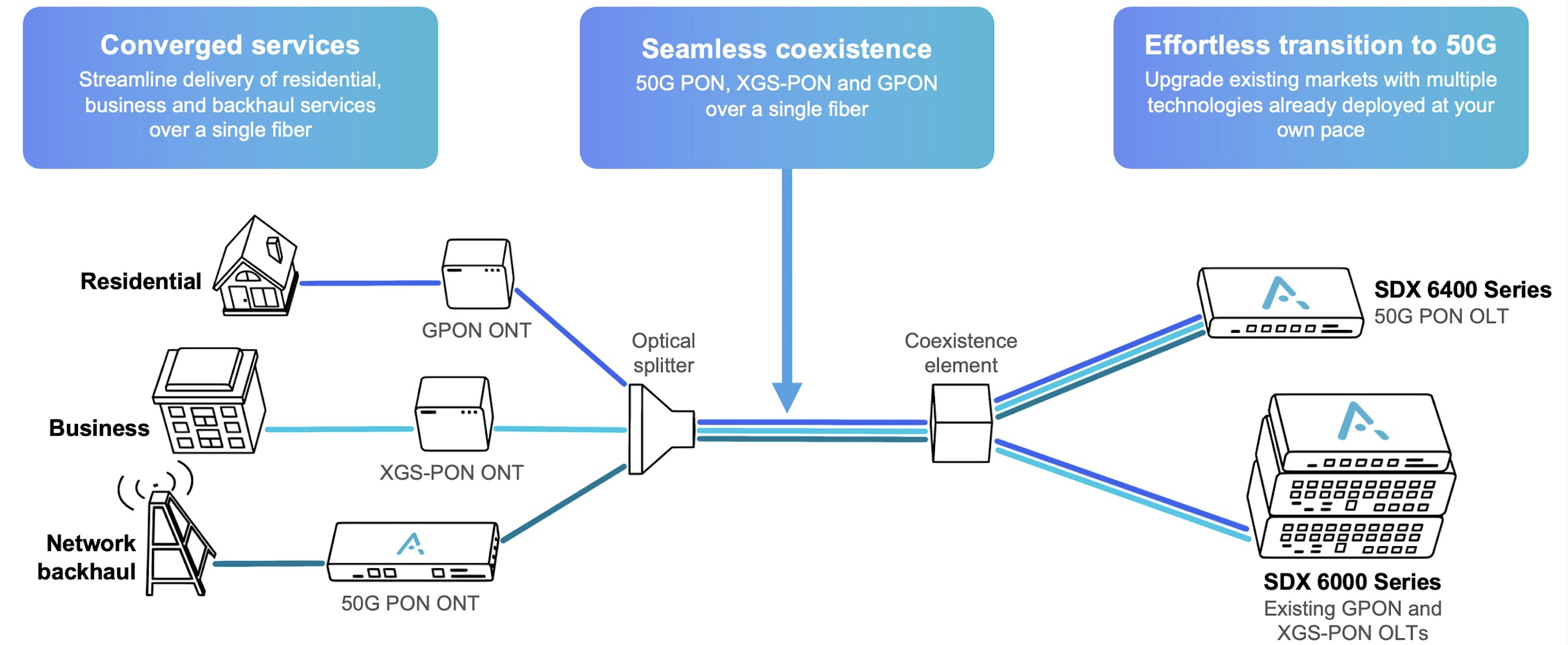
Broadcom has announced two 50G-PON devices: an optical line terminal (OLT) chip and the optical networking unit (ONU) 50-PON port to the users. Both chips include custom hardware from Broadcom to run artificial intelligence (AI) machine-learning algorithms.
Jim Muth, senior manager of product marketing at Broadcom, says supporting AI benefits the operator and the quality of the end user’s broadband service.
High-speed PON
The 50G-PON is the ITU-T’s latest high-speed access standard.
50G-PON follows the organisation’s XGS-PON, a 10-gigabit PON standard, and before that, the original Gigabit PON (GPON) fibre-to-the-home scheme. GPON supports 2.5 gigabit-per-second (Gbps) downstream (to the user) and 1.25Gbps upstream. 50G-PON is backwards compatible with XGS-PON and GPON.

The leading three Chinese operators—China Mobile, China Telecom, and China Unicom—will deploy 50G-PON and have been trialling the technology. Working with Huawei, Orange has undertaken a 50G-PON field trial in Brittany. Meanwhile, European operators such as Altice, BT, Deutsche Telekom, Swisscom, and Telefonica plan to deploy the technology. “It’s too far into the future for them to make a public statement about their activity,” says Muth.
In a separate announcement, Adtran announced that it is working with alternative network (altnet) operator Netomnia to offer 50G-PON services to the UK market. Adtran is using Broadcom’s 50G-PON chips.
Netomnia, after merging with bsk, has the UK’s fourth-largest full-fibre network. Netomnia says adopting 50G-PON will enable it to scale. Its target is to serve one million customers by 2028.
“Many altnets in the US and the UK are interested in 50G-PON technology,” says Stephan Rettenberger, head of marketing and corporate communications at Adtran. “As they’re much smaller than Tier-1 providers, they’re more agile and generally able to deploy new technologies much faster.”
25GS-PON

A competing PON scheme is 25 Gigabit Symmetrical PON (25GS-PON). The 25GS-PON is not a standard but an industry multi-source agreement (MSA) whose members include operators AT&T, Cox Communications, Chunghwa Telecom and equipment makers Nokia, and Ciena. The MSA uses work developed for 25 gigabit Ethernet PON and XGS-PON standards.
Google Fiber offers customers a 20-gigabit connectivity service that includes Wi-Fi 7 that costs $250 a month in select US markets. The high-bandwidth access service uses 25GS-PON.
Adtran favours 50G-PON because it is a standard. “The ITU-standardised generations of PON (GPON, XGS-PON and 50G PON) all co-exist and are the recommended evolutionary steps in the access network,” says Rettenberger.
Applications
Having 50 gigabits of access bandwidth enables other applications besides traditional connectivity services for businesses and residential users. Broadcom cites autonomous driving, where comprehensive cellular coverage is required. For that, many small-cell phone towers are needed along a highway. Instead of each having a backhaul fibre link, several cell towers could share the 50G-PON.
Autonomous driving is some years out, but Muth says infrastructure first needs to be in place. “It’s going to happen over the decade or more, so you have got to start deploying that sooner rather than later,” he says.
Having 50 gigabits of capacity also allows a service provider to offer businesses dedicated bandwidth links, In contrast, XGS-PON is more restricted with its total 10 gigabits of capacity.
Machine learning and PON
The training of AI/ machine-learning algorithms for access is performed by the operator, or by the operator working with a third party. Broadcom says it too works with interested operators.
The training results are weights that are downloaded to its 50G-PON chips to perform inferencing and run the machine-learning algorithms on the operator’s network data. “Most operators are already using AI machine-learning algorithms, but they are running them in the cloud,” says Muth. By adding inferencing hardware on-chip, data remains local to the user and the PON OLT without using precious bandwidth to upload the data for processing in the cloud.
The on-chip AI performs such tasks as intrusion detection and flow classification. Using AI on-chip, intrusion detection can be shut down quicker. Flow classification identifies such traffic as video conferencing, voice calls, and bulk data.
PON hardware has packet processing and traffic management functions, but the issue is that packet headers are increasingly encrypted. Using a machine learning algorithm allows traffic to be identified based on a flow’s nature. “The number of packets over time identifies it,” says Muth. A voice call’s flow has regular if small amounts of data. A video conferencing flow is also regular but has more data. Video traffic can be prioritised ensuring a better experience for the user.
50G-PON chips
Broadcom uses a 7nm CMOS process for the 50G-PON OLT and ONU chips.
The BCM68660 OLT chip integrates what was previously three chips. The chip combines the switch function with packet and traffic processing and two media access controllers (MACs). This allows the chip to support 16 XGS-PON and 16 GPON ports. Each channel supports up to 256 users, but a small split ratio of 1:128 or 1:64 is used in practice. “Now, if you’re going to do 50-gig, it’s a little bit smaller,” says Muth. “It’s eight ports of 50 gig, eight ports of XGS-PON, and eight ports of GPON so that you can do all three simultaneously.”
The chips also support 50-gigabit symmetrical (download and upload), 50Gbps downstream and 25Gbps upstream and 50Gbps downstream and 12.5Gbps upstream. The capacity of the BCM68660 OLT chip totals 500 gigabits.
Having an OLT-on-a-chip reduces power consumption. Muth says the switch chip consumes about 60W, and each PON MAC 15W, for an OLT total of 90W. In contrast, the 7nm CMOS single-chip PON OLT consumes 45-50W.
The ONU BCM 55050 chip is an Ethernet bridge chip. “It terminates the 50-gigabit PON and provides Ethernet to something else, either a switch chip for distribution within a home or a company, or to a gateway chip.”
Meanwhile, Adtran says it is seeing growing interest in the latest PON standard. Now having silicon for a 50G-OLT line card, Adtran can start trialling work. Five customers will trial 50G-PON in the coming months, it says.
ECOC 2024 industry reflections - Part II
Gazettabyte is asking industry figures for their thoughts after attending the recent 50th-anniversary ECOC show in Frankfurt. Here are contributions from Nubis Communications' Dan Harding, imec's Peter Ossieur, and Chris Cole.
Dan Harding, CEO, Nubis Communications
Our biggest takeaway from ECOC is the increased confidence not just in 200-gigabit electrical and optical interfaces but also in 400 gigabit. It is becoming clear that in 2025 and 2026, the industry will broadly launch platforms using a 200 gigabit per lane serdes [serialiser/deserialiser interfaces] that will connect to 200 gigabit per lane optics.
At ECOC, we were shown demonstrations of 400-gigabit serdes. We had several discussions with industry leaders who expressed confidence that serdes can scale to 400 gigabit per lane and that the industry will need optics to support this in the next few years. Different optics approaches were shown at ECOC, but the main takeaway was that serdes speeds continue to advance, and optics needs to figure out a way to keep up.
Our second takeaway is that advancements in materials have significantly reduced loss across printed circuit boards (PCBs), so linear pluggable optics (LPO) at 200 gigabit looks increasingly feasible with vertical line cards and even with traditional ones.
Generally, the 200 gigabit per lane generation will be more similar to the 100-gigabit generation than we thought a year ago. That said, the transition to each new service speed is becoming fuzzy, such that 100 gigabits per lane will have years of overlap with 200 gigabits per lane. The data centre operators and system vendors remain committed to copper for short-reach links, even at 200 gigabit per lane. However, there will be more “active” copper links, so the mix between passive and active copper will shift to more active at 200 gigabit per lane.
As a supplier of optics for AI/ machine-learning networks, the third big takeaway for us is that the speed at which new architectures are being deployed puts an extreme focus on delivering a solution that can quickly move from first samples into volume production. That means we must constantly consider our entire development flow to support this.
Lastly, we were encouraged to see progress on a new form factor for pluggable optics to eliminate the “gold fingers.” This will help the optics industry take advantage of silicon photonics and the density it can deliver. Let’s see how quickly this form factor work progresses, but this is the right direction for the optics industry.
Peter Ossieur, Program Manager, High-Speed Transceivers at imec-IDLab
I noted the speed at which the industry has embraced the concept of linear pluggable optics (LPO). But I’m still unsure how linear pluggable optics will play out.
At ECOC, it was evident that linear pluggable optics are now driving rapid adoption of new materials, notably thin-film lithium niobate. This is excellent news for imec, which is putting significant effort into integrating lithium niobate on its 200mm silicon photonics platform.
As for surprises, one is that co-packaged optics continues to struggle. Another is that the industry’s focus is already turning to 400 gigabit per lane.
Chris Cole, Optical Communications Advisor
The overall ECOC impression was like this year’s OFC show; optics are back with a vengeance. The excitement, buzz, and optimism were infectious. Also uplifting was the focus of the technical conference and the exhibition on solving tough engineering challenges and going after new markets rather than eking out a living. This period may yet be a bubble, but it is a fun ride while it lasts.
There were two important technical trends of note. First, parallelism will become increasingly important, including more fibre and wavelengths. Second, reliability must be approached holistically, and today’s data centre paradigm of swapping failed modules is inadequate to support AI/ machine-learning growth, especially for training.
Also necessary are significantly lower Failures in Time (FIT) for all parts of an optical link, along with system-level redundancy schemes. Achieving this will likely require a shift to fab process-based integration, replacing current discrete assembly methods. This transition is not just a suggestion but a crucial step towards ensuring the reliability and efficiency of optical systems.

ECOC 2024 industry reflections
Gazettabyte is asking industry figures for their thoughts after attending the recent 50th-anniversary ECOC show in Frankfurt. Here are the first contributions from Huawei's Maxim Kuschnerov, Coherent's Vipul Bhatt, and Broadcom's Rajiv Pancholy.
Maxim Kuschnerov, Director R&D, Optical & Quantum Communication Laboratory at Huawei.
At ECOC, my main interest concerned the evolution of data centre networking to 400 gigabits per lane for optics and electronics. Historically, the adoption of new optical line rates always preceded the serdes electrical interconnects but now copper cables are likely to drive much of the leading development work at 400 gigabit per lane.
Arista Networks argued that 448G-PAM6 works better for copper, while 448G-PAM4 is the better choice for optics – a recurring argument. While PAM6 signalling is certainly more suitable for longer copper cables, it will face even tougher challenges on the optical side with increasing reflection requirements in newly built, dusty data centres. Also, a linear drive option for future Ethernet will be imperative, given the DSP’s increasing share of the the consumption in pluggable modules. Here, a native 448G-PAM4 format for the serdes (the attachment unit interface or AUI) and optics looks more practical.
My most important takeaway regarding components was the initial feasibility of electro-absorption modulated lasers (EMLs) with a greater than 100GHz analogue bandwidth, presented by Lumentum and Mitsubishi publicly and other companies privately. Along with thin-film lithium niobate (TFLN) Mach–Zehnder modulators suited for Direct Reach (DR) applications with shared lasers, EMLs have historically offered low cost, small size and native laser integration.
For 1.6-terabit modules, everyone is waiting on the system availability of 224-gigabit serdes at a switch and network interface card (NIC) level. The power consumption of 1.6-terabit optical modules will improve with 3nm CMOS DSPs and native 200 gigabit per lane. Still, it gets into an unhealthy region where the network cable power consumption is in the same ballpark as the system function of switching. Here, the bet on LPO certainly didn’t pay off at 100 gigabits per lane and will not pay off at 200 gigabits per lane at scale. The question is whether linear receive optics (LRO)/ half-retimed approaches will enter the market. Technically, it’s feasible. So, it might take one big market player with enough vertical integration capability and a need to reduce power consumption to move the needle into this more proprietary, closed-system direction. Nvidia showcased their PAM4 DSP at the show. Just saying…
212G VCSELs are still uncertain. There is a tight initial deployment window to be hit if these high-speed VCSELS are to displace single-mode fibre-based optics at the major operators. Coherent’s results of 34GHz bandwidth are not sufficient and don’t look like something that could yet be produced at scale. Claims by some companies that a 400 gigabit per lane VCSEL is feasible sound hollow for now, with the industry crawling around the 30GHz bandwidth window.
Last but not least, co-packaged optics. For years, this technology couldn’t escape gimmick status. Certainly, reliability, serviceability, and testability of co-packaged optics using today’s methodology would make a deployment impractical. However, the big prize at 400 gigabit per lane is saving power – a significant operational expense for operators – something that is too attractive to ignore.
The targets of improving optics diagnostics, developing higher-performance dust-reflection DSP algorithms to deal with multi-path interference, adopting more resiliency to failure in the network, and introducing a higher degree of laser sparing are not insurmountable tasks if the industry sets its mind to them. Given the ludicrous goals of the AI industry, which is reactivating and rebranding nuclear power plants, a significant reduction in network power might finally serve a higher purpose than just building a plumber’s pipe.
Vipul Bhatt, Vice President of Marketing, Datacom Vertical, Coherent
ECOC 2024 was the most convincing testimony that the optical transceiver industry has risen to the challenge of AI’s explosive growth. There was hype, but I saw more solid work than hype. I saw demonstrations and presentations affirming that the 800-gigabit generation was maturing quickly, while preparations are underway for the next leap to 1.6 terabit and then 3.2 terabit.
This is no small feat, because the optics for AI is more demanding in three ways. I call them the three P’s of AI optics: performance, proliferation, and pace.
Performance because 200 gigabit PAM4 optical lanes must work with a low error rate at higher bandwidth. Proliferation because the drive to reduce power consumption has added new transceiver variants like linear packaged optics (LPO) and linear receive optics (LRO). And pace because the specifications of AI optics are evolving at a faster pace than traditional IEEE standards.
Rajiv Pancholy, Director of Hyperscale Strategy and Products, Optical Systems Division, Broadcom
As generative AI systems move to unsupervised, transformer-based parallel architectures, there is less time for resending packets due to data transmission errors. Improved bit error rates are thus required to reduce training times while higher interconnect bandwidth and data rates are needed to support larger GPU clusters. These compute networks are already moving to 224 gigabit PAM4 well before the previous generation at 112 gigabit PAM4 was allowed to reach hyperscale deployment volumes.
The problem is scalability with a high-radix supporting all-to-all connectivity. The power for a single rack of 72 GPUs is 120kW, and even with liquid cooling, this becomes challenging. Interconnecting larger scale-up and scale-out AI computing clusters requires more switching layers which increases latency.
Furthermore, after 224 gigabit PAM4, the losses through copper at 448 gigabit PAM4 make link distances from the ASIC too short. Moving to modulation schemes like PAM-6 or PAM-8 presents a problem for the optics, which would need to stay at 448 gigabit PAM4 to minimize crosstalk and insertion losses.
Supporting 448 gigabit PAM4 with optics then potentially requires new materials to be integrated into silicon, like thin-film lithium niobate (TFLN) and Barium Titanate (BaTiO3), electro-optic (EO) polymers, and III-V materials like Indium Phosphate (InP) and Gallium Arsenide (GaAs). So now we have a gearbox and, potentially, a higher forward error correction (FEC) coding gain is required, adding more power and latency before the signal even gets to the transmit-side optics.
There were 1.6-terabit OSFP transceivers operating with eight lanes of 212.5 gigabit PAM4 while vendors continue to work towards a 3.2-terabit OSFP-XD. With 32 x 3.2Tbps pluggables operating at 40W each, the optical interconnect power would be 1.3kW for a 102.4Tbps switch. And if you use 64 x 1.6Tbps OSFP at 25W each, the optical interconnect power will be eben higher, at 1.6kW. I wonder how linear pluggable optics can compensate for all the path impairments and reflections at high data rates from pluggable solutions. Perhaps you can relax link budgets, temperature requirements, and interoperability compliance.
The best session this year was the last ECOC Market Focus panel on the Tuesday, which kept everyone a bit longer before they could figure out where in Frankfurt Oktoberfest beer was on tap. The panel addressed “Next-Gen Networking Optics like 1.6T or 3.2T”. All but one of the participants discussed the need and a migration to co-packaged optics, which we at Broadcom first demonstrated in March 2022.
It was great to also present at the ECOC Market Focus forum. My presentation was titled “Will you need CPO in 3 years?” Last year in Glasgow, I gave a similar presentation: “Will you need CPO in 5 years?”

Pluggable optics in need of a makeover

Current pluggable optics have stunted optical innovation for the last decade. So argues Chris Cole, industry veteran and an advisor at start-up Quintessent.
Cole calls for a new form factor supporting hundreds of electrical and optical channels. In a workshop on massively parallel optics held at the recent ECOC conference and exhibition in Frankfurt, he outlined other important specifications such a module should have.
Cole, working with other interested parties in the new form factor, will present their proposal to the OIF industry body at its next meeting in November.
“I’m very optimistic it will be approved,” says Cole.
Limitations
Pluggable optics require improvement in several areas.
One limitation is the large, limited number of gold-fingered interconnects on the edge of the printed circuit board (PCB) that fits inside the pluggable module. “This technology goes back 30 or 40 years,” says Cole.
The high-speed OSFP (Octal Small Form-factor Pluggable) module has a row of eight transmit-receive pairs of gold-fingered edge interconnects. The OSFP interface supports 800 gigabits per second (Gbps), and 1.6 terabits per second (Tbps) if 200Gbps signalling is used. The industry can also double capacity to 3.2-terabit with 8x400Gbps signals.
In turn, the QSFP-XD has 16 such pairs arranged in two rows. That promises 3.2Tbps capacity using 16x200Gbps signals and 6.4Tbps with 16x400Gbps signals. However, Cole expects huge signal integrity issues using such a design.
Heat dissipation is another challenge with pluggables. Heat is extracted from a pluggable using a metal plate on the top, which Cole says limits power consumption to 50W.
It is is the low channel count, however, that is the biggest restriction, says Cole.
Meanwhile, yield and reliability have yet to advance. He cites the significant reliability performance achieved by Intel with its integrated laser technology. “It doesn’t do any good because who cares?” he says. “You have a four-channel module, and something’s wrong; you throw it away,” says Cole.
Proposed form factor
The high-capacity form factor proposal calls for a dense, high-bandwidth design. Significant numbers of electrical and optical lanes are needed for that: hundreds rather than eight or 16. Moreover, hundreds of electrical interfaces is not a new concept: Cole cites the large 300-pin MSA used for early embedded coherent modems.
The new form factor would have 2D electrical connections with at least a 0.5mm lower pitch. A high-speed 256-lane count is envisaged, that would also enable many optical lanes and wavelength counts. Each electrical lane should have a bandwidth of 200GHz to support 448Gbps signalling. If implemented, the package’s capacity would be 114Tbps.
“[200GHz lanes] is not very hard to do if you have a connection that is almost negligible height,” says Cole.
Many optical connections are also required, says Cole. He suggests 512, where individual links are supported to ensure a high radix. “We can quibble about the correct number, but it’s not eight or 16,” says Cole. The design should also support liquid cooling to ensure a 100W power consumption.
Optical options
Cole says the design must be optics-agnostic. Nobody can predict the future, he says.
To support 12.8Tbps, for example, it could use 32 optical lanes each at 400Gbps or 16 lanes at 800Gbps both using a thin-film lithium niobate modulator. However, the design should also support many more slower optical channels.
One such 12.8Tbps optical transmission example is 256 channels, each a 50Gbps non-return-to-zero signal, making use of a compact ring-resonator modulators. It could even be 3,200x4Gbps MicroLED channels using an approach favoured by Avicena. It is not out of the question, says Cole.
Cole stresses that while 12.8-terabit and 25.6-terabit capacities may sound high compared to existing pluggable, but the numbers should be viewed as aggregate package capacities. “You would be breaking them out into many channels,” he says.
Retaining features that work
Cole argues that the benefits of pluggable modules must be retained. These include front-plate access, testing, and easy replacement. Equally, the proposed form factor should preserve existing industry business models.
He is also adamant that conventional assembly must be replaced with process-based photonic integration to improve reliability. “The consistency you get in a fab versus what you get in a discrete assembly, there’s an order of magnitude difference there,” he says.
ECOC 2024: AI and Optics
An interview with Gareth Spence of Adtran at the recent ECOC 2024 conference and exhibition

Users embrace OpenLight's silicon photonics platform
OpenLight, the open silicon photonics platform provider, can point to a successful 2024 signing up new customers.
In 2023, OpenLight had three customers bringing photonic integrated circuit (PIC) designs to market. OpenLight has since added 14 more.
OpenLight was formed in 2022 when Juniper Networks carved out its silicon photonics arm. Synopsys acquired a three-quarters stake in OpenLight, while Juniper retained a quarter.
“In the past, the company hadn’t really done any revenue, including when they were in Juniper,” says Adam Carter, OpenLight’s CEO (pictured). “We’ve seen a ten times increase and shown that we can be very profitable.”
The start-up has been creating industry partnerships to better serve its customers’ circuit design, chip manufacturing, and packaging needs.
Silicon photonics foundry partner
Tower Semiconductor was the silicon photonic design team’s chosen foundry long before OpenLight was spun out of Juniper.
Tower now has three dedicated process design kits (PDKs) that take an OpenLight circuit design and run it through the foundry’s wafer manufacturing process line.
The PDKs cover a standard silicon photonics process, one tailored for light detection and ranging (Lidar) applications and one offering distributed feedback (DFB) lasers for artificial intelligence (AI) and high-bandwidth data centre PIC applications.
“You have different specified components in a Lidar process than the data centre one,” says Carter.
For example, the DFB laser requires a diffraction grating to be built into the silicon. The DFBs are used for optical engines supporting coarse wavelength division multiplexing (CWDM) and will support 200-gigabit optical lanes.
OpenLight, working with Riga Technical University and Keysight Technologies, published a post-deadline paper at OFC earlier this year, showing a DFB laser design path for 400-gigabit optical lanes. Future 3.2-terabit transceiver optical engines will need such DFBs.
More partnerships
OpenLight also works using several electronic design automation (EDA) tool environments.
Unsurprisingly, OpenLight works closely with photonic EDA tool specialist Synopsys. “We help them with some of their optical simulation models, and they use us for anything new they’re rolling out,” says Carter.
However, OpenLight also works with other tool vendors to support its customers’ needs and has a partnership with Luceda Photonics, a provider of layout tools.
The start-up has also signed deals with PIC specialists VLC Photonics and Spark Photonics. Since OpenLight has only so many design engineers, it has partnered with the two firms to provide additional design support.
“We have a chip design that we give them, and we ensure their work follows the design rules and guidelines,” says Carter. “Once the design looks good, we sign it off.” The two photonic design firms also develop photonic components for OpenLight to grow its PDK library offerings.
OpenLight has a partnership with manufacturing firm Jabil to provides its customers with services such as assembly, packaging, burn-in, and testing. “As a customer, you take a wafer from Tower, give it to Jabil, and what comes out is a packaged product,” says Carter.
Jabil bought Intel’s optical module unit last year, and Carter says there is an opportunity to supply PICs to that unit, too.
The start-up is also exploring other packaging partners based in Asia to support its customers there.
Lidar opportunities
Two styles of Lidar systems are used for such applications as automotive, autonomous vehicles, and machine vision systems.
One approach, known as time-of-flight, uses VCSELs as the light source. Such systems have limited reach, and the weather can curtail their performance. The second approach is frequency-modulated continuous wave (FMCW) Lidar, which achieves superior range and resolution performance.
But FWCM requires signal amplification, says Carter, something OpenLight can offers with its monolithic process technology that can integrate semiconductor optical amplifiers.
“Much of the work we’re doing with potential Lidar customers is around the fact that we can amplify the signal,” he says.
Carter says time-of-flight systems are the dominant approach for automotive applications in China, but players there are considering alternative architectures. “We are working with Chinese customers on this type of application,” says Carter.
800-gigabit reference designs
OpenLight also offers two 800-gigabit PIC reference designs: an 8×100-gigabit (800G-DR8) design and an 800-gigabit 2xFR4 CWDM one.
The reference designs help OpenLight’s work with sub-assembly companies with their fibre attach units. OpenLight is also using them with its work with electronics suppliers providing PAM-4 (4-level pulse amplitude modulation) digital signal processing (DSP) chips.
“And we are also expanding to an 8×200-gigabit part – a 1.6-terabit DR8, and we’re also doing a [1.6-terabit] CWDM variant,” says Carter. “These will be the first parts to employ the DFB as the laser source.”
At 200 gigabit, the waveguide optical losses are higher. “To meet the specifications, we can add amplification with a semiconductor optical amplifier to boost the output power, compensating for the losses,” he says.
Carter became OpenLight’s CEO at the start of 2023 and is pleased with what the start-up has achieved.
“The team is seeing that what they’ve been working on for several years is becoming a business that can stand on its own,” says Carter.

Ciena sends a 1.6T optical lambda over a 470km link

- Ciena has detailed the first live field trial using its WaveLogic 6 Extreme coherent modem.
- The WaveLogic 6 modem will be generally available from the end of the month.
Ciena’s newest coherent optical modem has sent 1.6 terabits of data over a 470km link. The field trial used Ciena’s WaveLogic 6 Extreme coherent modem in telecom operator Arelion’s live network.
The link connects an Equinix data centre in Ashburn to a Telxius submarine cable landing station, both sites in the state of Virginia.
“The fact that we are achieving 1.6-terabit wavelengths across close to 500 kilometres is a testament to the performance and integrity of the design,” says Helen Xenos, senior director of portfolio marketing at Ciena.
Ciena has won over 20 orders for the WaveLogic 6 Extreme from telecom operators and hyperscalers.
In Ciena’s latest quarterly results, CEO Gary Smith mentioned how Ciena had won business with significant cloud providers covering terrestrial, submarine, and coherent pluggable applications. “The majority [of these are] driven by expected growth in AI and cloud traffic,” said Smith.
WaveLogic 6 Extreme DSP
Ciena announced its WaveLogic 6 Extreme digital signal processor (DSP) early in 2023.
The WaveLogic 6 Extreme is the industry’s first 3nm CMOS process coherent DSP with a maximum symbol rate of 200 gigabaud (GBd). Current leading coherent DSPs deployed use symbol rates ranging from 120-150GBd and support up to 1.2-terabit wavelengths.
The Ciena DSP can execute 1,600 trillion (1.6 x 10¹⁵) operations per second and uses the equivalent of 4km of on-chip copper interconnect.
In contrast, Ciena’s leading deployed DSP device—the WaveLogic 5 Extreme, announced in 2019—is a 7nm CMOS DSP. Over 300 customers have ordered the WaveLogic 5 Extreme.
When it was first announced, the WaveLogic 5 had a baud rate ranging from 60 to 95GBd. Now, its baud rate ranges from 71.0 to 106.9GBd. This highlights how the coherent modem performance has been improved over the years and the same should be expected for the WaveLogic 6 Extreme.
Arelion trial
The Arelion trial is the first Ciena has announced.
“It’s a high bandwidth route connecting a submarine landing station to the data centre capital of the world – Ashburn, Virginia,” says Xenos. “It’s an ideal link to show how WaveLogic 6 can support this massive data volume transmission at today’s fastest speeds.”
The optical wavelength sent 1.6 terabits per second (Tbps) of data over nearly 500 km reach. The WaveLogic 5 Extreme, when first announced, sent 800Gbps some 200km.
“The performance that we can achieve at the highest line rate with WaveLogic 6 is better than what we were able to achieve at the highest line rate with WaveLogic 5 Extreme,” says Xenos. This is because a 3nm CMOS process can cram more digital logic on-chip, enabling the execution of advanced digital signal processing algorithms.
The WaveLogic 6 Extreme improves spectral efficiency by 15 per cent over existing links. The device also delivers 0.25-1 decibel (dB) of signal performance improvement by better tackling nonlinearities introduced by the communication channel during transmission.
The DSP also uses multi-dimensional coding technology to tackle noisy and nonlinear impaired fibre links.
Ciena expects to be able to send 1.6-terabit wavelengths several hundred kilometres over metro networks that feature reconfigurable optical add-drop multiplexers (ROADMs).
The Arelion trial used Ciena’s Waveserver, a two-rack-unit (2RU) optical transport chassis and Ciena’s open 6500 reconfigurable line system (see image below).
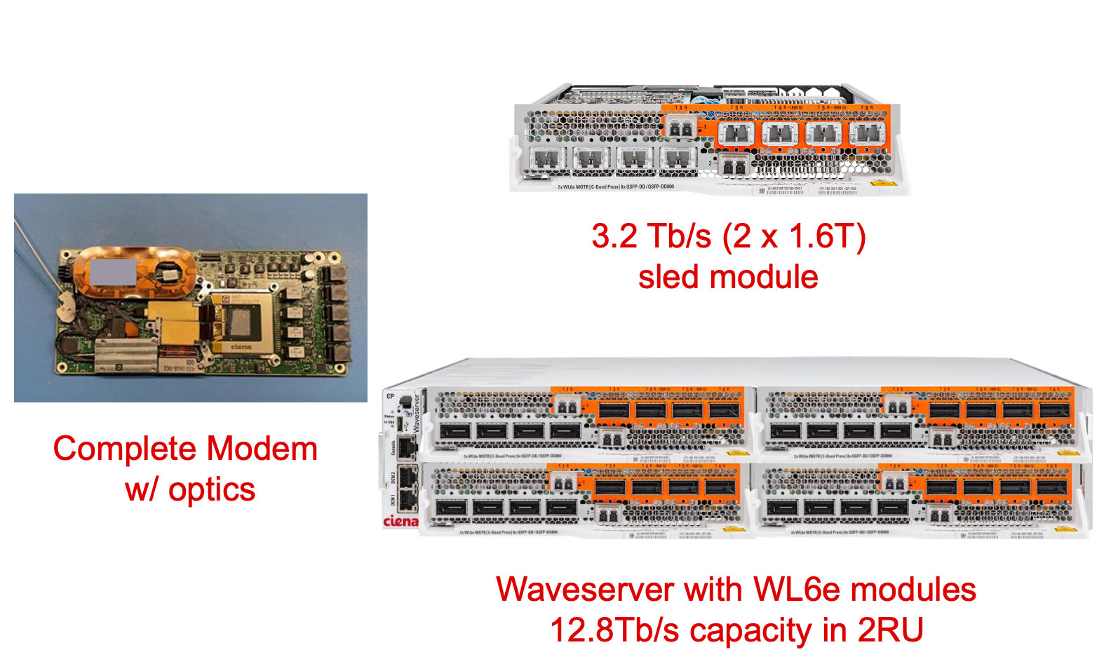
The Waveserver chassis uses insertable sleds, each sled hosting two WaveLogic 6 Extreme coherent modems. Four sleds fit into the Waveserver chassis for a total of eight optical wavelengths and 12.8Tbps transmission capacity.
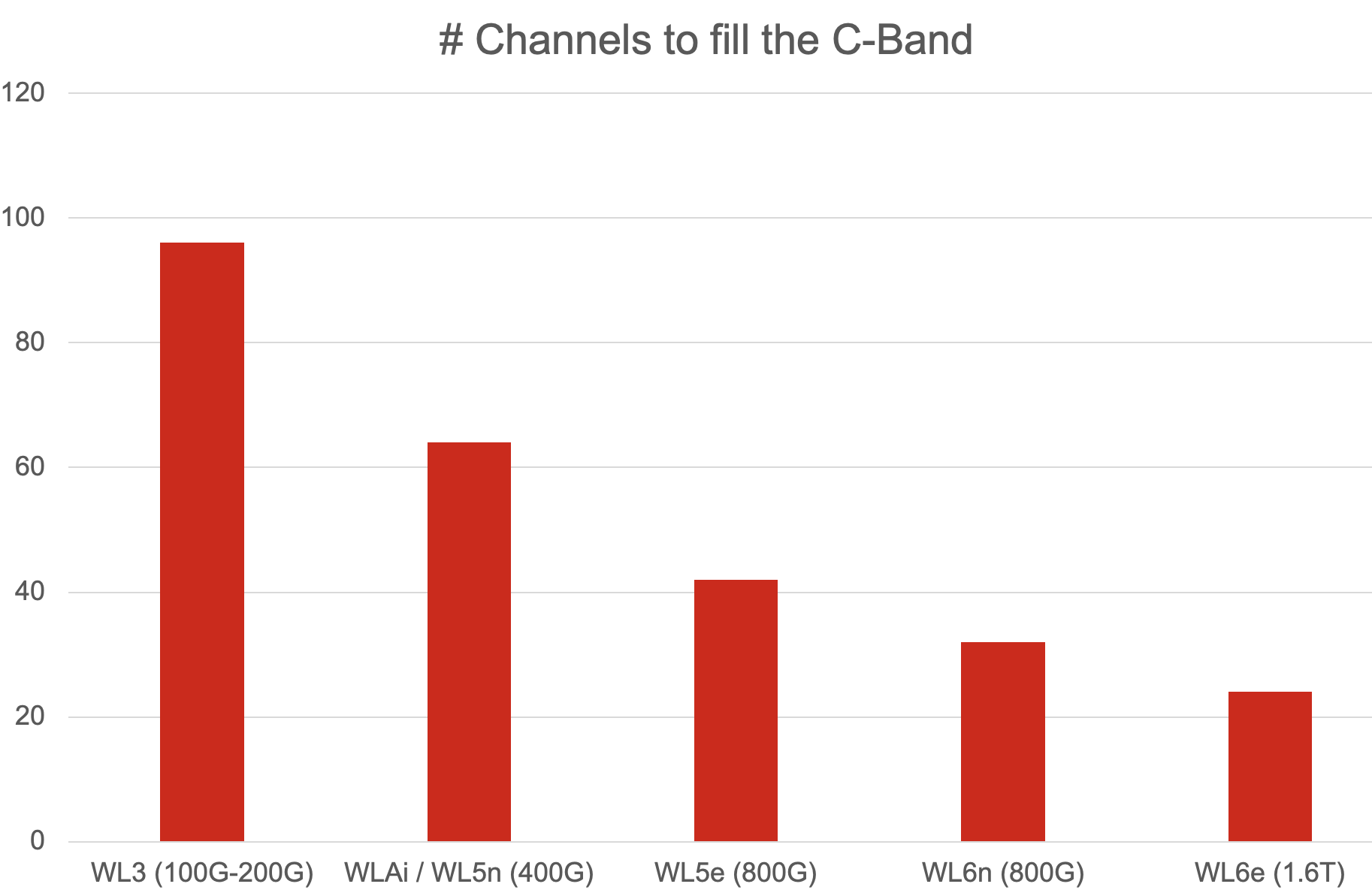
Overall, 24 1.6Tbps wavelengths, each occupying a 200GHz channel, fit into a fibre’s C-band spectrum, giving a total capacity of 38.4Tbps. The same applies to the fibre’s L-band.
“You are filling up the full C-band with only 24 wavelengths,” says Xenos. “It wasn’t that long ago when we filled the C-band with 96, 100-gigabit channels or 64, 400-gigabit channels.” (See chart.)
Ciena says other field trials are planned. Based on its simulation work, Ciena expects its latest coherent modem to send 1.2Tbps across the Atlantic Ocean, 1Tbps across the Pacific Ocean, and 800Gbps over 3,000km. “We expect to see performance improvements because we are still tweaking,” says Xenos.
Embedded and pluggable modules
Coherent pluggable optics continue to advance, especially with the demands of hyperscalers. Coherent pluggable modules, driven by hyperscalers’ data centre interconnect demands, also continue to advance. So, is the requirement for the highest-performance embedded modules diminishing?
Ciena believes that both classes of devices are needed: performance-optimised (embedded) and pluggable coherent optical modules.
“There are more capabilities that are becoming available in pluggables, with the 800-gigabit generation extending to 1,000km and beyond and with L-band offerings coming in the near future,” she says. “If you can integrate the pluggable into a router platform, that allows you to save on space and power.”
However, the pluggable can’t match the spectral efficiency of an embedded coherent module. An 800-gigabit pluggable uses a 150GHz channel spacing, which is the same spectral efficiency as the earlier generation Ciena WaveLogic AI.
The latest embedded modules, in contrast, can be significantly better than equivalent line reate pluggables: from 1.3x to 2x. This is an important consideration in environments where fibre is scarce.
Another point Xenos makes is the nature of the optical network and its total cost, not just the optics (embedded or pluggable) but also the optical line system. If a link has many amplification stages and ROADMs, the optical line makes a more significant contribution to the overall cost. Here embedded optics is needed to span the more complex optical route while being one part of the overall cost.
“You have to look at the total overall cost of building the network,” says Xenos. “It is the optics and the photonic line system.”
General availability
The WaveLogic 6 Extreme will be generally available at the end of September 2024.
When Ciena first announced the coherent DSP, the company expected the device to be generally available in the first half of 2024. In March at OFC 2024, Ciena gave an update saying trials would start this summer.
Xenos says the delivery date did slip by several months. But she stresses the achievement of delivering such a complex coherent modem system. As well as designing the chip in a 3nm CMOS process, the DSP also includes very high-speed mixed-signal analogue-to-digital and digital-to-analogue converters.
“When you target a certain availability, it is the best date that is also realistic,” says Xenos. “The fact that we’re only a few months off means that the team has executed to deliver a working product.”
Ciena is also integrating WaveLogic 6 into its 6500 optical transport platform and will make a coherent WaveLogic 6 module available for OEMs or developers that have custom equipment requirements.
Meanwhile, Ciena continues to develop the Nano, the second WaveLogic 6 device designed for the coherent pluggable market. The WaveLogic 6 Nano is expected to be sampled at the end of the year.
Market consolidation
In June, Nokia announced its intention to acquire Infinera. If the deal passes regulatory approval, it will reduce the number of companies capable of developing high-end coherent DSPs.
More players mean greater competition which pushes the marketplace. But developing coherent DSPs using shrinking CMOS nodes is getting more expensive. One fewer player can be viewed as good news for the rest. Xenos says Ciena has expected fewer high-end coherent players going forward.
“Those who are vertically integrated have an advantage of improved cost efficiencies that they can offer to their end-customers,” she says. “And we’ve been investing in vertical integration because it allows us to control our destiny and come to market with new technology at an earlier time.”
This is what the company has done with the WaveLogic 6 Extreme, where Ciena had to develop its own 100GHz analogue bandwidth coherent optics to achieve the 200GBd symbol rate.
Future developments
The roadmap for coherent pluggable modules is well defined due to the industry organisation, the OIF’s 1600ZR and 1600ZR+ 1.6Tbps coherent pluggable modules which are expected from 2028. For embedded modules the roadmap is less clear.
“There is nothing to announce at this time, but we know that the next step has to be bold enough to provide a meaningful benefit for its adoption into the network,” says Xenos.