
Verizon readies its metro for next-generation P-OTS
Verizon is preparing its metro network to carry significant amounts of 100 Gigabit traffic and has detailed its next-generation packet-optical transport system (P-OTS) requirements. The operator says technological advances in 100 Gig transmission and new P-OTS platforms - some yet to be announced - will help bring large scale 100 Gig deployments in the metro in the next year or so.
 Glenn Wellbrock
The operator says P-OTS will be used for its metro and regional networks for spans of 400-600km. "That is where we have very dense networks," says Glenn Wellbrock, director of optical transport network architecture and design at Verizon. "The amount of 100 Gig is going to be substantially higher than it was in long haul."
Verizon announced in April that it had selected Fujitsu and Coriant for a 100 Gig metro upgrade. The operator has already deployed Fujitsu's FlashWave 9500 and the Coriant 7100 (formerly Tellabs 7100) P-OTS platforms. "The announcement [in April] is to put 100 Gig channels in that embedded base," says Wellbrock.
The operator has 4,000 reconfigurable optical add/ drop multiplexers (ROADMs) across its metro networks worldwide and all support 100 Gig channels. But the networks are not tailored for high-speed transmission and hence the cost of 100 Gig remains high. For example, dispersion compensation fibre, and Erbium-doped fibre amplifiers (EDFA) rather than hybrid EDFA-Raman are used for the existing links. "It [the network] is not optimised for 100 Gig but will support it, and we are using [100 Gig] on an as-needed basis," says Wellbrock.
The metro platform will be similar to those used for Verizon's 100 Gig long-haul in that it will be coherent-based and use advanced, colourless, directionless, contentionless and flexible-grid ROADMs. "But all in a package that fits in the metro, with a much lower cost, better density and not such a long reach," says Wellbrock.
The amount of 100 Gig is going to be substantially higher than it was in long haul
One development that will reduce system cost is the advent of the CFP2-based line-side optical module; another is the emergence of third- or fourth-generation coherent DSP-ASICs. "We are getting to the point where we feel it is ready for the metro," says Wellbrock. "Can we get it to be cost-competitive? We feel that a lot of the platforms are coming along."
The latest P-OTS platforms feature enhanced packet capabilities, supporting carrier Ethernet, multi-protocol label switching - transport profile (MPLS-TP), and high-capacity packet and Optical Transport Network (OTN) switching. Recently announced P-OTS platforms suited to Verizon's metro request-for-proposal include Cisco Systems' Network Convergence System (NCS) 4000 and Coriant's mTera. Verizon says it expects other vendors to introduce platforms in the next year.
Verizon still has over 250,000 SONET elements in its network. Many are small and reside in the access network but SONET also exists in its metro and regional networks. The operator is keen to replace the legacy technology but with such a huge number of installed network elements, this will not happen overnight.
Verizon's strategy is to terminate the aggregated SONET traffic at its edge central offices so that it only has to deal with large Ethernet and OTN flows at the network node. "We plan to terminate the SONET, peel out the packets and send them in a packet-optimised fashion," says Wellbrock. In effect, SONET is to be stopped from an infrastructure point of view, he says, by converting the traffic for transport over OTN and Ethernet.
SDN and multi-layer optimisation
The P-OTS platform, with its integrated functionality spanning layer-0 to layer-2, will have a role in multi-layer optimisation. The goal of multi-layer optimisation is to transport services on the most suitable networking layer, typically the lowest, most economical layer possible. Software-defined networking (SDN) will be used to oversee such multi-layer optimisation.
However, P-OTS, unlike servers used in the data centre, are specialist rather than generic platforms. "Optical stuff is not generic hardware," says Wellbrock. Each P-OTS platform is vendor-proprietary. What can be done, he says, is to use 'domain controllers'. Each vendor's platform will have its own domain controller, above which will sit the SDN controller. Using this arrangement, the vendor's own portion of the network can be operated generically by an SDN controller, while benefitting from the particular attributes of each vendor's platform using the domain controller.
There is always frustration; we always want to move faster than things are coming about
Verizon's view is that there will be a hierarchy of domain and SDN controllers."We assume there are going to be multiple layers of abstraction for SDN," says Wellbrock. There will be no one, overriding controller with knowledge of all the networking layers: from layer-0 to layer-3. Even layer-0 - the optical layer - has become dynamic with the addition of colourless, directionless, contentionless and flexible-grid ROADM features, says Wellbrock.
Instead, as part of these abstraction layers, there will be one domain that will control all the transport, and another that is all-IP. Some software element above these controllers will then inform the optical and IP domains how best to implement service tasks such as interconnecting two data centres, for example. The transport controller will then inform each layer its particular task. "Now I want layer-0 to do that, and that is my Ciena box; I need layer-1 to do this and that happens to be a Cyan box; and we need MPLS transport to do this, and that could be Juniper," says Wellbrock, pointing out that in this example, three vendor-domains are involved, each with its own domain controller.
Is Verizon happy with the SDN progress being made by the P-OTS vendors?
"There is always frustration; we always want to move faster than things are coming about," says Wellbrock. "The issue, though, is that there is nothing I see that is a showstopper."
The art of virtualised network function placement
Cyan is delivering its Blue Planet NFV orchestrator software that will make use of enhancements being made to OpenStack developed by Red Hat in close collaboration with Telefónica.
Gazettabyte asked Nirav Modi, director of software innovations at Cyan, about the work.
Q: The concept of deterministic placement of virtualised network functions. Why is this important?
NM: We are attempting to solve a fundamental technology challenge required to make NFV successful for carriers. Telefónica has been doing a lot of internal trials and its own NFV R&D and has found that the placement of virtualised network functions greatly affects their performance.
We are working with Telefónica and Red Hat to solve this problem, to ensures virtualised network functions perform consistently and at their peak from one instance to another. This is particularly important for composite or clustered virtualised network function architectures, where the placement of various components can affect performance and availability.
Also, you need to ensure that the virtualised network functions are located where the most suitable compute, storage or networking resources are located. Other important performance metrics that need to be considered include latency and bandwidth availability into the cloud environment.
What is involved in enabling deterministic virtualised network functions, and what is the impact on Cyan's orchestration platform?
Deterministic placement requires an orchestration platform, such as Cyan’s Blue Planet, to be aware of the resources available at various NFV points of presence (PoPs) and to map operator-provided placement policies, such as performance and high-availability requirements, into placement decisions. In other words, which servers should be used and which PoP should host the virtualised network function.
For the operator, interested in application service-level agreements (SLAs) and performance, Cyan’s orchestration platform provides the intelligence to translate those policies into a placement architecture.
Does this Telefonica work also require Cyan's Z-Series packet-optical transport system (P-OTS)?
NFV is all about taking network functions currently deployed on purpose-built, vertically-integrated hardware platforms, and deploying them on industry-standard commercial off-the-shelf (COTS) servers, possibly in a virtualised environment running OpenStack, for example.
In such an set-up, Cyan’s Blue Planet orchestration platform is responsible for the deployment of the virtualised network functions into the NFV infrastructure or telco cloud. Cyan’s orchestration software is always deployed on COTS servers. There is no dependency on using Cyan’s P-OTS to use the Blue Planet software-defined networking (SDN) and NFV software.
The Z-Series platform can be used in the metro and wide area network to enable a scalable and programmable network. And this can supplement the virtual network functions deployed in the cloud to replace existing hardware-based solutions, but the Z-Series is not involved in this joint-effort with Telefónica and Red Hat.
NFV moves from the lab to the network
 Dor Skuler
In October 2012, several of the world's leading telecom operators published a document to spur industry action. Entitled Network Functions Virtualisation - Introductory White Paper, the document stressed the many benefits such a telecom transformation would bring: reduced equipment costs, power consumption savings, portable applications, and nimbleness instead of ordeal when a service is launched.
Eighteen months on and much progress has been made. Operators and vendors have been identifying the networking functions to virtualise on servers, and the impact Network Functions Virtualisation (NFV) will have on the network.
A group within ETSI, the standards body behind NFV, is fleshing out the architectural layers of NFV: the virtual network functions layer that resides above the management and orchestration one that oversees the servers, distributed in data centres across the network.
In the lab, network functions have been put on servers and then onto servers in the cloud. "Now we are at the start of the execution phase: leaving the lab and moving into first deployments in the network," says Dor Skuler, vice president and general manager of CloudBand, the NFV spin-in of Alcatel-Lucent. Skuler views 2014 as the year of experimentation for NFV. By 2015, there will be pockets of deployments but none at scale; that will start in 2016.
SDN is a simple way for virtual network functions to get what they need from the network through different commands
Deploying NFV in the network and at scale will require software-defined networking (SDN). That is because network functions make unique requirements of the network, says Skuler. Because the network functions are distributed, each application must make connections to the different sites on demand. "SDN is a simple way for virtual network functions to get what they need from the network through different commands," he says.
CloudBand's customers include Deutsche Telekom, Telefonica and NTT. Overall, the company says it is involved in 14 customer projects.
CloudBand 2.0
CloudBand has developed a management and orchestration platform, and launched an 'ecosystem' that includes 25 companies. Companies such as Radware and Metaswitch Networks are developing virtual network functions that use the CloudBand platform.
More recently, CloudBand has upgraded its platform, what it calls CloudBand 2.0, and has launched its own virtualised network functions (VNFs) for the Long Term Evolution (LTE) cellular standard. In particular, VNFs for the Evolved Packet Core (EPC), IP Multimedia Subsystem (IMS) and the radio access network (RAN). "These are now virtualised and running in the cloud," says Skuler.
SDN technology from Nuage Networks, another Alcatel-Lucent spin-in, has been integrated into the CloudBand node that is set up in a data centre. The platform also has enhanced management systems. "How to manage the many nodes into a single logical cloud, with a lot of tools that help applications," says Skuler. CloudBand 2.0 has also added support for OpenStack alongside its existing support for CloudStack. OpenStack and CloudStack are open-source platforms supporting cloud.
For the EPC, the functions virtualised are on the network side of the basestation: the Mobility Management Entity (MME), the Serving Gateway and Packet Data Network Gateway (S- and P-Gateways) and the Policy and Charging Rules Function (PCRF).
IMS is used for Voice over LTE (VoLTE). "Operators are looking for more efficient ways of delivering VoLTE," says Skuler. This includes reducing deployment times and scalability, growing the service as more users sign up.
The high-frequency parts of the radio access network, typically located in a remote radio head (RRH), cannot be virtualised. What can is the baseband processing unit (BBU). The BBUs run on off-the-shelf servers in pools up to 40km away from the radio heads. "This allows more flexible capacity allocation to different radio heads and easier scaling and upgrading," says Skuler.
Skuler points out that virtualising a function is not simply a case of putting a piece of code on a server running a platform such as CloudBand. "The VNF itself needs to go through a lot of change; a big monolithic application needs to be broken up into small components," he says.
"The VNF needs to use the development tools we offer in CloudBand so it can give rules so it can run in the cloud." The VNF also needs to know what key performance indicators to look at, and be able to request scaling, and inform the system when it is unhealthy and how to remedy the situation.
These LTE VNFs are designed to run on CloudBand and on other vendors' platforms. "CloudBand won't be run everywhere which is why we use open standards," says Skuler.
Pros and cons
The benefits from adopting NFV include prompt service deployment, "Today it can take 9-18 months for an operator to scale [a service]," says Skuler. The services, effectively software on servers, can scale more easily whereas today, typically, operators have to overprovision to ensure extra capacity is in place.
Less equipment also needs to be kept by operators for maintainance. "A typical North America mobile operator may have 450,000 spare parts," says Skuler; items such as line cards and power supplies. With automation and the use of dedicated servers, the number of spare parts held is typically reduced by a factor of ten.
Services can be scaled and healed, while functionality can be upgraded using software alone. "If I have a new verison of IMS, I can test it in parallel and then migrate users; all behind my desk at the push of a button," says Skuler.
The NFV infrastructure - comprising compute, storage, and networking resources - reside at multiple locations - the operator's points-of-presence. These resources are designed to be shared by applications - VNFs - and it is this sharing of a common pool of resources that is one of the biggest advantages of NFV, says Skuler.
But there are challenges.
"Operating [existing] systems has been relatively simple; if there is a faulty line card, you simply replace it," says Skuler. "Now you have all these virtual functions sitting on virtual machines across data centres and that creates complexities."
An application needs to be aware of this and provide the required rules to the management and orchestration system such as CloudBand. Such systems need to provide the necessary operational tools to operators to enable automated upgrades and automated scaling as well as pinpoint causes of failures.
For example, an IMS core might have 12 tiers. In cloud-speak, a tier is one of a set of virtual machines making up a virtual network function. Examples of a tier include a load balancer, an application or a database server. Each tier consists of one or more virtual machines. Scaling of capacity is enabled by adding or removing virtual machines from a tier.
In a cloud deployment, these linkages between tiers must be understood by the system to allow scaling. Two tiers may be placed in the same data centre to ensure low latency, but an extra pair of the tier-pair may be placed in separate sites in case one pair goes down. SDN is used to connect the different sites, says Skuler: "All this needs to be explained simply to the system so that it understands it and execute it".
That, he says, is what CloudBand does.
See also:
Telcos eye servers and software to meet networking needs, click here
Netronome prepares cards for SDN acceleration
 Source: Netronome
Netronome has unveiled 40 and 100 Gigabit Ethernet network interface cards (NICs) to accelerate data-plane tasks of software-defined networks.
Dubbed FlowNICs, the cards use Netronome's flagship NFP-6xxx network processor (NPU) and support open-source data centre technologies such as the OpenFlow protocol, the Open vSwitch virtual switch, and the OpenStack cloud computing platform.
Four FlowNIC cards have been announced with throughputs of 2x40 Gigabit Ethernet (GbE), 4 x 40GbE, 1 x 100GbE and 2 x 100GbE. The NICs use either two or four PCI Express 3.0 x8 lane interfaces to achieve the 100GbE and 200GbE throughputs.
"We are the first to provide these interface densities on an intelligent network interface card, built for SDN use-cases," says Robert Truesdell, product manager, software at Netronome. "We have taken everything that has been done in Open vSwitch that would traditionally run on an [Intel] x86-based server, and run it on our NFP-6xxx-based FlowNICs at a much faster rate."
The cards have accompanying software that supports OpenFlow and Open vSwitch. There are also two additional software packages: cloud services, which performs such tasks as implementing the tunnelling protocols used for network virtualisation, and cyber-security.
Implementing the switch and packet processing functions on a FlowNIC card instead of using a virtual switch frees up valuable computation resources on a server's CPUs, enabling data centre operators to better use their servers for revenue-generating tasks. "They are trying to extract the maximum revenue out of the server and that is what this buys," says Truesdell.
Designing the FlowNICs around a programable network processor has other advantages. "As standards evolve, that allows us to do a software revision rather than rely on a hardware or silicon revision," says Truesdell. The OpenFlow specification, for example, is revised every 6-12 months, he says, the most recent release being V1.4.
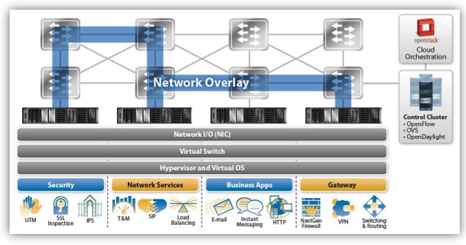
In the data centre, software-defined networking (SDN) uses a central controller to oversee the network connecting the servers. A server's NIC provides networking input/ output, while the server runs the software-based virtualised switch and the hypervisor that supports virtual machines and operating systems on which the applications run. Applications include security tasks such as SSL inspection, intrusion detection and intrusion prevention systems; load balancing; business applications like email, the hypertext transfer protocol and instant messaging; and gateway functions such as firewalls and virtual priviate networks (VPNs).
We have taken everything that has been done in Open vSwitch that would traditionally run on an x86-based server, and run it on our NFP-6xxx-based FlowNICs at a much faster rate
With Open vSwitch running on a server, the SDN protocols such as OpenFlow pass communications between the data plane device - either the softswitch or the FlowNIC - and the controller. "By supporting Open vSwitch and OpenFlow, it allows us to inherit compatibility with the [SDN] controller and orchestration layers," says Truesdell. The FlowNIC is compatible with controllers from OpenDaylight, Ryu and VMWare's NFX network virtualisation system, as well as orchestration platforms like OpenStack.
The virtual switch performs two main tasks. It inspects packet headers and passes the traffic to the appropriate virtual machines. The virtual switch also implements network virtualisation: setting up network overlays between servers for virtual machines to talk to each other.
Packet encapsulation and unwrapping performance required for network virtualisation tops out when implemented using the virtual switch, such that the throughput suffers. Moreover, packet header inspections can be nested if, for example, encryption and network virtualisation are used, further impacting performance. "The throughput rates can really suffer on a server because it is not optimised for this type of workload," says Truesdell.
Performing the tasks using the FlowNIC's network processor enables packet processing to keep up with the line rate including for the most demanding, shortest packet sizes. The issue with packet size is that the shorter the packet (the smaller the data payload), the more frequent the header inspections. "Data centre traffic is very bursty," says Truesdell. "These are not long-lived flows - they have high connection rates - and this drives the packet sizes down."
For a 10 Gigabit stream performing the Network Virtualization using Generic Routing Encapsulation (NVGRE) protocol, the forwarding throughput is at line rate for all packet sizes using the company's existing FlowNIC acceleration cards, based on its previous generation NFP-3240 network processor.
In contrast, NVGRE performance using Open vSwitch on the server is at 9Gbps for lengthy 1,500-byte packets and drops continually to 0.5Gbps for 64-byte packets. The average packet length is around 400 bytes, says Truesdell.
Overall, Netronome claims that using its FlowNICs, virtualised networking functions and server applications are boosted by over twentyfold compared to using the virtual switch on the server's CPU.
Netronome's FlowNIC-32xx cards are already used by one Tier 1 operator to perform gateway functions. The gateway, overseen using a Ryu controller running OpenFlow, translates between multi-tenant IP virtual LANs in the data centre and MPLS-based VPNs that connect the operator's enterprise customers.
The NFP-6xxx-based FlowNICs will be available for early access partners later this quarter. FlowNIC customers include data centre equipment makers, original design manufacturers and the largest content service providers - the 'internet juggernauts' - that operate hyper-scale data centres.
For an article written for Fibre Systems on network virtualisation and data centre trends, click here
OFDM promises compact Terabit transceivers
 Source ECI Telecom
A one Terabit super-channel, crafted using orthogonal frequency-division multiplexing (OFDM), has been transmitted over a live network in Germany. The OFDM demonstration is the outcome of a three-year project conducted by the Tera Santa Consortium comprising Israeli companies and universities.
Current 100 Gig coherent networks use a single carrier for the optical transmission whereas OFDM imprints the transmitted data across multiple sub-carriers. OFDM is already used as a radio access technology, the Long Term Evolution (LTE) cellular standard being one example.
With OFDM, the sub-carriers are tightly packed with a spacing chosen to minimise the interference at the receiver. OFDM is being researched for optical transmission as it promises robustness to channel impairments as well as implementation benefits, especially as systems move to Terabit speeds.
"It is clear that the market has voted for single-carrier transmission for 400 Gig," says Shai Stein, chairman of the Tera Santa Consortium and CTO of system vendor, ECI Telecom. "But at higher rates, such as 1 Terabit, the challenge will be to achieve compact, low-power transceivers."

The real contribution [of OFDM] is implementation efficiency
Shai Stein
One finding of the project is that the OFDM optical performance matches that of traditional coherent transmission but that the digital signal processing required is halved. "The real contribution [of OFDM] is implementation efficiency," says Stein.
For the trial, the 175GHz-wide 1 Terabit super-channel signal was transmitted through several reconfigurable optical add/drop multiplexer (ROADM) stages. The 175GHz spectrum comprises seven, 25GHz bands. Two OFDM schemes were trialled: 128 sub-carriers and 1024 sub-carriers across each band.
To achieve 1 Terabit, the net data rate per band was 142 Gigabit-per-second (Gbps). Adding the overhead bits for forward error corrections and pilot signals, the gross data rate per band is closer to 200Gbps.
The 128 or 1024 sub-carriers per band are modulated using either quadrature phase-shift keying (QPSK) or 16-quadrature amplitude modulation (16-QAM). One modulation scheme - QPSK or 16-QAM - was used across a band, although Stein points out that the modulation scheme can be chosen on a sub-carrier by sub-carrier basis, depending on the transmission conditions.
The trial took place at the Technische Universität Dresden, using the Deutsches Forschungsnetz e.V. X-WiN research network. The signal recovery was achieved offline using MATLAB computational software. "It [the trial] was in real conditions, just the processing was performed offline," says Stein. The MATLAB algorithms will be captured in FPGA silicon and added to the transciever in the coming months.
Using a purpose-built simulator, the Tera Santa Consortium compared the OFDM results with traditional coherent super-channel transmission. "Both exhibited the same performance," says David Dahan, senior research engineer for optics at ECI Telecom. "You get a 1,000km reach without a problem." And with hybrid EDFA-Raman amplification, 2,000km is possible. The system also demonstrated robustness to chromatic dispersion. Using 1024 sub-carriers, the chromatic dispersion is sufficient low that no compensation is needed, says ECI.
Stein says the project has been hugely beneficial to the Israeli optical industry: "There has been silicon photonics, transceiver and algorithmic developments, and benefits at the networking level." For ECI, it is important that there is a healthy local optical supply chain. "The giants have that in-house, we do not," says Stein.
One Terabit transmission will be realised in the marketplace in the next two years. Due to the project, the consortium companies are now well placed to understand the requirements, says Stein.
Set up in 2011, the Tera Santa Consortium includes ECI Telecom, Finisar, MultiPhy, Cello, Civcom, Bezeq International, the Technion Israel Institute of Technology, Ben-Gurion University, and the Hebrew University in Jerusalem, Bar-Ilan University and Tel-Aviv University.
X-Celeprint brings printing technology to silicon photonics
 X-Celeprint's micro transfer printing technology. Source: X-Celeprint
- X-Celeprint has a printing process that places individual 'chiplets' of III-V material onto silicon
- The micro transfer printing technique can be used to make silicon photonics circuits
- X-Celeprint will work with silicon photonics companies interested in licensing its technology
A key challenge facing silicon photonics players is creating a light source. Silicon does not lase so a III-V material is needed to form the laser.
One approach is to attach a tiny module holding the laser to the silicon photonics design. This is what the likes of Cisco Systems, Luxtera, Mellanox Technologies and IBM are doing: adding an external laser to the otherwise monolithic silicon photonics circuit.
An alternative technique is to bond the III-V material to the silicon and using photolithography and etching to construct the silicon photonics device. The attraction of III-V bonding is that the technique can be used to also make the modulators and photo-detectors. Known as heterogeneous integration, this approach is being used by companies such as Aurrion, Intel and Skorpios Technologies.
"Bonding is an elegant solution," says Roel Baets, a professor at the Photonics Research Group at Ghent University. "You can make the light source at the wafer scale and have a single chip solution that looks like a monolithic chip, including the light source."
Think of printing as pick-and-place in a massively parallel fashion. Instead of ink, we are picking up and printing arrays of high-performance semiconductors.
Bonding III-V material to silicon is itself non-trivial. First, silicon wafers are either 200mm or 300mm (8 or 12 inch) while III-V indium phosphide wafers are typically 50mm (2 inch). Indium phosphide wafers are also expensive, simply etching away the majority of the wafer to leave small islands of wanted material is hugely wasteful.
"There is only going to be a laser here or there, with a fill factor - an area coverage - of some one percent," says Baets. "You are throwing away a lot of III-V."
Equally, cutting up the III-V wafer into small slivers for bonding is complicated as it requires precision placement; a process difficult to automate to achieve high-yield circuits. This is the challenge the heterogeneous integration companies have set themselves.
It is a market opportunity identified by start-up X-Celeprint. It has a process that places individual 'chiplets' of III-V material onto silicon by the thousands.
X-Celeprint uses a micro transfer printing to place the chiplets onto silicon. "Think of printing as pick-and-place in a massively parallel fashion," says Kyle Benkendorfer, CEO of X-Celeprint. "Instead of ink, we are picking up and printing arrays of high-performance semiconductors."
Micro transfer printing is already used commercially to make high concentration solar cells, and it is being evaluated to place thin lasers on read/ write heads in disc drives. "We can print live devices or a slab of material on any substrate as long as it is flat," says Benkendorfer.
One benefit of the technique is that the thin III-V material is removed from the indium phosphide wafer but the underlying substrate is retained and can be recycled. For wafer-to-wafer bonding, in contrast, the substrate must be ground back. "This is several hundred microns of [substrate] material," says Benkendorfer. "With our process you can reprocess the wafer and regrow it, saving some $3,000."
The printing process also lends itself to automation. "We can very efficiently place active die of highly expensive compound material at the point of use, where it can then be converted into a device," he says.
X-Celeprint wants to work with silicon photonics companies interested in licensing its printing technology. Developing the process with a particular silicon photonics vendor takes time. Each application requires tailoring and it can take up to two years to make, test and scale up production, says the start-up.
"We recognise that silicon photonics as a large market is out there, no question," says Benkendorfer. "But the development time to get any significant market is going to be a while."
MultiPhy eyeing 400 Gig after completing funding round
MultiPhy is developing a next-generation chip design to support 100 and 400 Gigabit direct-detection optical transmission. The start-up raised a new round of funding in 2013 but has neither disclosed the amount raised nor the backers except to say it includes venture capitalists and a 'strategic investor'.
The start-up is already selling its 100 Gig multiplexer and receiver chips to system vendors and module makers. The devices are being used for up to 80km point-to-point links and dense WDM metro/ regional networks spanning hundreds of kilometers. "In every engagement we have, the solutions are being sold in both data centre and telecom environments," says Avi Shabtai, CEO of MultiPhy.
The industry has settled on coherent technology for long-distance 100 Gig optical transmission but coherent is not necessarily a best fit for certain markets if such factors as power consumption, cost and compatibility with existing 10 Gig links are considered, says Shabtai.
The requirement to connect geographically-dispersed data centres has created a market for 100 Gig direct-detection technology. The types of data centre players include content service providers, financial institution such as banks, and large enterprises that may operate their own networks.
In every engagement we have, the solutions are being sold in both data centre and telecom environments
MultiPhy's two chips are the MP1101Q, a 4x25 Gig multiplexer device, and the MP1100Q four-channel receiver IC that includes a digital signal processor implementing the MLSE algorithm.
The chipset enables 10 Gig opto-electronics to be used to implement the 25 Gig transmitter and receiver channels. This results in a cost advantage compared to other 4x25 Gig designs. A design using the chipset can achieve 100 Gig transmissions over a 200GHz-wide channel or a more spectrally efficient 100GHz one. The latter achieves a transmission capacity of 4 Terabits over a fibre.
ADVA Optical Networking is one system vendor offering 100 Gig direct-detection technology while Finisar and Oplink Communications are making 100 Gigabit direct-detection optical modules. Oplink announced that it is using MultiPhy's chipset in 2013.
Overall, at least four system vendors are in advanced stages of developing 100 Gig direct-detection, and not all will necessarily announce their designs, says Shabtai. Whereas all the main optical transmission vendors have 100 Gig coherent technology, those backing 100 Gig direct detection may remain silent so as not to tip off their competitors, he says.
We assume we can do more using those [25 Gig] optical components with our technology
Meanwhile, the company is using the latest round of funding to develop its next-generation design. MultiPhy is focussed on high-speed direct-detection despite having coherent technology in-house. "Coherent is on our roadmap but direct detection is a very good opportunity over the next two years," says Shabtai. "You will see us come with solutions that also support 400 Gig."
A 400 Gigabit direct-detection design using its next generation chipset will likely come to market only in 2016 at the earliest by which time 25 Gig components will be more mature and cheaper. Using existing 25 Gig technology, a 400 Gig design requires 16, 25 Gig channels. However, the company will likely extend the performance of 25 Gig components to achieve even faster channel speeds, just like it does now with 10 Gig components to achieve 25 Gig speeds. The result will be a 400 Gig design with fewer than 16 channels. "We assume we can do more using those [25 Gig] optical components with our technology," says Shabtai.
Intel on silicon photonics and its role in the data centre

In the next couple of years, you will see a massive adoption of silicon photonics into the data centers and into high-performance computing
Mario Paniccia, Intel
Bringing new technology to market is at least a decade-long undertaking. So says Mario Paniccia, Intel Fellow and general manager of the company's silicon photonics operation. “The first transistor, the first chip; it has been 10 or 15 years from the first idea or research result to a commercial product,” he says. “Silicon photonics is just another example.”
Paniccia should know. He has been at Intel for nearly 20 years and started the company’s investigation of silicon photonics. Paniccia has overseen each of Intel’s various silicon photonics' building-block developments, beginning with a 1 Gigabit silicon modulator in 2004 through to its high gain-bandwidth avalanche photo-detector detailed in 2008.
Now Intel has unveiled its first 100 Gigabit silicon photonic product used as part of its Rack Scale Architecture (RSA) that implements a disaggregated system design that separates storage, computing and networking. The 100 Gigabit modules are used along with Terabit connectors and Corning's ClearCurve multi-mode fibre.
"Silicon photonics is the path to low-cost, high-volume optical connectivity in and around the server platform and in the data centre,” says Paniccia. “We can see it now coming.”
We are operating with a mindset of CMOS compatibility and we are putting our process and our photonics into fabs that also run high volume CMOS manufacturing
A key advantage of silicon photonics is its ability to benefit from high-volume manufacturing developed for the chip industry. But high-volume manufacturing raises its own challenges, such as determining where silicon photonics has value and picking the right applications.
Another merit, which at first does not sound like one, is that silicon photonics is 'good enough'. “But that 'good enough' is getting better and getting very close to performance levels of most of the modulation and detection devices people have shown in excess of 40 Gig," says Paniccia.
Such silicon-photonic building blocks can be integrated to deliver aggregate bandwidths of 100 Gig, 400 Gig, even a Terabit-per-second. “As demands increase in the data centre, cloud and high-performance computing, the ability to integrate photonics devices with CPUs or ASICs to deliver solutions at an architecture level, that is the really exciting part," says Paniccia.
At the end of the day, it is about building a technology that is cost effective for the application
Manufacturing process
Intel has not said what process it uses for its silicon photonic devices, although it does say it uses more than one. IBM uses 90nm lithography and STMicroelectronics has chosen 65nm for their silicon photonic designs.
Intel makes its photonics and associated drive electronics on separated devices due to the economics. Not using a leading manufacturing process for the photonics is cheaper since it avoids having to use expensive die and associated masks. “At the end of the day, it is about building a technology that is cost effective for the application," says Paniccia.
Intel uses a 22nm CMOS process and is moving to 14nm for its CPUs. For light, the feature sizes in silicon are far broader. “However, better lithography gets you better resolution, gets you better sidewalls roughness and better accuracy,” says Paniccia. “[A] 90nm [lithography] is plenty for most of the process nodes.”
Intel says it uses more advanced lithography for the early manufacturing steps of its silicon photonics devices, while the ’backend’ processing for its hybrid (silicon/ indium phosphide) laser involved broad metal lines and etch steps for which 130nm lithography is used.
The silicon photonics process is designed to be CMOS compatible so that the photonics can be made alongside Intel's volume chips. “That is critical,” says Paniccia. “We are operating with a mindset of CMOS compatibility and we are putting our process and our photonics into fabs that also run high volume CMOS manufacturing." The goal is to ensure that as production ramps, Intel can move its technology across plants.
The company has no plans to offer silicon photonics manufacturing as a foundry business.
Data centre trends
Intel is focussing its silicon photonics on the data centre. “We announced the RSA, a rack connected with switching, with silicon photonics and the new MXC cable,” says Paniccia. “Bringing optics up and down the racks and across racks, not only are the volumes quite big but the price points are aggressive.”
The company is using multi-mode fibre for its silicon photonics solution despite growing interest in single-mode fibre to meet the longer reach requirements emerging in the data centre.
Intel chose multi-mode as it results in a more economic solution in terms of packaging, assembly and cabling. "If you look at a single-mode fibre solution - coupling the fibre, packaging and assembling - it is very expensive," he says. That is because single-mode fibre requires precise fibre alignment at the module and at the connector, he says: "Even if the photonics were free, packaging, testing and assembly accounts for 40-60 percent of cost."
Silicon photonics is inherently single-mode and making it work with multi-mode fibre is a challenge. “At the transmitter side it is somewhat easy, a small hose - the transmitter - going into a big hose, a 50-micron [multi-mode] fibre, so the alignment is easy,“ says Paniccia. “At the receiver side, I now have a 50-micron multi-mode fibre and couple it down into a silicon photonic chip; that is the hard part.”
Corning's ClearCurve multi-mode fibre and the MXC connector working with Intel's 100 Gigabit modules achieve a 300m reach, while 820m has been demonstrated. “At the end of the day, the customer will decide how do we drive a new architecture into the next-generation of data centre,” says Paniccia.
Optics edge closer
Optics will edge up to chips as silicon photonics evolves. With electrical signals moving from 10 Gigabit to 25 Gigabit, it becomes harder to send the signals off chip. Embedding the optics onto the board, as Intel has done with its RSA, means that the electrical signal paths are only a couple of inches long. The signals are then carried optically via the MXC connector that supports up to 64 fibres. "Optical modules are limited in space and power," says Paniccia. "You have got to move to an embedded solution which enables greater faceplate density."
The next development after embedded modules will be to co-package the optics with the ASIC or CPU. "That is the RSA," says Paniccia. "That is the evolution that will have to happen when data rates run from 25 Gig to 32 Gig and 40 Gig line rates."
Moreover, once optics are co-packaged with an ASIC or a CPU, systems will be designed differently and optimised further, says Paniccia. "We have an Intel roadmap that takes it from a core technology for networking all the way to how we attach this stuff to CPUs," he says. "That is the end game."
Intel views silicon photonics not as a link technology but a connectivity approach for an architecture and platforms that will allow customers to evolve as their cloud computing and storage requirements grow.
"In the next couple of years, you will see a massive adoption of silicon photonics into the data centers and into high-performance computing, where the cost of I/O [input/output] has been limiting system development and system architecture," says Paniccia.
First silicon photonics devices from STMicro in 2014
STMicroelectronics expects to have first silicon photonics products by mid-2014. The chip company announced the licensing of silicon photonics technology from Luxtera in March 2012. Since then STMicro has been developing its 300mm (12-inch) CMOS wafer manufacturing line for silicon photonics at its fab at Crolles, France.
 Flavio Benetti, STMicroelectronics
"We think we are the only ones doing the processing in a 12-inch line," says Flavio Benetti, general manager of mixed processes division at STMicroelectronics.
The company has a manufacturing agreement with Luxtera and the two continue to collaborate. "We have all the seeds to have a long-term collaboration," says Benetti.
"We also have the freedom to develop our own products." STMicro has long supplied CMOS and BiCMOS ICs to optical module makers, and will make the ICs and its photonic circuits separately.
The company's interest in silicon photonics is due to the growth in data rates and the need of its customers to have more advanced solutions at 100 Gig and 400 Gig in future.
"It is evident that traditional electronics circuits for that are showing their limits in terms of speed, reach and power consumption," says Benetti. "So we have been doing our due diligence in the market, and silicon photonics is one of the possible solutions."
It is evident that traditional electronics circuits for that are showing their limits in terms of speed, reach and power consumption
The chip company will need to fill its 300mm production line and is eyeing short-reach interconnect used in the data centre. STMicro is open to the idea of offering a foundry service to other companies in future but this is not its current strategy, says Benetti: "A foundry model is not excluded in the long term - business is business - but we are not going to release the technology to the open market as a wafer foundry."
The photonic circuits will be made using a 65nm lithography line, chosen as it offers a good tradeoff between manufacturing cost and device feature precision. Test wafers have already been run through the manufacturing line. "Being the first time we put an optical process in a CMOS line, we are very satisfied with the progress," says Benetti.
One challenge with silicon photonics is the ability to get the light in and out of the circuit. "There you have some elements like the gratings couplers - the shape of the grating couplers and the degree of precision are fundamental for the efficiency of the light coupling," says Benetti. "If you use a 90nm CMOS process, it may cost less but 65nm is a good compromise between cost and technical performance." The resulting photonic device and the electronics IC are bonded in a 3D structure and are interfaced using copper pillars.
A foundry model is not excluded in the long term - business is business - but we are not going to release the technology to the open market as a wafer foundry
Making the electronics and photonic chips separately has performance benefits and is more economical: the dedicated photonic circuit is optimised for photonics and there are fewer masks or extra processing layers compared to making an electro-optic, monolithic chip. The customer also has more freedom in the choice of the companion chip - whether to use a CMOS or BiCMOS process. Also some STMicro customers already have a electronic IC that they can reuse. Lastly, says Benetti, customers can upgrade the electronics IC without touching the photonic circuit.
Benetti is already seeing interest from equipment makers to use such silicon photonics designs directly, bypassing the optical module makers. Will such a development simplify the traditional optical supply chain? "There is truth in that; we see that," says Benetti. But he is wary of predicting disruptive change to the traditional supply chain. "System vendors understand the issue of the supply chain with the added margins [at each production stage] but to simplify that, I'm not so sure it is an easy job," he says.
Benetti also highlights the progress being made with silicon photonics circuit design tools.
STMicro's test circuits currently in the fab have been developed using electronic design automation (EDA) tools. "Already the first generation design kit is rather complete - not only the physical design tools for the optics and electronics but also the ability to simulate the system [the two together] with the EDA tools," says Benetti.
But challenges remain.
One is the ability to get light in and out of the chip in an industrial way. "Coupling the light in the fibre attachment - these are processes that still have a high degree of improvement," says Benetti. "The process of the fibre attachment and the packaging is something we are working a lot on. We have today at a very good stage of speed and precision in the placement of the fibres but there is still much we can do."
Compass-EOS raises $42M
Compass-EOS has raised $42 million in investment. The Israeli start-up launched its r10004 IP core router in March and has so far announced two customers: NTT Communications and the China Education and Research Network, CERNET. The company says it has a second, tier-one operator that has yet to be announced.
 Asaf Somekh with the icPhotonics chip
"Both global operators have purchased routers on several occasions for several types of deployments," says Asaf Somekh, vice president of marketing at Compass-EOS. “There are also a couple of smaller operators that we cannot disclose at this stage." The company is involved in several trials in the US, Japan and EMEA.
The r10004 core router uses the company's novel icPhotonics chip that has a Terabit-plus optical interface. The chip, which houses a merchant network processor, integrates 168, 8 Gigabit VCSELs and 168 photodetectors for a total bandwidth of 1.344Tbps in each direction.
Eight chips are connected in a full mesh, removing the need for a router's switch fabric and mid-plane that connect the router cards. The result is a 6U-sized compact router platform that saves on power and cost.
First router deployments have been operational for over a year. Somekh says customers have been positive about the router's ease of deployment, operation and robustness, and have not encountered significant issues with deployments. "This is very different from their past experiences of introducing a new vendor into their networks," he says.
The latest funding will be used to develop further the icPhotonics chip
Somekh also says that using the router delivers revenue benefits. Replacing a traditional three-chassis - 126U in total - core router with the 6U one has enabled the operator to deploy servers in the resulting reclaimed space. Deploying the router with servers in colocation data centres has turned them from cost centres into revenue-generating ones.
The company said the latest raised funding will be used to develop further the icPhotonics chip. Compass-EOS has talked about a future chip with channels operating at 32Gbps. “We're also investing in innovative software and on the marketing side, focussing on the US market and Japan with a stronger presence there,” says Somekh.
The company also announced it has cut staff. There are now 100 people working at the company compared to 150 employed in March. "Looking at the strategy moving forward we decided to make these adjustments to better fit the objectives and financial plan," says Somekh.
The latest round of investment takes the total amount of funding raised by the start-up to over $162 million. Investors in the latest round include Comcast Ventures and Cisco Systems.