
Ayar Labs and Intel add optical input-output to an FPGA
Start-up Ayar Labs, working with Intel, has interfaced its TeraPHY optical chiplet to the chip giant’s Stratix10 FPGA.
Hugo SalehIntel has teamed with several partners in addition to Ayar Labs for its FPGA-based silicon-in-package design, part of the US Defense Advanced Research Projects Agency’s (DARPA) project.
Ayar Labs used the Hot Chips conference, held in Palo Alto, California in August, to detail its first TeraPHY chiplet product and its interface to the high-end FPGA.
Origins
Ayar Labs was established to commercialise research that originated at MIT. The MIT team worked on integrating both photonics and electronics on a single die without changing the CMOS process.
The start-up has developed such building-block optical components in CMOS as a vertical coupler grating and a micro-ring resonator for modulation, while the electronic circuitry can be used to control and stabilise the ring resonator’s operation.
Ayar Labs has also developed an external laser source that provides an external light source that can power up to 256 optical channels, each operating at either 16, 25 or 32 gigabits-per-second (Gbps).
The company has two strategic investors: Intel Capital, the investment arm of Intel, and semiconductor firm GlobalFoundries.
The start-up received $24 million in funding late last year and has used the funding to open a second office in Santa Clara, California, and double its staff to about 40.
Markets
Ayar Labs has identified four markets for its silicon photonics technology.
The first is the military, aerospace and government market segment. Indeed, the Intel FPGA system-in-package is for a phased-array radar application.
Two further markets are high-performance computing and artificial intelligence, and telecommunications and the cloud.
Computer vision and advanced driver assisted systems is the fourth market segment. Here, the start-up’s expertise in silicon photonics is not for optical I/O but a sensor for LIDAR, says Hugo Saleh, Ayar Labs’ vice president of marketing and business development.
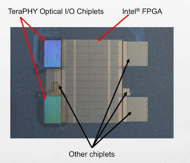
Stratix 10 system-in-package
The Intel phased-array radar system-in-package is designed to takes in huge amounts of RF data that is down-converted and digitised using an RF chiplet. The data is then pre-processed on the FPGA and sent optically using Ayar Labs’ TeraPHY chiplets for further processing in the cloud.
“To digitise all that information you need multiple TeraPHY chiplets per FPGA to pull the information back into the cloud,” says Saleh. A single phased-array radar can use as many as 50,000 FPGAs.
Such a radar design can be applied to civilian and to military applications where it can track 10,000s of objects.
Moreover, it is not just FPGAs that the TeraPHY chiplet can be interfaced to.
Large aerospace companies developing flight control systems also develop their own ASICs. “Almost every single aerospace company we have talked to as part of our collaboration with Intel has said they have custom ASICs,” says Saleh. “They want to know how they can procure, package and test the chiplets and bring them to market.”
It is one thing to integrate a chiplet but photonics is tricky
TeraPHY chiplet
Two Intel-developed technologies are used to interface the TeraPHY chiplet to the Stratix 10 FPGA.
The first is Intel’s Advanced Interface Bus (AIB), a parallel electrical interface technology. The second is the Embedded Multi-die Interconnect Bridge (EMIB) which supports the dense I/O needed to interface the main chip, in this case, the FPGA to a chiplet.
EMIB is a sliver of silicon designed to support I/O. The EMIBs are embedded in an organic substrate on which the dies sit; one is for each chiplet-FPGA interface. The EMIB supports various bump pitches to enable dense I/O connections.
Ayar Labs’ first TeraPHY product uses 24 AIB cells for its electrical interface. Each cell supports 20 channels, each operating at 2Gbps. The result is that each cell supports 40Gbps and the overall electrical bandwidth of the chiplet is 960 gigabits.
The TeraPHY’s optical interface uses 10 transmitter-receiver pairs, each pair supporting 8 optical channels that can operate at 16Gbps, 25Gbps or 32Gbps. The result is that the TeraPHY support a total optical bandwidth ranging from 1.28Tbps to 2.56Tbps.
The optical bandwidth is deliberately higher than the electrical bandwidth, says Saleh: “Just because you have ten [transmit/ receive] macros on the die doesn’t mean you have to use all ten.”
Also, the chiplet supports a crossbar switch that allows one-to-many connections such that an electrical channel can be sent out on more than one optical interface and vice versa.
For the Intel FPGA system-in-package, two TeraPHY chiplets are used, each supporting 16Gbps channels such that the chiplet’s total optical I/O is up to 5.12 terabits.
Ramifications
Saleh stresses the achievement in integrating optics in-package: “It is one thing to integrate a chiplet but photonics is tricky.”
Ayar Labs flip-chips its silicon and etches on the backside. “Besides all the hard work that goes into figuring how to do that, and keeping it hermetically sealed, you still have to escape light,” he says. “Escaping light out of the package that is intended to be high volume requires significant engineering work.” This required working very closely with Intel’s packaging department.
Now the challenge is to take the demonstrator chip to volume manufacturing.
Saleh also points to a more fundamental change that will need to take place with the advent of chip designs using optical I/O.
Over many years compute power in the form of advanced microprocessors that incorporate ever more CPU cores has doubled every two years or so. In contrast, I/O has advanced at a much slower pace – 5 or 10 per cent annually.
This has resulted in application software for high-performance computing being written to take this BW-compute disparity into account, reducing the number of memory accesses and minimising I/O transactions.
“Software now has to be architected to take advantage of all this new performance and all this new bandwidth,” he says. “We are going to see tremendous gains in performance because of it.”
Ayar Labs says it is on schedule to deliver its first TeraPHY chiplet product in volume to lead customers by the second half of 2020.

ADVA runs the rule over its TeraFlex platform
Gazettabyte talks to Jörg-Peter Elbers about the recent trial of ADVA’s FSP 3000 TeraFlex platform in Tele2’s network and gets his views on industry trends.

It is early morning and the air is cool. I'm seated outside at a coffee bar in Herzliya’s marina awaiting Jörg-Peter Elbers, senior vice president, advanced technology, who is in Israel visiting local ADVA staff.
He arrives as the bar opens and we are the only customers.
Just as we are about to start, the waitress informs us that the barista has yet to arrived. Breakfast can be ordered but we must wait for coffee.
Flexing the TeraFlex
ADVA trialled its TeraFlex platform on a Tele2 route between Tallinn and Frankfurt.
First detailed in 2017, the TeraFlex is a one-rack-unit (1RU) stackable chassis that supports three hot-pluggable 1.2-terabit modules or ‘sleds’. Each sled uses an Acacia AC1200 coherent module that supports two line-side wavelengths, each capable of coherent transmission at up to 600 gigabits-per-second (Gbps).
The TeraFlex was designed to address the needs of large-scale data centre operators that want power-efficient, high-capacity and compact platforms. But interest in the platform has broadened to include telcos and research and educational network operators.
For the trial, the transmission distance was increased by using loopbacks at the route’s locations. From an operational perspective, it means equipment is needed at one site only. The network also features reconfigurable optical add-drop multiplexers (ROADMs) at all the intermediate sites.
Data was sent in 100-gigabit increments over a spectral slice. A spectral slice is a relatively new concept whereby an operator leases a portion of the unused spectrum on a fibre to interested third parties.
The optical performance achieved includes sending a 500-gigabit optical signal over 1,016km and a 200-gigabit signal over 5,738km.
The TeraFlex has also been trialled by Telecom Italia in its backbone network. A 600Gbps wavelength was sent over a distance of 100km on an optical route designed for 10Gbps while a 300Gbps signal was sent over a distance of 2,500km.
ADVA used network telemetry data gathered by the TeraFlex to boost overall optical performance. “That was also an intention of the trial: how hard can we drive the system and what is the top-line performance we can get,” says Elbers.
The TeraFlex has also been trialled by Telecom Italia in its backbone network. A 600Gbps wavelength was sent over a distance of 100km on an optical route designed for 10Gbps while a 300Gbps signal was sent over a distance of 2,500km.
Differentiation
ADVA dismisses the notion that TeraFlex’s optical performance is dictated solely by Acacia’s AC1200 module such that the scope for platform differentiation is limited when compared with competitors’ designs that also use the Acacia module.
“The TeraFlex does use certain hardware but there is a tremendous amount of configuration flexibility, literally thousands of configurations you can use,” says Elbers.
These include different modulation formats and whether fractional quadrature amplitude modulation (QAM) is used. Fractional QAM is a feature of Acacia’s coherent module whereby two adjacent modulation formats, for example, 8-QAM and 16-QAM, are each used for a percentage of the transmission time to fine-tune the data rate. The baud rate for a given data rate can also be altered to adapt the spectrum used for the transmission.
For the trial, a QPSK reference signal was first sent, a signal that will go the furthest. Based on the performance achieved, a decision is made as to whether the data rate transmission performance can be bumped up, says Elbers.
Networks are run conservatively, he says. At the start of a link’s life, the large safety margin built-in can be exploited to cram more data across a link.
“I might run into issues at the end of the life of the system but I can drive the system harder at the beginning,” says Elbers. “The result is more capacity from the start and better economics.”
Elbers says that optimising the network, even at its end-of-life stage, by exploiting the capacity available in each slot and optimising the spacing and data rate, a 30 percent capacity improvement can be achieved compared to a non-optimised network.
But the bigger potential is if the operator is willing to operate the line system using lower margins, adjusting as required over its operational life, whereby a doubling of capacity is possible.
Jörg-Peter Elbers
600G versus 800G
Elbers says that there is a market perception of a 600 gigabit-class of coherent performance and an 800 gigabit-class. Systems vendors Ciena and Infinera have announced solutions that deliver 800 gigabits per wavelength.
But such solutions do not yet exist, he says, adding that operating at a lower symbol rate per wavelength results in a lower implementation penalty. “Components are imperfect compared to the theoretical performance and the closer you stay with the maturity curve of the technology, the lower the delta is,” says Elbers. “With 60 gigabaud [GBd] and QPSK modulation, you are very close – sub 1 decibel - from the theoretical performance; that is what we can get.”
ADVA also points out that a TeraFlex sled can deliver 1.2 terabits using two optical wavelengths and a single coherent DSP.
For the Tele2 trial, the TeraFlex also delivered 800 gigabits of data using a 125GHz-wide channel. “This was a superchannel configuration,” says Elbers.
The AC1200 can operate close to 70GBd while Infinera’s ICE6 will operate at 88GBd using sub-carriers while Ciena’s WaveLogic 5 can operate at up to 95GBd.
“There are certain technology evolution steps; 95GBd appears a half step,” he says. The industry has gone from thirty-something to sixty-something gigabaud and now the aim is to double it again. Elbers believes 120GBd and even 140GBd will be possible.
“It is not just the building blocks but integration which will form more and more a key part,” says Elbers. “Bringing everything as close together as possible.” This is needed to tackle the ever-increasing challenge of radio frequency (RF) design as the symbol rate continues to rise.
Acacia’s acquisition
When Cisco announced in July its intention to acquire Acacia, ADVA commented that such developments are to be expected as networks become more open and disaggregated.
ADVA also pointed out that Cisco intends to run Acacia as a component business unit and will continue to sell to all equipment makers while Ciena’s Optical Microsystems unit is making its WaveLogic coherent DSPs and module technologies available to the wider market. And with companies such as NEL and Inphi, merchant DSP experts will continue supplying the market.
While not going into detail, Elbers points out that it is common practice to have clauses in contracts that ensure continuity of supply under such circumstances. He also adds that designing in another coherent DSP into a platform such as the TeraFlex is “a big decision” but that the TeraFlex has been architected with such modularity in mind.
Vertical integration
ADVA has a team that addresses the company’s technology needs to help the company decide whether to make or buy. “What areas makes sense for us to do on our own and which areas does it make sense to just buy from a merchant vendor,” says Elbers.
The company has always designed its optical amplifier solutions and developed its MicroMux solution that allows low-rate client signal interfaces to interface efficiently to the high-capacity TeraFlex.
Only a few companies will continue to make their own coherent DSPs, he says, especially as next-generation designs move to the costly 5nm CMOS process.
Silicon photonics design expertise is another skill ADVA has. “Silicon photonics democratises component development and we have activities in that area involving coherent engines and optics and we see the potential there,” says Elbers.
Our interview ends and we make our way to a taxi rank beyond the marina so that Elbers can travel to Ra’anana where one of ADVA’s two local offices is located.
We find a driver before realising he is not first in the rank. The cab driver that is first in the rank strides towards us and a heated discussion between the drivers ensues. Agreement is reached and we move to the first cab but not before Elber’s new driver restarts the argument. Eventually, Elbers sets off for the rest of his day.
The morning air has heated up.
Co-packaged optics to debut with 25.6 terabit switch chips
The second article in a series on co-packaged optics.
Part 2: Broadcom - a switch-chip vendor

Source: Gazettabyte
The hyperscalers require ever more switching capacity in their data centres to scale the applications they run. A hierarchy of connected switches fitted with optical interfaces is used to provide the pathways that link the tens of thousands of servers found in data centres.
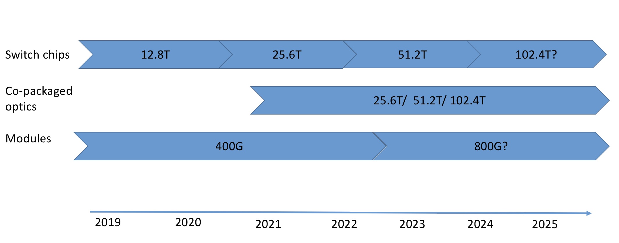
Silicon vendors are responding to this need by doubling the capacity of their switch chips every two years. The largest switch chips have a 12.8-terabit capacity and the first 25.6-terabit devices are expected next year. This relentless pace, however, is one that the optical module makers are struggling to match.
“It is a problem for the optics industry,” says Robert Stone, Distinguished Engineer at leading switch chip player, Broadcom. “The cadence at which we can evolve silicon generally moves a lot faster than the optics guys can monetise a generation of investment, and then reinvest it.”
Co-packaged optics
The result is a schism between the optics and the switch ICs, says Stone.
Data centre operators have had to use 100-gigabit interfaces across two generations of switching silicon. The lag between the two camps is also evident in how certain hyperscalers are adopting 200-gigabit pluggables as a stopgap measure before 400-gigabit modules become mainstream.
The doubling of chip capacity every two years will continue to challenge the optical module engineers. Can faster, power-hungry pluggable optical modules - 800-gigabit modules will follow 400-gigabit ones - fit on the faceplate of a switch at the density required? Currently, 32 400-gigabit optical modules fit on the front panel of a 1-rack-unit (1RU) switch. And if not, what are the alternatives to pluggable modules?
Two options are being pursued by the optical industry.
One is moving the optics from the switch’s front panel onto the motherboard. Such on-board optics shorten the length of the high-speed traces on the printed circuit board (PCB) linking the switch ASIC and the pluggable optics. In turn, the freed-up space on the front panel by ditching pluggables improves the ventilation and cooling of the switch.
The second option, co-packaged optics, places the optics with the ASIC in the same package.
Placing the optics next to the switch chip enables the high-speed serialiser-deserialiser (serdes), the circuit that gets data on and off the chip, to be simplified. No longer will the serdes have to drive very high-speed signals all the way to the front panel’s pluggables. This simplifies the PCB design, constrains the switch chip’s overall power consumption given how hundreds of serdes are used, and reduces the overall die area they consume.
>
“It may just be that operators hedge their bets by deploying half co-packaged optics and half conventional optics to make sure they don’t completely strand themselves”
At a recent panel session at the OFC show, held in San Diego in March, entitled Beyond 400G for Hyperscaler Data Centres, the consensus was that front-panel pluggable optics will continue for at least two more generations of switch chip: 25.6 terabits and 51.2 terabits.
“We can build such systems with conventional front-panel optics with a bit of hard work,” says Stone, a participant in the OFC panel discussion. For example, a 2RU-high 25.6-terabit switch platform will accommodate 64, 800-gigabit modules.
The ‘hard work’ refers to tackling the heat generated by the chip and, in particular, the power consumed all the serdes. But these are engineering challenges, not fundamental physics issues, they can be overcome, says Stone.
But there is an industry acceptance that continuing to increase the speed of client-side pluggables has a limited future and that change is coming.
Overlapping worlds
Stone’s belief is that co-packaged optics will first be deployed alongside pluggables, enabling the hyperscalars to deploy both technologies in their data centres. This will reduce the risk associated with introducing the new technology, such as a supply constraint or a reliability issue.
Indeed, this is the guidance Stone has been giving the silicon photonics players developing co-packaged optics. It is all well and good for a company to come up with very low power, dense wavelength grid optical interface design, he says, but the co-packaged device will need to interoperate with conventional front-panel pluggable optics.
“It may just be that operators hedge their bets by deploying half co-packaged optics and half conventional optics to make sure they don’t completely strand themselves,” says Stone.
Stone is confident that there will be co-packaged optics solutions with the advent of 25.6-terabit and 51.2-terabit switch chips.
“I don’t think they will be necessary,” he adds. “It will be more a cost and power optimisation in those generations.” But pursuing co-packaged optics provides a way for companies to differentiate themselves and innovate.
Stone also notes that certain switch chip vendors are separating the serdes input-output (I/O) circuitry, resulting in standalone dies that surround the packet-processing core. Such serdes ‘tiles’ lend themselves to a co-packaged design.
“Once you have split off the I/O, you may then switch the electrical I/O to optical I/O,” says Stone. “Obviously, there is a lot of detail to be worked out but the move away from a big monolithic-chip package makes it friendlier to do such integration.”
Challenges
But co-packaged optics presents its own challenges.
Stone says that it is still uncertain whether co-packaged optics will be a must for the switch chip generation after 51.2 terabits although he believes that is when such optics becomes compelling.
“Having said that, it is not a complete slam-dunk in that generation either because now you are aggregating a lot of heat in a very small space,” he says. “If you take a 100-terabit chip, or whatever the number will be, and you pack all that optics onto it, trying to cool that is going to be very hard.” That suggests water-cooling will be needed as air-cooling will not be sufficient.
Unless there is a need to solve a feasibility challenge, designers will continue to cling to what they have done historically. “It is comfortable, people know how to do it, and the supply chain is already built up,” he says. All these factors change with the embrace of co-packaged optics.
The industry has yet to run into that feasibility gap but what has changed is that the industry now acknowledges that it is coming.
Richard Wilson

Richard Wilson
An important part of my career as a journalist was spent at the UK newspaper, Electronics Weekly.
The editor at the time was Richard Wilson. For several years I sat opposite him; despite having an office, Richard worked with us all. It was an exciting time to be covering the chip industry and we all worked hard. Richard was a wonderful boss and a great conversationalist.
>
“A talented journalist and loved the complexities of the electronics industry but he had many interests and talents that were not given expression in that environment.”
I remember his joy the day after the Labour Party won the UK election in 1997 and he described how he had not slept watching the results come in (and the following day was a news day!)
He was a lovely, gentle man. I often wondered what he was doing at Electronics Weekly. He was a talented journalist and loved the complexities of the electronics industry but he had many interests and talents that were not given expression in that environment.
Electronics Weekly wasn’t always an easy workplace but I look back at those years and think it was the most vibrant place I’ve worked at. The place was filled with characters and Richard added to the pleasure of being there.
I think of Richard with huge fondness and am grateful to have known him. I last saw him in 2003 but despite the elapsed time, I feel his loss deeply.

A voyage around work
The first in a series looking at the experience of work in 2019.

Source: Mark Seery
To land your ideal job, the suggestion is first to find your passion. Indeed, one college in the US promises to guide its students to find their life purpose by teaching them three things: what they are good at, what they are passionate about, and what the world needs.
Assuming you are lucky enough to align all three elements, challenges are still likely. How do you maintain a work-life balance? And what happens over time when, despite having fulfilling, challenging work, part of your creative self remains untapped?
This has been the experience of Mark Seery (pictured below), who was a senior staff member at Juniper Networks, responsible for helping shape the networking company’s strategy.
Impetus for change
Seery first felt a murmuring for change in 2015 but only in 2018 did he act.
In 2015, he returned to Australia to spend time with his dying mother. Work commitments were such that his stay was limited. Seery’s mother died a week after he returned to the US and he travelled again to attend the funeral.
Last July he also visited Australia, this time to spend eight days with his brother who was celebrating a birthday. Again, because of work commitments, he felt he couldn’t spend too much time visiting yet the landmark birthday was something he felt he could not miss.
“The idea that work pressure would mentally impinge on even an eight-day stay made me realise my life was not well-balanced,” says Seery.
Just after the trip he informed his manager that he was resigning in order to take a sabbatical. A key motivation for the break was his desire to travel.
Seery chose to make a clean break rather than negotiate time off: “I didn't want to feel that there were any limitations as to what I could do on my sabbatical; I wanted to be free and see where that takes me.”

Source: Mark Seery
A leaving date was set for mid-October, his tenth anniversary at Juniper. “Ten years at Juniper seemed a significant milestone to me,” says Seery.
Since then, Seery has completed the first leg of his travel, visiting eight countries in Asia. And this month he is embarking on a second trip, visiting the Antarctic and Patagonia.
He has also set up his own business, to advise companies on finding their focus.
Career
As a child, Seery’s education was disrupted due to ill health. His first job, at 17, was in banking while at night he studied computer science. Seery credits his mother for encouraging him to pursue computing, a passion since childhood.
Seery’s first opportunity to move from traditional banking to IT involved joining the bank’s network operations. This included automatic teller machines, branch networks and data centre interconnect. “The network operations area, which reminded me of the Star Trek flight deck, drew me to choose network operations,” he says.
He progressed to network operations support, network design and systems programming.
His next step was to leave Australia for the US where he joined several Silicon Valley start-ups, pursuing such technologies as next-generation access, multi-protocol/ virtual routing and all-optical networking.
In 2002, Seery became an analyst, joining market research firm, RHK, that was subsequently acquired by Ovum. And it was while at RHK covering the switching and routing market that he was noticed by Juniper and enticed to join. Juniper’s routing group hired him as they felt he could help on some strategic issues.
From there, he expanded his strategic skills, joining the corporate strategy team where he undertook several roles. These included market intelligence, running CEO staff-level competitive war rooms and creating materials for quarterly company board meetings.
Seery’s role was to help give the company the data it needed to determine how best to meet its goals for the coming year. A company must determine what actions will have the most impact in meeting the targets and must budget in a way to give the best chance of meeting those goals.
“The real struggle in any strategy is how to get it executed,” says Seery. “And an important part of getting it executed is the right allocation of resources.”

Source: Mark Seery
Seery describes how different units in a company - the sales groups, product groups and the CFO office - all have their own views and agendas. The role of the strategy group is to be independent and provide analysis to help the decision makers plot the company’s course.
Corporate war-room work involved more tactical, shorter-term strategy, such as how to improve the performance of a specific business or a product.
Eventful years
Seery’s first years at Juniper were eventful ones. He joined soon after a new CEO who brought with him several senior staff, all from outside the industry. This required a lot of work preparing data and documents so that the company’s senior staff were all on the same page.
>
“We all use the term value chain and we all have an idea about what it means. But it is only when you get your hands dirty trying to change the value chain that you really understand what it means.”
In 2009, the market hit a recession after the global financial crisis of 2008. And in 2011, it became clear that the European market was getting worse. Such economic disruptors required a lot of replanning.
It also became clear that the capital expenditure budgets of many of the service providers would no longer be growing and that the biggest part of their spending would go on the radio part of their networks. “The thing you did best is not going to grow anymore. What does that mean for the company?” says Seery.

Source: Mark Seery
And then there were new developments that occupied Seery as part of his business model strategy role.
One was the observation that software was becoming increasingly important, coupled with the huge disruption that is the cloud. Such developments had to be translated in terms of their significance for Juniper.
He also had to grapple with the idea - one affecting companies across many industries - that recurring revenue such as from subscriptions may benefit a company’s evaluation on Wall Street more than that of a company selling products only. Issues to be addressed here include how such a change would affect the company’s revenues, the operational changes required, the products Juniper should develop for such a model, and how to enable the sales force to sell such products.
“We all use the term value chain and we all have an idea about what it means,” says Seery. “But it is only when you get your hands dirty trying to change the value chain that you really understand what it means.”
The business model work was a big change for Seery, shifting him from a highly analytical role to one that involved engaging with many functions of the company.
His growing disquiet at Juniper wasn’t due to the stress of needing to continually produce deliverables, nor the demanding nature of his work. “It was more a feeling that I was missing out on something else,” he says.
Parting
Seery provides a multifaceted answer as to why he decided to resign.
First, his work on business modelling had been largely defined and was moving to the operational phase. It meant his day-to-day involvement was no longer required. This led him to question what he wanted to do next.
He also felt that, for a long time, part of him remained unfulfilled. “In a corporate context, there are certain expectations, the scope of things you talk about, the scope of things you express,” he says. “People in a corporate environment don't really care about some of the bigger issues you have as a human being.”
Companies focus on meeting targets each quarter and your life can become all-consuming to fulfil that ongoing short-term goal. The result, he says, is that a part of you gets pushed aside.

Source: Mark Seery
“You make a lot of sacrifices on things you are passionate about; things you enjoy,” says Seery. “If what you are passionate about is driving a business, then great, but not all of us are made that simply.”
Seery has spoken to people who have been more successful at managing their work-life balance. “Could I have have found a better balance in my ten years at Juniper? Maybe, but the fact is I didn't.”
It is these issues that led Seery to identify what was important to him and to focus on that.
Seery admits the decision to leave a secure and well-paid position at Juniper was extremely hard. But he says that he has a great appreciation and gratitude for the affluence he has already achieved, reinforced by his travel experiences.
One of the today's great challenges is ever-increasing consumption. The key is to step back and be grateful for what you already have, he says: “There is nothing wrong with striving for more, but craving for it and comparing yourself to others can be a trap.”
Travel
Travel is something Seery did repeatedly when he was younger but it inevitably dwindled with work and family commitments.
>
“One young man in Myanmar told him that his fishing village didn’t have electricity till 2008 and didn’t have the internet till 2010”
For him, travel is a way to understand the human experience through other people’s stories. “I find when I travel, it has a real impact on me,” he says.
Seery worked with a travel company to plan his itinerary for the South East Asia trip, including having local guides in each town he visited.
“I had a structured itinerary with dates and places, though I had the ability to change what I wanted to do on any given day,” says Seery. “Having some structure and predictability is helpful when you have a family at home worrying about you.”

Source: Mark Seery
South East Asia
Seery had travelled via work to developed parts of Asia including China, Japan and South Korea. But travelling through less developed parts of Asia is a very different experience, he says.
He spoke to one young man while visiting Myanmar who told him that his fishing village didn't have electricity till 2008 and didn't have the internet till 2010.
Villagers continue to cook with fire rather than using an electric stove, claiming they don’t know how to use one, however, it could be that they can’t afford one, he says. They also use hay for one cooking effect and wood for another.
“The young man told me that the village had had no visibility into protests taking place in cities across the country until the advent of the internet. “They use Facebook, not Google, as a search engine, to see videos and get information about what is going on,” says Seery. “In the modern context, with everything that is going on with Facebook, we probably think that is somewhat scary.”
But the young man added he’d rather get on Facebook and talk to someone who lives in a city and ask them what is going on than trust what the Government tells him. “An interesting insight into why they view Facebook as a credible source of information,” says Seery.
Other examples of the impact of the internet include the way football is viewed. Before mobile data, villagers had to pay one villager that owned a huge satellite dish to watch an English Premier League match. Now they all watch on their phones.
Seery also highlights the ongoing tension between traditional life and modernity. He tells how when visiting rural villages in Laos one is struck by the poverty and lack of modern conveniences. It is easy to judge and wonder how they enjoy living there, he says, but they do.
However, the long-standing tradition of the elders sharing the history of the tribe and life stories around a campfire is changing. “Now, you get around the campfire and some kid with a cellphone is telling everybody what is going on in the rest of the world,” says Seery. “They are all very happy with how they are living until they find out how other people are living.”
Seery originally planned to be in Asia for a month but after talking with his wife and son who were about to oversee some home renovations, they all concluded that he should extend his trip. So he joined a tour group as part of the India and Nepal leg of his journey that extended the trip by several weeks.
What next?
The imminent trip to Antarctica will last 12 days with five days required to travel between Antarctica and Latin America. Once at the Antarctic, two nights will be spent camping on the ice, and there will be snowshoe walking. There are also Zodiac boats and options for kayaking and mountaineering.
In Patagonia, the trip will involve a three-day hike, an overnight horse-riding and camping trip, and several shorter hiking trips.
Seery’s new venture is a consultancy and research company called Bohcay. “It is a play on the photography term, Bokeh, the soft blurring you get behind a portrait,” says Seery.
The company’s aim is to help clients retain a systematic focus on what is important in terms of what they are doing, he says. Seery is in the process of closing his first customer for a short engagement.
“It is all part of exploring what I want to do after I finish my travel,” says Seery.
People that have met Seery since his return from his Asia trip comment on how he has lost weight and looks more relaxed. He is also exercising regularly, something that was only episodic during his time working.
He himself feels a weight has been lifted by no longer being burdened by the thought of sacrificing what he really wants to do.
“The more I travel, the more I will feel I have addressed that thing that was going on with me,” he says.
Further information
Bohcay website, click here
Mark Seery’s travel blog, click here
Kim Roberts: The 2019 John Tyndall Award winner
Roberts has been awarded the 2019 John Tyndall Award by The Optical Society (OSA) and the IEEE Photonics Society in recognition of his “pioneering contributions to the development of practical coherent communication systems”.
“It is well deserved,” says Seb Savory, who first knew Roberts when they both worked at Nortel and who is now an academic at the University of Cambridge working on joint projects with Ciena. Ciena acquired Nortel in 2010.

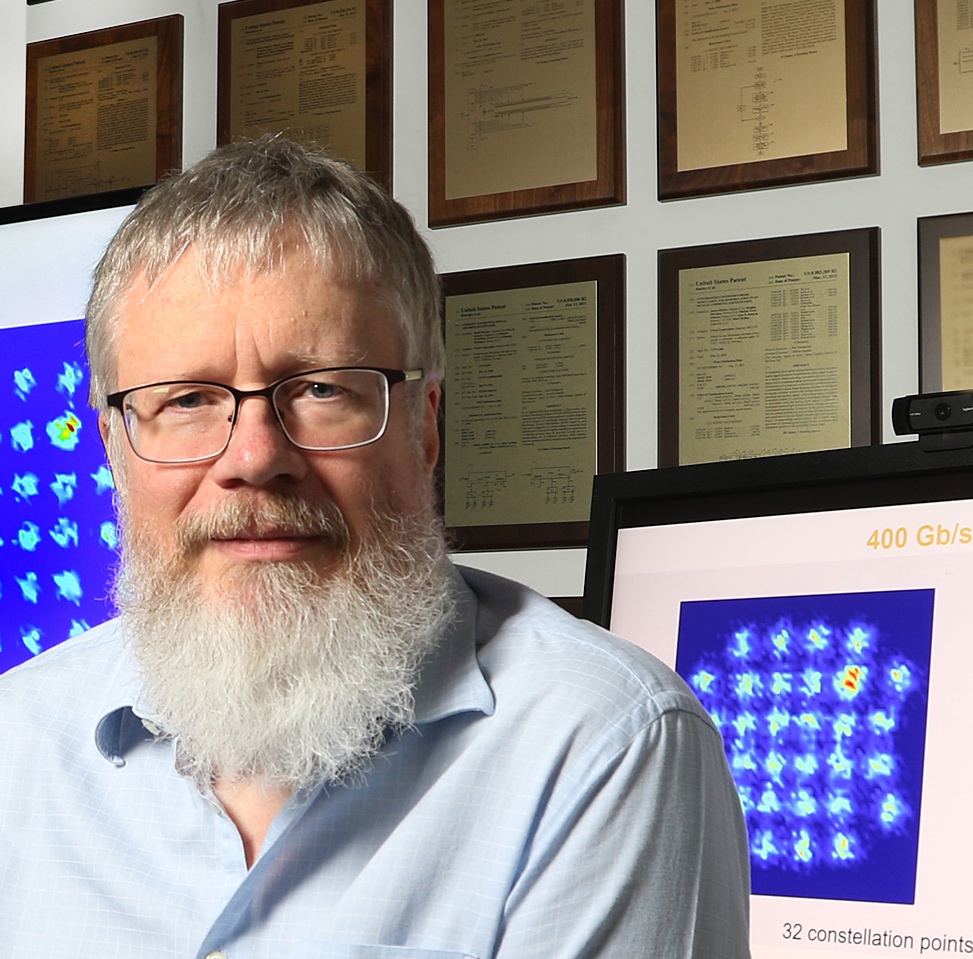
Kim Roberts of Ciena. On the wall are some of his 160 patents while on the screen is an image of a 32-point constellation produced by the WaveLogic Ai coherent modem. Source: Ciena.
“The best measure of Kim’s contributions and impact is the simple fact that the practical coherent optical communication systems that Kim pioneered are now the gold standard for high-capacity fiber-optic systems,” says Steve Alexander, Ciena’s CTO. “They have become the foundation of the fabric for how the world connects, having been deployed by nearly every large network operator on the planet.”
“Roberts was among the very first who introduced electronic signal processing in optical communications," says Professor Ioannis Tomkos at the Athens Information Technology Center (AIT). Initially, the signal processing was at the transmitter - electronic-based equalisation for pre-compensation in direct-detection systems - and then at the receiver. “Roberts’s ideas have made coherent detection practical and revolutionised the industry,” says Tomkos.
Meanwhile, his boss, Dino DiPerna, vice president, packet optical platforms R&D at Ciena, describes Roberts as having one of the most brilliant minds he has encountered.
Education
Roberts read electronic engineering with an emphasis on maths at the University of British Columbia in Vancouver, Canada. “I took courses and took extra courses to get all the requirements of an Honours maths degree,” says Roberts.
Why add maths to an already demanding degree? A recognition of the importance of having a firm grounding in maths for electronic engineering or simply a love of the subject? “It is fun,” says Roberts.
His exploration of maths is ongoing. Most Fridays, Roberts works from home where, after catching up with email, he studies maths. “It is not related directly to engineering, I just learn a new branch of mathematics,” says Roberts. The goal is to learn something new that may or may not help trigger ideas in the future. Overall, the practice has proved very fruitful, he says.
After his undergraduate studies, Roberts gained a fellowship to pursue a Masters degree in a neurological lab developing diagnostics tests for the disease, Multiple Sclerosis.
“Signals were measured on the brain and my task was to identify whether this was normal or abnormal, indicating Multiple Sclerosis,” he says. “I baked cinnamon buns to bribe my friends to come in and be the normals; I needed 25 normals.” His resulting system outperformed a neurologist looking at the same data.
Roberts finished his Masters in the winter of 1983-84. It was a period of recession and he had two job offers: one was to continue at the lab and the second was at Nortel.
“I went off to Nortel and learnt about optics,” says Roberts.
Career
Roberts has overseen several notable projects in his career, as highlighted in the press release announcing the 2019 John Tyndall Award.
These include Nortel’s Superdecoder, terrestrial optical amplifiers for 2.5- and 10-gigabit transmissions, bringing 10-gigabit optical transport to market including developing the first WaveLogic IC, and coherent-based optical transmission.
The Superdecoder was Nortel’s internal name for the application of signal processing to intensity-modulated signals received using a direct detection-based optical receiver.
There are three critical parameters involved with intensity-modulated direct detection (IMDD), says Roberts: the gain of the avalanche photo-detector, the phase of the clock making the decision, and the ‘slicing level’ - the sampling threshold - which may not necessarily be at 50 percent.
The detection circuitry includes the slicer and a flip-flop. The slicer determines if the received bit is a 1 or 0 that is then latched into the flip-flop at the appropriate time. “If it made an error, it made an error,” says Roberts. “In a 2.5-gigabit system there was no error correction, so that was a customer error.”
Nortel’s cleverness was to add two more slicers and flip-flops in parallel to the central channel decoding the actual data. These extra detector channels could have different sampling levels that were executed at different times. The Exclusive-OR logical operator was applied to each output of the extra channels with the central channel. If they differed, a ‘pseudo-error’ was called.
While pseudo, such errors add value in that they help identify where the centre of the eye diagram is to optimise the actual data detection.
“You want it [the detection] at the optimum time and voltage,” says Roberts. “You try to reduce the number of errors to get the optimum positioning of the data channel by doing high-speed measurements in parallel.”
The project came about after a former boss took an internal course on gallium arsenide (GaAs) circuits and chose this as his course project.
“The two of us designed the GaAs circuit and I then went on to do the mathematics of how do we use this idea,” says Roberts. “It went from a course project into what we do in all our IMDD receivers.”
Optical amplifiers and 10 gigabit
Roberts led the Nortel team that developed terrestrial optical amplifiers. “Optical amplifiers had been used for transatlantic links and we developed optical amplifiers to go 2.5 gigabit and 10 gigabit,” says Roberts.
The challenges included the physics, which was new, and determining how to make optical amplification into a product that customers could engineer, install and manage.
Roberts also managed the team that did the science and the prototypes that eventually became Nortel's 10-gigabit product that started shipping in 1995.
“He was one of the big forces behind getting to 10 gigabit [optical transport],” says Savory. “Nortel was the one that went to 10 gigabit when others were saying you couldn’t do 10 gigabit.”
Pre-compensation & the WaveLogic chip
In the early 2000s, Roberts started working on what became Nortel’s first WaveLogic IC. Here, electronics was used as an aid to counteract optical transmission impairments.
"He developed digital signal processing schemes for pre-distorting the signals at the transmitter, with the goal to compensate for transceiver imperfections and chromatic dispersion-induced distortions as the optical signal pulses are propagating over the transmission fibre,” says Tomkos. “Signal pre-distortion and chromatic dispersion effects on the propagating optical pulses counteract each other as they travel along the fibre so that an almost clean signal is detected at the receiver.”
“There was a realisation by our team that if we modulate the complex electrical field - not just turn the light on and off - then we could compensate anything we wanted to before we transmitted,” says Roberts. “We could do digital linear filtering for the chromatic dispersion that was going to be on the line.”
Using an IC at the transmitter meant the receiver circuitry didn’t need to change. It also meant that electronics could replace the spools of chromatic dispersion-compensation fibre that was, at the time, the solution used. Such fibre spools were costly and added optical loss.
According to Tomkos, Nortel only went public about its pre-distortion technique once similar ideas were published in a paper by an academic.
“I started going around the world preaching a new gospel that dispersion is your friend, dispersion is good,” says Roberts. “That we can fix enormous amounts of dispersion and that the dispersion helps to smear out nonlinearities.”
However, the claim was met with skepticism. The issue, says Tomkos, was the nature of the distorted transmitted pulses: they had a very high peak-to-average power ratio. “When you send very high power signals, it generates non-linear effects,” says Tomkos. Nortel’s competitors claimed the technique wouldn't work and it had no future.
“It took a few years of preaching for the community to become believers,” says Roberts.
Developing the pre-distortion chip - what became the first WaveLogic device - subsequently led to Nortel’s development of the coherent optical receiver.
>
“I like to build things and electronic engineering gives you the tools to be able to take your ideas and build them”
Coherent receiver
The critical circuit within the WaveLogic IC was its high-speed digital-to-analogue converter (DAC) implemented in CMOS. The overall bit rate was 10.7 gigabits-per-second (Gbps) such that the DAC operated at twice the rate - over 21 gigasamples-per-second - to satisfy the Nyquist sampling theory.
“Once we realised we could build these, we realised we could build the analogue-to-digital converter that could run just as fast and we could build [a] digital coherent [system],” says Roberts. Until then, most of the work had looked at analogue optical coherent which Roberts describes as very hard.
“Four of us in a room sketched through on a whiteboard the pieces we needed and we concluded we could build it,” says Roberts.
“It was the same bet-your-houses philosophy with the move to coherent [that was used by Nortel for 10 gigabit],” says Savory. “Kim was very much leading the team that put together the coherent receiver.”
People thought coherent was a nice idea but that it would never happen, says Savory, the issue being the effort required to develop the coherent digital signal processor (DSP).
The coherent receiver - the optics and the coherent DSP - not only solved the problem of chromatic dispersion but also overcame the issue of polarisation mode dispersion which, at the time, was a barrier to achieving faster optical transmission speeds of 40Gbps and higher.
By handling the enormous amounts of polarisation mode dispersion, the coherent receiver could work anywhere a 10-gigabit wavelength would work, says Roberts: “You just plugged us in; it made it very easy for customers to deploy.” And that led to coherent’s commercial success.
Savory mentions how Nortel’s coherent receiver work was submitted as a post-deadline paper at an ECOC conference and was rejected. “I remember chatting to Kim afterwards who, like me, was despondent given the technological breakthrough this represented,” says Savory.
He encouraged Roberts to submit the work to the OSA’s Optical Express journal, where it was subsequently published in 2008 with Roberts as the senior author. “It is now seen as one of the key papers,” says Savory.
Since then, a total of four generations of WaveLogic devices have been announced, the latest being Ciena’s WaveLogic Ai. Indeed, Roberts’ job title is Vice President of WaveLogic Science.
It was my last meeting on the final day of the OFC 2010 show. I was being showcased Nortel’s first 100-gigabit coherent system in a private room reserved for prospective customers. It was also the week that Ciena closed the acquisition of Nortel.
I was talked through the various components of the system. The spectrum analyser display was also explained - the system used two tones per channel, each carrying 50-gigabits of data - while on a whiteboard, constellation points and modulation schemes were drawn to explain the theory.
Despite being exhausted after a long week and poor sleep due to the time zone difference, I left the room feeling energised and elated. I had witnessed the most impressive technological display just as the show was winding down. The 100-gigabit coherent platform had also been explained to me by a patient and clearly authoritative Nortel engineer.
That was my first encounter with Kim Roberts. (Editor, Gazettabyte.)
Talents
Savory describes Roberts as a conceptualiser: “You get some people that can do the maths but don’t have the conceptual understanding.” Roberts can do both. “He is also a prolific inventor,” adds Savory: Roberts has 160 patents.
Roger Carroll, Ciena’s vice president, optical modem development, explains how Roberts can span from the theory down to the gate level of chip design. “That type of person is extremely rare,” says Carroll.
Ciena's DiPerna highlights another talent of Roberts: he is an unconventional thinker. “When you are creating, it is easy to get wrapped up in, 'Well, we can’t do that because of so and so',” says DiPerna. “Many brilliant, experienced people can fall into that trap and miss a chance to change the game.”
An example both DiPerna and Carroll cite was the development of WaveLogic 3 where Ciena first included soft-decision forward error correction (SD-FEC) and signal processing at the transmitter.
“The mathematics [of SD-FEC] had been around for a while but its implementation in a chip, at that time, that was magic,” says Carroll. “It had to fit in something that was manufacturable and with a reasonable power [consumption].”
At the time, other companies were getting 100-gigabit coherent to market using conventional hard-decision FEC while the WaveLogic 3 incorporate SD-FEC and signal processing at the transmitter.
“There was a lot of pressure at the time,” explains Carroll. “We stuck to our guns, Kim stuck to his guns and the chip helped pull us ahead in the coherent game.”

Kim Roberts and an example of his furniture making. "Squeezing more traffic through the cable: Maple, Cherry and stainless steel," he says. Source: Kim Roberts.
Work practices and leadership skills
The way Roberts works is something he has practiced throughout the development of the WaveLogic ICs.
A colleague will come into his office and the two will spend an hour or two arguing in front of the whiteboard. “Then, they [the colleague] will take a cell phone picture of the two big whiteboards and will go away and write out the maths proofs, or do a MATLAB simulation, or both,” says Roberts. “Meanwhile, someone else has come in with a different problem and we will go off in another direction and work through that.”
DiPerna says over the years he has been told how important Roberts is and asked what he was doing to keep Roberts excited.
First, he points out the working relationship he, Carroll and Roberts share, having all worked together for over 30 years. Second, DiPerna has made sure that Roberts is surrounded with top talent in the various teams he interacts with, such as Ciena’s analogue, opto, digital and ASIC teams.
“That is what turns Kim’s crank because he sees his ideas can come to life through that iterative process with the teams,” says DiPerna.
Career choice
If Roberts were to start university today, would he still choose electronic engineering?
“I would,” he says. “There are other opportunities but I like to build things and electronic engineering gives you the tools to be able to take your ideas and build them.”
Roberts says his son has also chosen this path, having just completed a PhD in electronic engineering dealing with the optimisation of optical networks in the face of optical non-linearities. “Not much imagination there to move very far away,” quips Roberts.
Roberts’ practical nature extends to making furniture (see image). His creations have appeared as part of his presentations, props that he uses to explain the physics, says DiPerna: “It is all part of the gawky character we love so dearly.
“The guy is a brother to us,” concludes DiPerna. “We are absolutely thrilled for him with this award; it is incredibly deserving.”

Access drives a need for 10G compact aggregation boxes
Infinera has unveiled a platform to aggregate multiple 10-gigabit traffic streams originating in the access network.
The 1.6-terabit HDEA 1600G platform is designed to aggregate 80, 10-gigabit wavelengths. The use of ten-gigabit wavelengths in access continues to grow with the advent of 5G mobile backhaul and developments in cable and passive optical networking (PON).
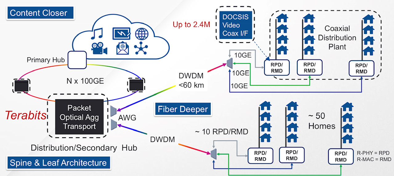
A distributed access architecture being embraced by cable operators. Shown are the remote PHY devices (RPD) or remote MAC-PHY devices (RMD), functionality moved out of the secondary hub and closer to the end user. Also shown is how DWDM technology is moved closer to the edge of the network. Source: Infinera.
A distributed access architecture being embraced by cable operators. Shown are the remote PHY devices (RPD) or remote MAC-PHY devices (RMD), functionality moved out of the secondary hub and closer to the end user. Also shown is how DWDM technology is moved closer to the edge of the network. Source: Infinera.
Infinera has adopted a novel mechanical design for its 1 rack unit (1RU) HDEA 1600G that uses the sides of the platform to fit 80 SFP+ optical modules.
The platform also features a 1.6-terabit Ethernet switch chip that aggregates the traffic from the 10-gigabit streams to fill 100-gigabit wavelengths that are passed to other switching or transport platforms for transmission into the network.
Distributed access architecture
Jon Baldry, metro marketing director at Infinera, cites the adoption of a distributed access architecture (DAA) by cable operators as an example of 10-gigabit links that are set to proliferate in the access network.
DAA is being adopted by cable operators to compete with the telecom operators’ rollout of fibre-to-the-home (FTTH) broadband access technology.
A recent report by market research firm, Ovum, addressing DAA in the North American market, discusses how the architectural approach will free up space in cable headends, reduce the operators’ operational costs, and allow the delivery of greater bandwidth to subscribers.
Implementing DAA involves bringing fibre as well as cable network functionality closer to the user. Such functionality includes remote PHY devices and remote MAC-PHY devices. It is these devices that will use a 10-gigabit interface, says Baldry: “The traffic they will be running at first will be two or three gigabits over that 10-gigabit link.”
Julie Kunstler, principal analyst at Ovum’s Network Infrastructure and Software group, says the choice whether to deploy a remote PHY or a remote MAC-PHY architecture is a issue of an operator's ‘religion’. What is important, she says, is that both options exploit the existing hybrid fibre coax (HFC) architecture to boost the speed tiers delivered to users.

The current, pre-DAA, cable network architecture. Source: Infinera.
In the current pre-DAA architecture, the cable network comprises cable headends and secondary distribution hubs (see diagram above). It is at the secondary hub that the dense wavelength-division multiplexing (DWDM) network terminates. From there, RF over fibre is carried over the hybrid fibre-coax (HFC) plant. The HFC plant also requires amplifier chains to overcome cable attenuation and the losses resulting from the cable splits that deliver the RF signals to the homes.
Typically, an HFC node in the cable network serves up to 500 homes. With the adoption of DAA and the use of remote PHYs, the amplifier chains can be removed with each PHY serving 50 homes (see diagram top).
“Basically DWDM is being pushed out to the remote PHY devices,” says Baldry. The remote PHYs can be as far as 60km from the secondary hub.
“DAA is a classic example where you will have dense 10-gigabit links all coming together at one location,” says Baldry. “Worst case, you can have 600-700 remote PHY devices terminating at a secondary hub.”
The same applies to cellular.
At present 4G networks use 1-gigabit links for mobile backhaul but 5G will use 10-gigabit and 25-gigabit links in a year or two. “So the edge of the WDM network has really jumped from 1 gigabit to 10 gigabit,” says Baldry.
It is the aggregation of large numbers of 10-gigabit links that the HDEA 1600G platform is designed to address.
HDEA 1600G
Only a certain number of pluggable interfaces can fit on the front panel of a 1RH box. To accommodate 80, 10-gigabit streams, the two sides of the platform are used for the interfaces. Using the HDEA’s sides creates much more space for the 1RU’s input-output (I/O) compared to traditional transport kit, says Baldry.
The 40 SFP+ modules on each side of the platform are accessed by pulling the shelf out and this can be done while it is operational (see photo below). Such an approach is used for supercomputing but Baldry believes Infinera is the first to adopt it for a transport product.
Infinera has also adopted MPO connectors to simplify the fibre management involved in connected 80 SFP+, each module requiring a fibre pair.
The HDEA 1600 has two groups of four MPO connectors on the front panel. Each MPO cluster connects 40 modules on each side, with each MPO cable having 20 fibres to connect 10 SFP+ modules.
A site terminating 400 remote PHYs, for example, requires the connection of 40 MPO cables instead of 800 individual fibres, says Baldry, simplifying installation greatly.
>
“DAA is a classic example where you will have dense 10-gigabit links all coming together at one location. Worst case, you can have 600-700 remote PHY devices terminating at a secondary hub.”
The other end of the MPO cable connects to a dense multiplexer-demultiplexer (mux-demux) unit that separates the individual 10-gigabit access wavelengths received over the DWDM link.
Each mux-demux unit uses an arrayed waveguide grating (AWG) that is tailored to the cable operators’ wavelengths needs. The 24-channel mux-demux design supports 20, 100GHz-wide channels for the 10-gigabit wavelengths and four wavelengths reserved for business services. Business services have become an important part of the cable operators’ revenues.
Infinera says the HDEA platform supports the extended C-band for a total of 96 wavelengths.
The company says it will develop different AWG configurations tailored for the wavelengths and channel count required for the different access applications.
In the rack, the HDEA aggregation platform takes up one shelf, while eight mux-demux units take up another 1RU. Space is left in between to house the cabling between the two.

The HDEA 1600G pulled out of the rack, showing the MPO connectors and the space to house the cabling between the HDEA and the rack of compact AWGs. Source: Infinera.
Baldry points out that the four business service wavelengths are not touched by the HDEA platform, Rather, these are routed to separate Ethernet switches dedicated to business customers. "We break those wavelengths out and hand them over to whatever system the operator is using," he says.
The HDEA 1600G also features eight 100-gigabit line-side interfaces that carry the aggregated cable access streams. Infinera is not revealing the supplier of the 1.6 terabit switch silicon - 800-gigabit for client-side capacity and 800-gigabit for line-side capacity - it is using for the HDEA platform.
The platform supports all the software Infinera uses for its EMXP, a packet-optical switch tailored for access and aggregation that is part of Infinera’s XTM family of products. Features include multi-chassis link aggregation group (MC-LAG), ring protection, all the Metro Ethernet Forum services, and synchronisation for mobile networks, says Baldry
Auto-Lambda
Infinera has developed what it calls its Auto-Lambda technology to simplify the wavelength management of the remote PHY devices.
Here, the optics set up the connection instead of a field engineer using a spreadsheet to determine which wavelength to use for a particular remote PHY. Tunable SFP+ modules can be used at the remote PHY devices only with fixed-wavelength (grey) SFP+ modules used by the HDEA platform to save on costs, or both ends can use tunable optics. Using tunable SFP+ modules at each end may be more expensive but the operator gains flexibility and sparing benefits.

Jon Baldry
Establishing a link when using fixed optics within the HDEA platform, the SFP+ is operated in a listening mode only. When a tunable SFP+ transceiver is plugged in at a remote PHY, which could be days later, it cycles through each wavelength. The blocking nature of the AWG means that such cycling does not disturb other wavelengths already in use.
Once the tunable SFP+ reaches the required wavelength, the transmitted signal is passed through the AWG to reach the listening transceiver at the switch. On receipt of the signal, the switch SFP+ turns on its transmitter and talks to the remote transceiver to establish the link.
For the four business wavelengths, both ends of the link use auto-tunable SFP+ modules, what is referred to a duel-ended solution. That is because both end-point systems may not be Infinera platforms and may have no knowledge as to how to manage WDM wavelengths, says Baldry.
In this more complex scenario, the time taken to establish a link is theoretically much longer. The remote end module has to cycle through all the wavelengths and if no connection is made, the near end transceiver changes its transmit wavelength and the remote end’s wavelength cycling is repeated.
Given that a sweep can take two minutes or more, an 80-wavelength system could take close to three hours in the worst case to establish the link; an unacceptable delay.
Infinera is not detailing how its duel-ended scheme works but a combination of scanning and communications is used between the two ends. Infinera had shown such a duel-ended scheme set up a link in 4 minutes and believes it can halve that time.
Finisar detailed its own Flextune fast-tuning technology at ECOC 2018. However, Infinera stresses its technology is different.
Infinera says it is talking to several pluggable optical module makers. “They are working on 25-gigabit optics which we are going to need for 5G,” says Baldry. “As soon as they come along, with the same firmware, we then have auto-tunable for 5G.”
System benefits
Infinera says its HDEA design delivers several benefits. Using the sides of the box means that the platform supports 80 SFP+ interfaces, twice the capacity of competing designs. In turn, using MPO connectors simplifies the fibre management, benefiting operational costs.
Infinera also believes that the platform’s overall power consumption has a competitive edge. Baldry says Infinera incorporates only the features and hardware needed. “We have deliberately not done a lot of stuff in Layer 2 to get better transport performance,” he says. The result is a more power-efficient and lower latency design. The lower latency is achieved using ‘thin buffers’ as part of the switch’s output-buffered queueing architecture, he says.
The platform supports open application programming interfaces (APIs) such that cable operators can make use of such open framework developments as the Cloud-Optimised Remote Datacentre (CORD) initiative being developed by the Open Networking Foundation. CORD uses open-source software-defined networking (SDN) technology such as ONOS and the OpenFlow protocol to control the box.
An operator can also choose to use Infinera’s Digital Network Administrator (DNA) management software, SDN controller, and orchestration software that it has gained following the Coriant acquisition.
The HDEA 1600G is generally available and in the hands of several customers.
Acacia eyes pluggables as it demos its AC1200 module
The emerging market opportunity for pluggable coherent modules is causing companies to change their strategies.
Ciena is developing and plans to sell its own coherent modules. And now Acacia Communications, the coherent technology specialist, says it is considering changing its near-term coherent digital signal processor (DSP) roadmap to focus on coherent pluggables for data centre interconnect and metro applications.

Source: Gazettabyte
DSP roadmap
Acacia’s coherent DSP roadmap in recent years has alternated between an ASIC for low-power, shorter-reach applications followed by a DSP to address more demanding, long-haul applications.
In 2014, Acacia announced its Sky 100-gigabit DSP for metro applications that was followed in 2015 by its Denali dual-core DSP that powers its 400-gigabit AC-400 5x7-inch module. Then, in 2016, Acacia unveiled its low-power Meru, used within its pluggable CFP2-DCO modules. The high-end 1.2-terabit dual-core Pico DSP used for Acacia’s board-mounted AC1200 coherent module was unveiled in 2017.
“The 400ZR is our next focus,” says Tom Williams, senior director of marketing at Acacia.
The 400ZR standard, promoted by the large internet content providers, is being developed to link switches in separate data centres up to 80km apart. Acacia’s subsequent coherent DSP that follows the 400ZR may also target pluggable applications such as 400-gigabit CFP2-DCO modules that will span metro and metro-regional distances.
“There is a trend to pluggable, not just the 400ZR but the CFP2-DCO [400-gigabit] for metro,” says Williams. “We are still evaluating whether that causes a shift in our overall cadence and DSP development.”
AC1200 trials
Meanwhile, Acacia has announced the results of two transatlantic trials involving its AC1200 module whose production is now ramping.
>
“There is a trend to pluggable, not just the 400ZR but the CFP2-DCO [400-gigabit] for metro”
In the first trial, Acacia, working with ADVA, transmitted a 300-gigabit signal over a 6,800km submarine cable. The 300-gigabit wavelength occupied a 70GHz channel and used ADVA’s Teraflex technology, part of ADVA’s FSP 3000 CloudConnect platform. Teraflex is a one-rack-unit (1RU) stackable chassis that supports three hot-pluggable 1.2-terabit sleds, each sled incorporating an Acacia AC1200 module.
In a separate trial, the AC1200 was used to send a 400-gigabit signal over 6,600km using the Marea submarine cable. Marea is a joint project between Microsoft, Facebook and Telxius that links the US and Spain. The cable is designed for performance and uses an open line system, says Williams: “It is not tailored to a particular company’s [transport] solution”.
The AC1200 module - 40 percent smaller than the 5x7-inch AC400 module - uses Acacia’s patented Fractional QAM (quadrature amplitude modulation) technology. The technology uses probabilistic constellation shaping that allows for non-integer constellations. “Instead of 3 or 4 bits-per-symbol, you can have 3.56 bits-per-symbol,” says Williams.
Acacia’s Fractional QAM also uses an adaptive baud rate. For the trial, the 400-gigabit wavelength was sent using the maximum baud rate of just under 70 gigabaud. Using the baud rate to the full allows a lower constellation to be used for the 400-gigabit wavelength thereby achieving the best optical signal-to-noise ratio (OSNR) and hence reach.
In a second demonstration using the Marea cable, Acacia demonstrated a smaller-width channel in order to maximise the overall capacity sent down the fibre. Here, a lower baud rate/ higher constellation combination was used to achieve a spectral efficiency of 6.41 bits-per-second-per-Hertz (b/s/Hz). “If you built out all the channels [on the fibre], you achieve of the order of 27 terabits,” says Williams.
Pluggable coherent
The 400ZR will be implemented using the same OSFP and QSFP-DD pluggable modules used for 400-gigabit client-side interfaces. This is why an advanced 7nm CMOS process is needed to implement the 400ZR DSP so that its power consumption will be sufficiently low to meet the modules’ power envelopes when integrated with Acacia’s silicon-photonics optics.
There is also industry talk of a ZR+, a pluggable module with a reach exceeding80km. “At ECOC, there was more talk about the ZR+,” says Williams. “We will see if it becomes standardised or just additional proprietary performance.”
Another development is the 400-gigabit CFP2-DCO. At present, the CFP2-DCO delivers up to 200-gigabitwavelengths but the standard, as defined by the Optical Internetworking Forum (OIF), also supports 400 gigabits.
Williams says that there a greater urgency to develop the 400ZR than the 400-gigabit CFP2-DCO. “People would like to ramp the ZR pretty close to the timing of the 400-gigabit client-side interfaces,” says Williams. And that is likely to be from mid-2019.
In contrast, the 400-gigabit CFP2-DCO pluggable while wanted by carriers for metro applications, is not locked to any other infrastructure build-out, says Williams.

Relentless traffic growth leads to a ROADM rethink
Technology briefing: ROADMs
Lumentum has developed an optical switch to enable reconfigurable optical add-drop multiplexers (ROADMs) to cope with the traffic growth expected over the next decade.
The company’s MxN wavelength-selective switch (WSS) will replace the existing multicast switch used in colourless, directionless and contentionless ROADMs. The Lumentum TrueFlex 8x24 twin switch will enable networking nodes of 400-terabit capacity.
“This second-generation switch is what will take us into the 100 gigabaud and super-channel era of network scalability,” says Brandon Collings, CTO of Lumentum.
ROADMs
ROADMs sit at the mesh nodes in an optical network. Their function is to pass lightpaths destined for other nodes in the network - referred to as optical bypass - and enable the adding and dropping of wavelengths at the node. Such add/drops may be rerouted traffic or provisioned new services.
As network traffic continues to grow, so do the degrees of a ROADM and the ports of its sub-systems. The degree of a ROADM is defined to the number of connections or fibre pairs it can support. In the diagram, a ROADM of degree three is shown.
 A multicast switch-based 3-degree CDC ROADM. Source Lumentum.
It is rare to encounter more than five or six fibre routes leaving any given mesh node in a network, says Lumentum. “But in those fibre routes there is typically a large number of fibres - 64 or 128,” says Collings. “Operators deploy a conduit of fibre between cities.”
When the C-band fills up, an operator will light another fibre pair, taking up another of the ROADM’s degrees. ROADMs built today have 16 degrees. And since a fibre’s C-band can occupy some 30 terabits of data, this is how 400-terabit mesh nodes will be achieved.
“That is a pretty big node but that is the end [of life] capacity,” says Collings. “I don’t think you will find a 400-terabit node today but we build our networks so that they get there, five to eight years from when they are deployed.”
This raises another issue: the length of time it takes for any generational change of a ROADM design to take hold in the network.
“When a new approach comes along, it takes a couple of years for everyone to figure out how they will use it,” says Collings. Then, once a decision is made, it takes another two years to deploy followed by five to eight years before the ROADM node is filled.
“Nothing happens quickly in this business,” says Collings. “But the upside, from a business point of view, is that as things are designed in, they have a long deployment cycle.”
Lumentum illustrates the point with its own products.
The company is seeing growing demand for its dual TrueFlex WSS deployed in route-and-select ROADM architectures. “But we are still seeing growth on the older broadcast-and-select architectures underpinned by singe 1x9 WSSes,” says James Goodchild, director, product line management for wavelength management products at Lumentum.
CDC ROADMs
A colourless, directionless and contentionless (CDC) ROADM uses a twin multicast switch for the wavelength add and drop functions. The input fibre to each degree’s WSS is connected to the output path WSS of each of the ROADM’s other degrees. The input WSS also connects to the drop multicast switch (see diagram above).
Using a WSS on the input path means that only wavelengths of interest are routed to the WSS’ output ports. Hence the ROADM’s reference as a route-and-select architecture.
Using a 1xN splitter array instead of a WSS for the input path results in a broadcast-and-select ROADM. Here, the input fibre’s wavelengths are broadcast to all the N output ports. The high optical loss associated with the splitters is the main reason why CDC ROADM designs have transitioned to the WSS-based route-and-select architecture.
This second-generation switch is what will take us into the 100 gigabaud and super-channel era of network scalability
However, there is still an optical loss issue to be contended with, introduced by the add or drop multicast switch. Accordingly, along with the twin multicast switch are two arrays of erbium-doped fibre amplifiers (EDFAs). One EDFA array is on the drop ports to the MxN multicast switch and the second amplifier array boosts the outputs of the add-path multicast switch before their transmission into the network.
The MxN multicast switch comprises 1xN splitter arrays, N being the number of add-drop ports, and Mx1 selection switches where M is the number of directions the ROADM supports. A typical multicast switch is 8x16: eight being the ROADM’s number of directions and 16 the drop-port count.
Each of the N splitter arrays sends the signals on a drop port to all the Mx1 selection switches where each one pulls off the channel to be dropped. Having a selection switch at each of the multicast switch’s N drop ports is what enables contentionless operation, the avoidance of a collision when the same wavelength is droppedat a node from different degree directions.
MxN switch
Lumentum’s decision to develop the MxN switch to replace the multicast switch follows its study to understand how optical transmission networks will evolve with continual traffic growth.
One development is the adoption of higher-baud-rate, higher-capacity coherent transmissions that require wider channel widths. A 400-gigabit wavelength requires a 75GHz channel compared to the standard 50GHz fixed grid used for 100- and 200-gigabit transmissions. Future transmission speeds of 800 gigabits will use two such channels or 150GHz of spectrum, while a 1 terabit signal is expected to occupy 300GHz of fibre spectrum. “This is how we anticipate coherent transmission evolving,” says Collings.
Moving to wider channels also benefits the ROADM’s cost. If operators continued to use 50GHz channels, the channel count would grow exponentially with the growth in traffic. In contrast, adopting wider channels means the add-drop port count grows only linearly with traffic. “Using wider channels, the advantage is you don't have to support 600 ports of add-drop in your ROADM networks,” says Collings.
But wider channels means greater amplification demands on the EDFA arrays, an issue that will only worsen over time.
Multicast switch-based designs don’t support the wider channels we know are coming
Losing the amp
Because the power spectral density is constant, the power in a channel increases proportionally with its width. For example, a 75GHz channel has 2dB more power compared to a 50GHz channel spacing, a 150GHz channel 5dB more while a 300GHz channel has an extra 8dB.
The EDFA array is engineered to handle the worst case power requirement that occurs when all 16 optical transceivers into the multicast switch go to the same ROADM degree. Here the EDFA must be able to boost all 16 channels.
For a multicast switch with 16 ports, 22dBm amplification is needed for a 150GHz channel which requires going from an uncooled pump design to a cooled pump one. Equally, 25dBm amplification is needed for 300GHz channels. And as the number of degrees grows, so do the demands on the amplification until no practical amplifier design is possible (see diagram).
 The EDFA requirements to compensate for the optical loss of the multicast switch. The complexity of the EDFA design grows with the multicast switch's port count until it becomes insupportable. Source: Lumentum.
“This is not an issue today because we use very modest-sized channels and we engineer our systems to accommodate them,” says Collings. “But if you look forward, you realise they [multicast switch-based designs] don’t support the wider channels we know are coming.”
Using a WSS-based MxN switch solves this issue because, as with the input port WSS of a route-and-select architecture, the switch has a lower optical loss - under 8dB - compared to the 17dB of the splitter-based multicast switch.
The sub-8dB loss is below the threshold where amplification is needed: the optical signal is sufficiently strong at the drop port to be received, as are the added signals for transmission into the network. The resulting removal of the EDFAs simplifies greatly the complexity, size and cost of the CDC ROADM.
“The MxN is a WSS - it’s a router - so it sends all of the light in the direction it is supposed to go,” says Collings. “You can push through the MxN switch channels of any width and of any power because there is no amplifier that needs to be there and be designed appropriately."
The resulting second-generation CDC ROADM design is shown below.
 Source: Lumentum
Lumentum's Goodchild says the 8x24 twin implementation of the MxN switch will be available in the first quarter of 2019.
“Certain systems vendors already have access to samples,” says Goodchild.
Further reading
2D WSSes, click here
ROADMs and their evolving amplification needs, click here
TIP launches a disaggregated cell-site gateway design
Four leading telecom operators, members of the Telecom Infra Project (TIP), have developed a disaggregated white-box design for cell sites. The four operators are Orange, Telefonica, TIM Brazil and Vodafone. BT is also believed to be backing the open-design cell-site venture.
 Source: ADVA
The first TIP cell-site gateway product, known as Odyssey-DCSG, is being brought to market by ADVA and Edgecore Networks.
TIP isn’t the only open design framework that is developing cell-site gateways. Edgecore Networks contributed in October a design to the Open Compute Project (OCP) that is based on an AT&T cell-site gateway specification. There are thus two overlapping open networking initiatives developing disaggregated cell-site gateways.
ADVA and Edgecore will provide the standardised cell-site gateways as operators deploy 5G. The platforms will support either commercial cell-site gateway software or open-source code.
“We are providing a white box at cell sites to interconnect them back into the network,” says Bill Burger, vice president, business development and marketing, North America at Edgecore Networks.
“The cell site is a really nice space for a white-box because volumes are high,” says Niall Robinson, vice president, global business development at ADVA. Vodafone alone has stated that it has 300,000 cell-site gateways that will need to be updated for 5G.
Odyssey-DCSG
A mobile cell site comprises remote radio units (RRUs) located on cell towers that interface to the mobile baseband unit (BBU). The baseband unit also connects to the disaggregated cell-site gateway with the two platforms communicating using IP-over-Ethernet. “The cell-site gateway is basically an IP box,” says Robinson.
The Odyssey gateway design is based on a general-purpose Intel microprocessor and a 120-gigabit Broadcom Qumran-UX switch chip.
The white box’s link speeds to the baseband unit range from legacy 10 megabit-per-second (Mbps) to 1 gigabit-per-second (Gbps). The TIP gateway’s uplinks are two 25-gigabit SFP28 modules typically. In contrast, the OCP’s gateway design uses a higher capacity 300-gigabit Qumran-AX switch chip and has two 100-gigabit QSFP28 uplink interfaces. “There is a difference in capacity [for the two designs] and hence in their cost,” says Robinson.
The cell-site gateway is basically an IP box
The cell-site gateways can be connected in a ring with the traffic fed to an aggregation unit for transmission within the network.
Robinson expects other players to join ADVA and Edgecore as project partners to bring the TIP gateway to market. To date, no software partners have been announced. First samples of the platform are expected in the first quarter of 2019 with general availability in the third quarter of 2019.
“Cell-site gateways is one of those markets that will benefit from driving a common design,” says Robinson. The goal is to get away from operators choosing proprietary platforms. “You have one design hitting the market and being chosen by the different end users,” he says. “Volumes go up and costs go down.”
ADVA is also acting as the systems integrator, offering installation, commissioning and monitoring services for the gateway. “People like disaggregation when costs are being added up but end users like things - especially in high volumes - to be reintegrated to make it easy for their operations folk,” says Robinson.
The disaggregated cell-site gateway project is part of TIP’s Open Optical and Packet Transport group, the same group that is developing the Voyager packet-optical white box.
 Source: Gazettabyte
Voyager
ADVA announced recently that the Voyager platform is now available, two years after being unveiled.
The 1-rack-unit Voyager platform uses up to 2 terabits of the 3.2-terabit Broadcom Tomahawk switch-chip: a dozen 100-gigabit client-side interfaces and 800 gigabits of coherent line-side capacity.
Robinson admits that the Voyager platform would have come to market earlier had SnapRoute - providing the platform’s operating system - not withdrawn from the project. Cumulus Networks then joined the project as SnapRoute’s replacement.
“This shows both sides of the white-box model,” says Robinson. How a collective project design can have a key member drop out but also the strength of a design community when a replacement can step in.
TIP has yet to announce Voyager customers although the expectation is that this will happen in the next six months.
Robinson identifies two use cases for the platform: regional metro networks of up to 600km and data centre interconnect.
“Voyager has four networking ports allowing an optical network to be built,” says Robinson. “Once you have that in place, it is very easy to set up Layer-2 and Layer-3 services on top.”
The second use case is data centre interconnect, providing enterprises with Layer-2 trucking connectivity services between sites. “Voyager is not just about getting bits across but about Layer-2 structures,” says Robinson.
The Voyager is not targeted at leading internet content providers that operate large-scale data centres. They will use specific, leading-edge platforms. “The hyperscalers have moved on,” says Robinson. “The Voyager will play in a different market, a smaller-sized data centre interconnect space.”
We will be right at the front and I think we will reap the rewards for jumping in early
Early-mover advantage
Robinson contrasts how the Voyager and TIP’s cell-site gateway were developed. Facebook developed and contributed the Voyager design to TIP and only then did members become aware of the design.
With the cell-site gateway, a preliminary specification was developed with one customer - Vodafone - before it was taken to other operators. These companies that make up a good portion of the cell site market worked on the specification before being offered to the TIP marketplace for development.
“This is the right model for a next-generation Voyager design,” says Robinson. Moreover, rather than addressing the hyperscalers’ specialised requirements involving the latest coherent chips and optical pluggable modules, the next Voyager design should be more like the cell-site gateway, says Robinson: “A little bit more bread-and-butter: go after the 100-gigabit market and make that more of a commodity.”
ADVA also believes in a first-mover advantage with open networking designs such as the TIP cell-site gateway.
“We have been involved for quite some time, as has Edgecore with which we have teamed up,” says Robinson. “We will be right at the front and I think we will reap the rewards for jumping in early.”
Part 2: Open networking, click here