
Preparing for a post-pluggable optical module world

Part 1: OIF: ELSFP, XSR+, and CEI-112G-Linear
The OIF is working on several electrical and optical specifications as the industry looks beyond pluggable optical transceivers.
One initiative is to specify the external laser source used for co-packaged optics, dubbed the External Laser Small Form Factor Pluggable (ELSFP) project.
Industry interest in co-packaged optics, combining an ASIC and optical chiplets in one package, is growing as it becomes increasingly challenging and costly to route high-speed electrical signals between a high-capacity Ethernet switch chip and the pluggable optics on the platform’s faceplate.
The OIF is also developing 112-gigabit electrical interfaces to address not just co-packaged optics but also near package optics and the interface needs of servers and graphics processor units (GPUs).
Near package optics also surrounds the ASIC with optical chiplets. But unlike co-packaged optics, the ASIC and chiplets are placed on a high-performance substrate located on the host board.
ELSFP
Data centre operators have vast experience using pluggables and controlling their operating environment so that they don’t overheat. The thermal management of optics co-packaged with an ASIC that can dissipate hundreds of watts is far trickier.
“Of all the components, the one that hates heat the most is the laser,” says Nathan Tracy, TE Connectivity and the OIF’s vice president of marketing.
Players such as Intel and Juniper have integrated laser technology, allowing them to place the full transceiver on a chip. However, the industry trend is to use an external light source so that the laser is decoupled from the remaining optical transceiver circuitry.
“We bring fibre into and out of the co-packaged optical transceiver so why not add a couple more fibres and bring the laser source into the transceiver as well?” says Tracy.
Two approaches are possible. One is to box the lasers and place them within the platform in a thermally-controlled environment. Alternatively, the lasers can be boxed and placed on the equipment’s faceplate, as pluggable optics are today.
“We know how to do that,” says Tracy. “But it is not a transceiver, it is a module full of lasers.”
Such a pluggable laser approach also addresses a concern of the data centre operators: how to service the optics of a co-packaged design.
The OIF’s ELSFP project is working to specify such a laser pluggable module: its mechanical form factor, electrical interface, how light will exit the module, and its thermal management.
The goal is to develop a laser pluggable that powers up when inserted and has a blind-mate optical interface, ensuring light reaches the co-packaged optics transceivers on the host board with minimal optical loss.
“Optical interfaces are fussy things,” says Tracy. Such interfaces must be well-aligned, clean, and hold tight tolerances, says Tracy: “That is all captured under the term blind-mate.”
Optical fibre will deliver light from the laser module to the co-packaged optics but multi-core fibre may be considered in future.
One issue the OIF is discussing is the acceptable laser output power. The higher the output power, the more the source can be split to feed more co-packaged optics transceivers. But higher-power lasers have eye-safety issues.
Another topic being addressed is the fibre density the form factor should enable. The OIF wants a roadmap to ensure that future co-packaged optics’ needs are also met.
“The industry can then take that specification and go compete in the market, adding their differentiation on top of the standardisation,” says Tracy.
The OIF’s ELSFP members have submitted technical contributions and a draft specification exists. “Now we are in the iterative process with members building on that draft,” says Tracy.
Co-packaged optics and near package optics
As the capacity of switch chips continues to double, more interfaces are needed to get data in and out and the harder it is becoming to route the channels between the chip and the optical modules.
The chip package size is also increasing with the growing aggregate bandwidth and channels, says Tracy. These channels come out via the package’s solder balls that connect to the host board.
“You don’t want to make that ASIC package any bigger than it needs to be; packages have bad parasitics,” says Tracy
For a fully co-packaged design, a switch ASIC is surrounded by 16 optical engines. For next-generation 51.2-terabit switch ASICs, 3.2 terabits-per-second (Tbps) optical engines will be required. Add the optical engines and the switch package becomes even bigger.
“You are starting to get to the point where you are making the package bigger in ways that are challenging the industry,” says Tracy.
Near package optics offers an alternative approach to avoid cramming the optics with the ASIC. Here, the ASIC and the chiplets are mounted on a high-performance substrate that sits on the host card.
“Now the optical engines are a little bit further away from the switching silicon than in the co-packaged optics’ case,” says Tracy.
CEI-112G-Extra Short Reach Plus (XSR+) electrical interface
According to optical I/O specialist, Ayar Labs, near package optics and co-packaged optics have similar optical performance given the optical engines are the same. Where they differ is the electrical interface requirements.
With co-packaged optics, the channel length between the ASIC and the optical engine is up to 50mm and the channel loss is 10dB. With near package optics, the channel length is up to 150mm and a 13dB channel loss.
The OIF’s 112Gbps XSR+ electrical interface is to meet the longer reach needs of near package optics.
“It enables a little bit more margin or electrical channel reach while being focused on power reduction,” says Tracy. “Co-packaged optics is all about power reduction; that is its value-add.”
CEI-112G-Linear
A third ongoing OIF project – the CEI-112-Linear project – also concerns a 112Gbps chip-to-optical engine interface.
The project’s goal is to specify a linear channel so that the chip’s electrical transmitter (serdes) can send data over the link – made up of an optical transmitter and an optical receiver as well as the electrical receiver at the far end – yet requires equalisation for the transmitter and end receiver only.
“A linear link means we understand the transition of the signal from electrical to optical to electrical,” says Tracy. “If we are operating over a linear range then equalisation is straightforward.” That means simpler processing for the signal’s recovery and an overall lower power consumption.
By standardising such a linear interface, multiple chip vendors will be able to drive the optics of multiple I/O chiplet companies.
“Everything is about power savings, and the way to get there is by optimising the link,” says Tracy.
224-gigabit electrical interfaces
The OIF’s next-generation 224Gbps electrical interface work continues to progress. Member input to date has tackled the challenges, opportunities and the technologies needed to double electrical interface speeds.
“We are surveying the playing field to understand where the really hard parts are,” says Tracy.
A White Paper is expected in the coming year that will capture how the industry views the issues and the possible solutions.
“If you have industry consensus then it is easier to start a project addressing the specific implementation to meet the problem,” says Tracy.
Nokia's 4.8-terabit FP5 packet-processing chipset

Part 1: IP routing: Nokia’s latest FP5 and router platforms
Nokia has unveiled its latest packet-processing silicon that will be the mainstay of its IP router platforms for years to come.
The FP5 chipset is rated at 4.8 terabits-per-second (Tbps), a twelvefold improvement in Nokia’s packet-processing silicon performance in a decade. (See chart.)

Communications service provider (CSP) BT says Nokia’s 7750 router platforms equipped with the FP5 chipset will deliver every use case it needs for its Multi Service Edge; from core routing, MPLS-VPN, broadband network gateways (BNG), to mobile backhaul and Ethernet.
The FP5 announcement comes four years after Nokia unveiled its existing flagship router chipset, the FP4. The FP4 was announced as a 2.4Tbps chipset but Nokia upgraded its packet-processing rating to 3Tbps.
“We announced what we knew but then, through subsequent development and testing, the performance ended up at 3Tbps,” says Heidi Adams, head of IP and optical networks marketing at Nokia.
The FP5 may also exceed its initial 4.8Tbps rating.
Nokia will use the FP5 to upgrade its existing platforms and power new router products; it will not license the chipset nor will it offer it for use in open router platforms.
Nokia’s chipset evolution
At the heart of Nokia’s router silicon is a 2D array of packet processing cores.
The FP3, announced in 2011 by Alcatel-Lucent (acquired by Nokia in 2016), used 288 packet processing cores arranged in a 32×9 array. Each row of cores acted as a packet-processing pipeline that could be partitioned to perform independent tasks. The array’s columns performed table look-ups and each column could be assigned several tasks.
Nokia didn’t detail how the FP4 upgraded the array of cores. But the performance enhancement was significant; the FP4 delivers a 7.5x improvement in packet processing performance compared to the FP3.
The 16nm CMOS FP4 chipset includes a traffic manager (q-chip), packet processor (p-chip), the t-chip that interfaces to the router fabric, and what was then a new chip, the e-chip.
The e-chip acts as a media access controller (MAC) that parcels data from the router’s client-side pluggable optical modules for the p-chip.
Nokia even designed memory for the FP4 whereby instructions can be implemented during memory access and the memory can be allocated to perform different types of look-up and buffering, depending on requirements.
To maximise the memory’s performance, Nokia used advanced packaging for the FP4’s p-chip and q-chip. The resulting 2.5D-packaged p-chip comprises the packet processor die and stacks of memory. The q-chip is also a multi-chip module containing RISC processors and buffering memory.
The FP4 uses 56Gbps PAM-4 serialiser-deserialiser (serdes) interfaces, technology that Nokia secured from Broadcom.
FP5’s features
The FP5 builds on the major architectural upgrade undertaken with the FP4.
Using a 7nm CMOS process technology, Nokia’s FP5 designers have combined on-chip what were two separate FP4 chips: the packet processor (p-chip) and traffic manager (q-chip).
The FP5 chipset consumes a quarter of the power of the FP4 in terms of watts-per-gigabit (0.1W/Gig for the FP5 compared to the FP4’s 0.4W/Gig).
Consolidating two chips into one accounts for part of the power savings. Using 112Gbps serdes and a more advanced CMOS process are other factors.
Nokia has also added encryption hardware blocks to the chip’s ports. The hardware blocks implement the MACsec algorithm and can also encrypt layer 2.5 and layer 3 traffic.
The chipset can handle packet flows as large as 1.6 terabits. “We don’t have any physical interfaces that support flows at that rate,” says Adams. “It’s an indicator that the chipset is ready for much more.”
The e-chip, which Nokia describes as a tremendously important device, has also been upgraded. As well as the MAC function, it acts as an early-stage packet processor, performing pre-processing and pre-classification tasks on the traffic.
The e-chip also performs pre-buffering for the packer processor. Using multiple such devices allows the line card to expand the forwarding limit of the FP5’s packet processor. This enables Nokia’s routers to perform what it calls intelligent aggregation (IA). “We can bring in more traffic, increase the number of ingress ports even if those ports start to get fully loaded, because of the chipset architecture being fully buffered,” says Adams. “The result is a 30 per cent uplift in the stated capacity numbers.”
The FP5 chipset has been taped out and the silicon is being tested in Nokia’s lab.
Router platforms
IP core routers are tasked with moving large amounts of IP traffic across a network backbone. IP edge routers, in contrast, typically aggregate a variety of services such as mobile transport, residential traffic or act as gateways.
The platforms that will use the FP5 are classified by Nokia as edge routers. “The boundaries have blurred,” says Adams. “It is more important to look at how applications are deployed and what the requirements are.”
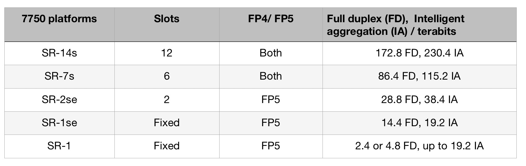
The platforms using the FP5 are the existing 7750 SR-14s and 7750-SR7s routers that were announced with the launch of the FP4.
These chassis were designed to accommodate Nokia’s current and next-generation router cards. “This allows operators to retain the same chassis and support a mix of FP4 and FP5 cards, growing into them gradually,” says Adams.
Nokia has announced three other platforms: two mid-range platforms, the 7750 SR2-se and the 7750 SR1-se, and the 7750 SR-1 that will be available in six variants. “They [the SR-1 boxes] are going to be available in a range of configurations and different port speeds,” says Adams.
Platforms using the FP5 chipset will ship in the first half of 2022, starting with the SR-1.
Nokia also announced an FP5 expandable media adaptor (XMA) line card for the non-fixed platforms (the 7750 SR-14s/ SR-7s and SR-2se). The card supports 36 pluggable slots and with 400 Gigabit Ethernet (GbE) has a capacity of 14.4Tbps full-duplex or 19.2Tbps in intelligent aggregation mode.
The card will also support 400ZR and ZR+ coherent modules and is ready for 800GbE pluggables that will double the card’s capacity ratings.
Nokia says the FP5 improves the throughput of the XMA card by a factor of three: Nokia’s 4.8Tbps XMA (12Tbps IA) uses four FP4 chipsets while the latest 14.4Tbps (19.2Tbps IA) XMA uses six FP5 chipsets.
Custom silicon versus disaggregated designs
Nokia says the benefits of having its own chipset justify the intellectual effort and development expense, even when advanced merchant silicon is available and certain CSPs are embracing open disaggregated routers.
“We feel there is a need in the industry for platforms based on this kind of technology,” says Adams.
What is important is the total cost of ownership and that Nokia’s systems are deployed in critical networks where resiliency, reliability, the feature set and network security are all critical, says Adams.
Nokia also points to the progress it has made since the launch of the FP4. “We have secured 350 projects, two-thirds of which were new footprints or competitive displacements,” says Adams. Nokia’s IP revenues in 2020 were $3.2 billion.
That said, Nokia also partners with merchant silicon vendors: the 7250 IXR interconnect router uses merchant silicon, for example.
“If I look at disaggregation, absolutely, it is an interesting area,” says Adams. “But I think it is very early days.”
Neil McRae, managing director and chief architect at BT, says that while some operators are looking at disaggregated software and hardware, BT doesn’t believe this is necessarily the best solution in terms of performance, reliability or cost.
“Increasingly, the ratio of capital investment in core networking is moving towards optical transceivers than router silicon,” says McRae. “But to get the most out of the network and the router, using custom silicon for the most demanding cases still delivers the best outcomes.
“In our live network but also in our testing, the integrated solution is more reliable, easier to operate and a significant improvement from a total cost of ownership point of view,” says McRae.
BT says it will be able to scale interfaces on the 7750 from 1-400Gbs using the FP5 and Nokia’s SR-OS routing networking software.
BT also highlights the importance of reliability under demand, pointing out how the CSP’s traffic has doubled during the pandemic without impacting its customers.
“Nokia’s understanding of how the underlying silicon is going to react in different situations gives them a significant advantage in building the software on top that performs in challenging situations,” says McRae.
Chip Strategy
Nokia says that were it to sell its FP5 silicon as a standalone product, it would enter a very different design environment.
“You are designing to the requirements of multiple customers versus designing for your systems,” says Adams.
Nokia’s belief is that there is strong demand for platforms designed to purpose.
“We are staying true to that strategy,” says Adams.
Microchip’s compact, low-power 1.6-terabit PHY

Microchip Technology’s latest physical layer (PHY) chip has been developed for next-generation line cards.
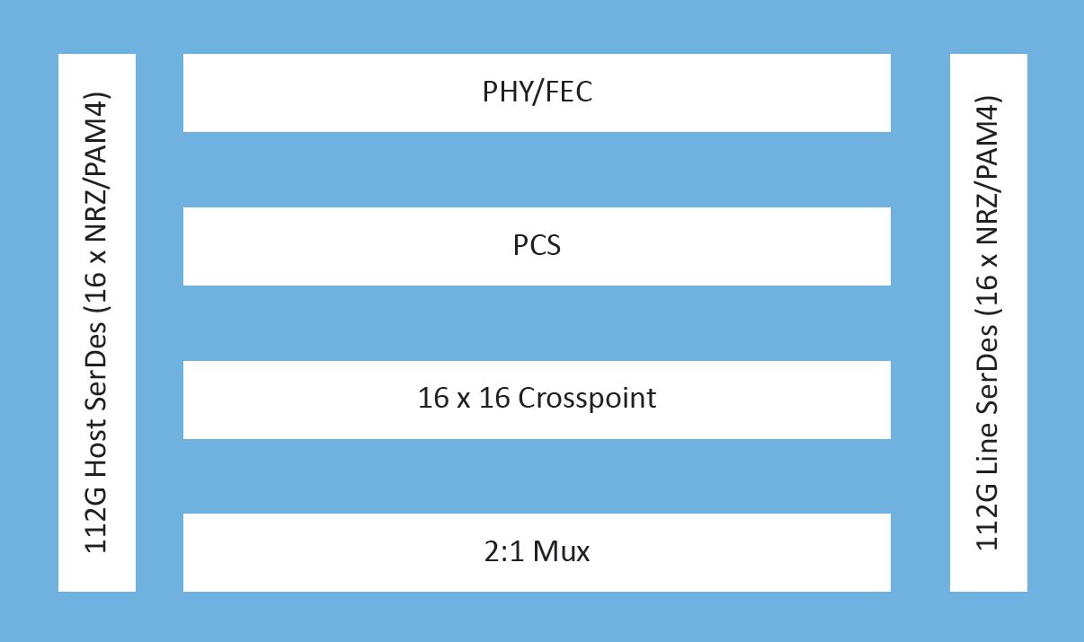
The PM6200 Meta-DX2L (the ‘L’ is for light) 1.6-terabit chip is implemented using TSMC’s 6nm CMOS process. It is Microchip’s first PHY to use 112-gigabit PAM-4 (4-level pulse-amplitude modulation) serialiser/ deserialisers (serdes) interfaces.
Microchip’s existing 16nm CMOS Meta-DX1 PHY devices are rated at 1.2 terabits and use 56-gigabit PAM-4 serdes.
System vendors developing line cards that double the capacity of their switch, router or transport systems are being challenged by space and power constraints, says Microchip. To this aim, the company has streamlined the Meta-DX2L to create a compact, lower-power chip.
“One of the things we have focussed on is the overall footprint of our [IC] design to ensure that people can realise their cards as they go to the 112-gigabit PAM-4 generation,” says Stephen Docking, manager, product marketing, communications business unit, at Microchip.
The company says the resulting package measures 23x30mm and reduces the power per port by 35 per cent compared to the Meta-DX1.
IC architecture
The Meta-DX1 family of 1.2-terabit physical layer (PHY) Ethernet chips effectively comprise three 400-gigabit cores and support the OIF’s Flexible Ethernet (FlexE) protocol and MACsec encryption.
The Meta-DX1 devices, launched in 2019, support the Precision Time Protocol (PTP) used to synchronise clocks across a network with high accuracy that is a requirement for 5G.
The new Meta-DX2L is a single chip although Microchip hints that other family devices will follow.
The Meta-DX2L can be viewed as comprising two 800-gigabit cores. The chip does away with FlexE and the PTP protocol but includes retiming and gearbox modes. The gearbox is used to translate between 28, 56 and 112-gigabit rates.
“We still see customers working on FlexE designs, so the lack of it [with the Meta-DX2L] is not due to limited market demand but how we chose to optimise the chip,” says Docking.
The same applies to PTP. The Meta-DX1 performs time stamping that meets 5G’s Class C and Class D front-haul clocking requirements. “The difference with the Meta-DX2L is that it is not doing time stamping,” says Docking. But it can work with devices doing the time stamping.
“In a 5G system, if you add a PHY, you need to do it in such a way that it doesn’t add any uncertainty in the overall latency of the system,” says Docking. ”So we have focussed on the device have a constant latency.” This means the Meta-DX2L can be used in systems meeting Class C or Class D clocking requirements.
The chip also features a 16×16 crosspoint switch that allows customers to use different types of optical modules and interface them to a line card’s ASIC or digital signal processor (DSP).
The Meta-DX2L’s two cores are flexible and support rates from 1 to 800 Gigabit Ethernet, says Docking.
As well as Ethernet rates, the device supports proprietary rates common with artificial intelligence (AI) and machine learning.
For AI, an array of graphic processor units (GPUs) talk to each other on the same line card. “But to scale the system, you have to have multiple line cards talk to each other,” says Docking. “Different companies that design GPUs have chosen their own protocols to optimise their communications.”
Such links are not aligned with the Ethernet rates but the Meta-DX2L supports these proprietary rates.
Microchip says the Meta-DX2L will sample this quarter.
1.6 terabits, system resilience and design challenges
The PHY’s 1.6-terabit capacity was chosen based on customers’ requirements.
“If you look at the number of ports people want to support, it is often an even multiple of 800-gigabit ports,” says Docking.
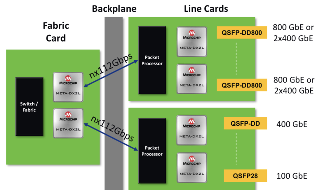
The Meta-DX2L, like its predecessor PHY family, has a hitless 2:1 multiplexer. The multiplexer function is suited for centralised switch platforms where the system intelligence resides on a central card while the connecting line cards are relatively simple, typically comprising PHYs and optical modules.
In such systems, due to the central role of the platform’s switch card, a spare card is included. Should the primary card fail, the backup card kicks in, whereby all the switch’s line cards connect to the backup. The 2:1 multiplexer in the PHY means each line card is interfaced to both switch cards: the primary one and backup.

For line cards that will have 32 or 36 QSFP-DD800 pluggable modules, space is a huge challenge, says Docking: “So having a compact PHY is important.”
“The physical form factor has always been a challenge and then density plays into it and thermal issues,” says Kevin So, associate director, product line management and marketing, communications business unit, at Microchip. “And when you overlay the complexity of the transition from 56 to 112 gigabits, that makes it extremely challenging for board designers.”
Applications
The 1.6-terabit PHY is aimed at switching and routing platforms, compact data centre interconnect systems, optical transport and AI designs.
Which application takes off first depends on several developments. On one side of the PHY chip sits the optics and on the other the ASIC, whether a packet processor, switch chip, processor or DSP. “It’s the timing of those pieces that drive what applications you will see first,” says So.
“Switching and packet processor chips are transitioning to 112-gigabit serdes and you are also starting to see QSFP-DD or OSFP optics with 112-gigabit serdes becoming available,” adds Docking. “So the ecosystem is starting for those types of systems.”
The device is also being aimed at routers for 5G backhaul applications. Here data rates are in the 10- to the 100-gigabit range. “But you are already starting to hear about 400-gigabit rates for some of these access backhaul routers,” says So.
And with 400 Gigabit Ethernet being introduced on access pizza-box routers for 5G this year, in two years, when Microchip’s customers release their hardware, there will likely be denser versions, says So.
“And by then we’ll be talking about a DX3, who knows?” quips So.

The future of optical I/O is more parallel links

Chris Cole has a lofty vantage point regarding how optical interfaces will likely evolve.
As well as being an adviser to the firm II-VI, Cole is Chair of the Continuous Wave-Wavelength Division Multiplexing (CW-WDM) multi-source agreement (MSA).
The CW-WDM MSA recently published its first specification document defining the wavelength grids for emerging applications that require eight, 16 or even 32 optical channels.
And if that wasn’t enough, Cole is also the Co-Chair of the OSFP MSA, which will standardise the OSFP-XD (XD standing for extra dense) 1.6-terabit pluggable form factor that will initially use 16, 100 gigabits-per-second (Gbps) electrical lanes. And when 200Gbps electrical input-output (I/O) technology is developed, OSFP-XD will become a 3.2-terabit module.
Directly interfacing with 100Gbps ASIC serialiser/ deserialiser (serdes) lanes means the 1.6-terabit module can support 51.2-terabit single rack unit (1RU) Ethernet switches without needing 200Gbps ASIC serdes required by eight-lane modules like the OSFP.
“You might argue that it [the OSFP-XD] is just postponing what the CW-WDM MSA is doing,” says Cole. “But I’d argue the opposite: if you fundamentally want to solve problems, you have to go parallel.”
CW-WDM specification
The CW-WDM MSA is tasked with specifying laser sources and the wavelength grids for use by higher wavelength count optical interfaces.
The lasers will operate in a subset of the O-band (1280nm-1320nm) building on work already done by the ITU-T and IEEE standards bodies for datacom optics.
In just over a year since its launch, the MSA has published Revision 1.0 of its technical specification document that defines the eight, 16 and 32 channels.
The importance of specifying the wavelengths is that lasers are the longest lead items, says Cole: “You have to qualify them, and it is expensive to develop more colors.”
In the last year, the MSA has confirmed there is indeed industry consensus regarding the wavelength grids chosen. The MSA has 11 promoter members that helped write the specification document and 35 observer status members.
“The aim was to get as many people on board as possible to make sure we are not doing something stupid,” says Cole.
As well as the wavelengths, the document addresses such issues as total power and wavelength accuracy.
Another issue raised is four-wavelength mixing. As the channel count increases, the wavelengths are spaced closer together. Four-wavelength mixing refers to an undesirable effect that impacts the link’s optical performance. It is a well-known effect in dense WDM transport systems where wavelengths are closely spaced but is less commonly encountered in datacom.
“The first standard is not a link budget specification, which would have included how much penalty you need to allocate, but we did flag the issue,” says Cole. “If we ever publish a link specification, it will include four-wavelength mixing penalty; it is one of those things that must be done correctly.”
Innovation
The MSA’s specification work is incomplete, and this is deliberate, says Cole.
“We are at the beginning of the technology, there are a lot of great ideas, but we are going to resist the temptation to write a complete standard,” he says.
Instead, the MSA will wait to see how the industry develops the technology and how the specification is used. Once there is greater clarity, more specification work will follow.
“It is a tricky balance,” says Cole. “If you don’t do enough, what is the value of it? But if you do too much, you inhibit innovation.”
“The key aspect of the MSA is to help drive compliance in an emerging market,” says Matt Sysak of Ayar Labs and editor of the MSA’s technical specification. “This is not yet standardised, so it is important to have a standard for any new technology, even if it is a loose one.”
The MSA wants to see what people build. “See which one of the grids gain traction,” says Sysak.
Ayar Labs’ SuperNova remote light source for co-packaged optics is one of the first products that is compliant with the CW-WDM MSA.
Sysak notes that at recent conferences co-packaged optics is a hot topic but what is evident is that it is more of a debate.
“The fact that the debate doesn’t seem to coagulate around particular specification definitions and industry standards is indicative of the fact that the entire industry is struggling here,” says Sysak.
This is why the CW-WDM MSA is important, to help promote economies of scale that will advance co-packaged optics.

Applications
Cole notes that, if anything, the industry has become more entrenched in the last year.
The Ethernet community is fixed on four-wavelength module designs. To be able to support such designs as module speeds increase, higher-order modulation schemes and more complex digital signal processors (DSPs) are needed.
“The problem right now is that all the money is going into signal processing: the analogue-to-digital converters and more powerful DSPs,” says Cole.
His belief is that parallelism is the right way to go, both in terms of more wavelengths and more fibers (physical channels).
“This won’t come from Ethernet but emerging applications like machine learning that are not tied to backward compatibility issues,” says Cole. “It is emerging applications that will drive innovation here.”
Cole adds that there is hyperscaler interest in optical channel parallelism. “There is absolutely a groundswell interest here,” says Cole. “This is not their main business right now, but they are looking at their long-term strategy.”
The likelihood is that laser companies will step in to develop the laser sources and then other companies will develop the communications gear.
“It will be driven by requirements of emerging applications,” says Cole. “This is where you will see the first deployments.”
First co-packaged optics switches set for next year
Ranovus says two of its lead customers will deploy co-packaged optics next year.
They will deploy 25.6-terabit Ethernet switch chips but these will be proof-of-concept designs rather than volume deployments.
The deployments will be used to assess the software and gain experience with their maintenance including replacing optics if needed.
“I do think 2024 is going to be the volume year,” says Hamid Arabzadeh, CEO of Ranovus, who expects to announce the customers before the year-end.
Disaggregated server untangles compute, memory and storage elements
Applications
Ranovus is focussed on the emerging integrated optical input-output (I/O) market for Ethernet switches and disaggregated server designs.
A disaggregated server untangles the compute, memory and storage elements found on a server card and pools them separately. This enables a CPU or compute node to access far more memory. It also means each of the server elements can be upgraded independently.
Pooling the memory suits artificial intelligence (AI)/ machine learning applications that process huge data sets. Such applications also require considerable computing.
For machine learning applications, graphic processing unit (GPU) chips are tightly coupled in clusters. But it is a challenge to continually grow the number of GPUs in a cluster and support inter-cluster communications using eletrical interfaces.
Data centre operators want processing performance that scales linearly as more GPUs are adding to a cluster and more clusters are used. This requires longer-reach, high-bandwidth, low-latency links. Limiting the power consumption of such links is also key.
Such system design challenges explain the industry’s interest in adding optical I/O to high-end processors like GPUs. The same applies to Ethernet switch-chips that are doubling in capacity every two years. Moving from electrical to optical interfaces promises longer, energy efficient (measured in pJ/bit), low-latency links.
For Ethernet switch designs, the optical I/O end-point bandwidth needed is at least 3.2 terabits per second (Tbps), says Arabzadeh, whereas for AI it is 0.5-1Tbps.
Odin optical engine
Ranovus recently expanded its optical interconnect portfolio by developing an Odin design that doesn’t need an accompanying retimer chip.
The optical engine combines CMOS and silicon photonics circuits in a monolithic chip, resulting in a smaller, cheaper and power-efficient design.
This second-generation Odin means Ranovus can now offer digital and analogue drive options for co-packaged optics and address more cost-conscious applications such as chip interconnect in servers.
Arabzadeh says its first Odin design that uses a retimer chip helped secure its lead customers.
“We have two lead customers where we are doing the co-packaging of their [switch] chips operating at 100-gigabit PAM-4,” he says. “And we also have an AI customer, where their chip talks PCI Express 5.0 (PCIe 5.0) to our Odin.”
Ranovus first unveiled its Odin-8 800-gigabit design at OFC 2020 and demonstrated it sending eight 100 gigabit PAM-4 (4-level pulse-amplitude modulation) signals, each on a separate fibre.
The design includes a digital retimer IC which takes the OIF-standard extra short reach (XSR) signal – for example, from a switch chip – and recreates (retimes) the PAM-4 signal before forwarding it to Ranovus’ chip. Such a configuration is referred to as a digital-drive design.

“This retimer is not a chip we do and it is expensive,” says Arabzadeh. “It also consumes half the power of the [Odin] chiplet design.”
Ranovus also detailed over a year ago its Odin-32 design that supports four wavelengths per fibre for a total bandwidth of 3.2Tbps.
Since then, Ranovus has developed its Odin-8 for use in an 800-gigabit DR8 optical module. The module will sample and be in the hands of customers for testing in the coming quarter.
The Odin-based 800G-DR8 optical module has a power consumption of 13W; 4W less than rival designs, says Arabzadeh, adding that the optical engine is cost-effective at 400 gigabits, even when using half its capacity.
ODIN version 2.0
The latest monolithic chip is an analogue-drive design. It features radio frequency (RF) drivers, trans-impedance amplifiers (TIAs), silicon photonics transmitters and receivers, and control logic to oversee the components.
The chip does away with clock data recovery (CDR) while integrating the TIAs on-chip. This reduces system costs. “We have the first TIA at 100 gigabits in CMOS,” says Arabzadeh.
To work without the retimer, the monolithic chip is placed much closer to the driving ASIC, with both sharing a common substrate. “It works because it is parked right next to the other chip,” says Arabzadeh.
Ranovus uses a software model of a vendor’s ASIC’s serialiser/ deserialiser (serdes) to ensure the serdes will drive its analogue input.
Being an analogue drive, it is bit-rate and protocol agnostic. “This allows us to get customers beyond the Ethernet market,” says Arabzadeh. These include 100-gigabit PAM-4 signals and the PCIe 5.0 protocol, as mentioned.
For machine learning applications, a proprietary protocol can be used between the end points. NVLink, a serial multi-lane communications link developed by Nvidia, is one such protocol.
Arabzadeh says Ranovus has achieved 1 terabit-per-mm in pitch interface densities: “The stuff we have got involved in with folks in machine learning and AI dwarfs the Ethernet market.”
Laser source
Ranovus’ co-packaged designs use an external laser source. But the company has patented technlogy that allows lasers to be attached directly to the monolithic chip.
This is done at the wafer level, before slicing a wafer to its constituent die. As a result, Ranovus now has two Odin-8 optical engines, one that uses an external laser source (Odin-8ELS) and one with integrated lasers (Odin-8IL)
The laser-attach technology suits optical module designs and expands the company’s optical interconnect toolkit.
The industry has yet to decide whether to adopt a digital or analogue drive approach for co-packaged optics, but the latest Odin design means Ranovus can do both.
Packaging
The company has also been addressing the tricky issue of packaging the chip. “The packaging is a very difficult challenge,” says Arabzadeh.
Ranovus has used the Odin-8 to verify its packaging approach. Two sets of eight fibres are required for the optical I/O (a set to send and a set to receive) and four more fibres are used for the external laser source.
The Odin-32 will use the same packaging and fibre count. What will change is the chip that will support four wavelengths per fibre; instead of the single ring resonator modulator per output, four will be used.
Arabzadeh says each ring modulator is 25 micron so using one or four per path has little impact on the chip’s area.
Market development
Ranovus is addressing both the co-packaged optics and module designs with its Odin designs.
At the OFC conference and exhibition this summer, Arista Networks outlined how pluggable optics will be able to address 102.4 terabit Ethernet switches while Microsoft said it expects to deploy co-packaged optics by the second half of 2024.
Because of the uncertainty as to when co-packaged optics will take off, Ranovus will also supply its optics for the 400-gigabit and 800-gigabit pluggable module market.
“That is why we have yet to tape out the Odin-32,” he says. “We didn’t want to have the technology and there is nobody on the other side of it.”
But the key is to have an optical interface portfolio that secures designs early.
“If you can get the wins and through that, modify your chip, then you are designed in,” says Arabzadeh.

ADTRAN-ADVA's metro-access play

ADTRAN and ADVA have agreed to merge after a long courtship.
The two CEOs have spoken regularly over the years but several developments spurred them to act.
The merger combines ADTRAN’s expertise in access technologies with ADVA’s metro wavelength-division multiplexing (WDM) know-how to create a ‘metro-core-to-door’ company with revenues of $1.2 billion.
ADTRAN and ADVA a better path forward together than separately
As such, the merger promises to double their size and networking skills. Yet the stock market appeared underwhelmed by the announcement, with ADTRAN’s shares down 16% for the rest of the week after the deal was announced.
Market research analysts, however, are more upbeat.
“ADTRAN and ADVA have a better path forward together than separately,” said John Lively, principal analyst at LightCounting Market Research, in a research note.
The deal is expected to close in the second or third quarter of 2022 but only after several hurdles are overcome in what is described as a complex deal.
Motivation
The two companies describe the merger as a logical outcome given recent developments in the marketplace.
“Our combination will make us one of the largest Western suppliers for the markets we serve,” said Tom Stanton, CEO and chairman of ADTRAN, on the call announcing the deal. The word “Western” is noteworthy, reflecting how geopolitics is one catalyst motivating the merger.
The deal will also reposition the two companies with their rivals. ADTRAN will distance itself from broadband competitors such as Calix while ADVA will diversify its business from its current larger competitors, Ciena and Infinera. The new company’s revenues will also approach those of the two players.
The product portfolios of ADTRAN and ADVA have almost no overlap. ADTRAN offers fibre access and connectivity solutions while ADVA addresses metro WDM, data centre interconnect, business Ethernet, network synchronisation and network functions virtualisation (NFV) expertise.
Once combined, each company will seek to expand its sales in the other’s main market.
The US accounts for 74 per cent of ADTRAN’s revenues, while Europe accounts for 21 per cent. Meanwhile, Europe accounts for 62 per cent of ADVA’s business while the US is 29 per cent. The remaining revenues come from the Asia Pacific: ADTRAN, 5 per cent, and ADVA, 9 per cent.
Also cited as a factor is the wave of investment in fibre, not just by communications service providers (CSPs) and public utilities but also government-backed stimulus plans in the US and Europe.
In the US, $66 billion in investment was mentioned spread across programmes such as the infrastructure bill, the second phase of the Rural Digital Opportunity Fund (RDOF), and state-level funding for high-speed broadband.
In Europe, the sum is similar: $35 billion in government funding for high-speed broadband in the European Union, and $30 billion in public and private funding for fibre builds in the UK alone.
“There is an ongoing global fibre investment opportunity that we believe will create sustained momentum for years to come,” said Stanton.
Moreover, having access and second-mile technologies, the new company can better win business. “There is not a customer that we sell to today that, when they are upgrading their access infrastructure, is not also upgrading their middle-mile,” said Stanton.
Becoming a larger player will help, he said: “We see our customers making a significant capital investment to transition their supply chain to trusted vendors.”

Another merger catalyst is the opportunity created by US and European service providers that no longer use Chinese vendors and in some cases are replacing equipment already deployed.
In the US, this is less of an issue due to the fewer deployments while in Europe the process started 18 months ago. Stanton expects Latin America to follow.
“The market opportunity is not just created by all the stimulus but it is also because of the displacement of Eastern vendors,” said Stanton.
There is a land grab going on, he says, and the company that gets there first wins.
“Once you get entrenched in a carrier, regardless of size – the larger ones tend to have two [vendors] and the smaller ones, one – once you are entrenched, it is very difficult to get pulled out,” said Stanton.
Analysis
LightCounting’s view of the merger is positive.
Lively says the merger will not reshape the optical networking industry but it will be attractive to Tier 2 and Tier 3 CSPs that want to buy access and aggregation equipment from a single supplier.
LightCounting notes that the deal values ADVA at $931 million, 1.3x its most recent four quarters of sales.
This is a relatively low valuation: the 2015 Infinera-Transmode merger was 2.6x while the Cisco-Acacia Communications deal, which closed earlier this year, was 7.7x. Of recent deals, only the 2020 Ribbon-ECI Telecom deal was lower, at 1.2x.
LightCounting says one reason for the lower valuation could be ADVA’s port shipments; the vendor is one of the smallest dense WDM suppliers.
The merger’s impact will mostly be felt by the competitors of the existing two companies, says Lively. The new ADTRAN’s sales will be 20 per cent greater than Infinera but still a third of the size of Fiberhome and Ciena.

The importance of size is something both companies stress.
“Our industry has been consolidating and there is an underlying notion that scale matters,” says Stephan Rettenberger, senior vice president, marketing and investor relations at ADVA.
Doubling in size, the new company will be in the same bracket as Infinera while Ciena will be about 3x its size, notes Rettenberger: “The companies that we used to worry about the most are not as distant as before.”
At first glance, the merger between a US and an European company raises questions about the integration challenge. But both firms have American CEOs and both have operations in the US and Germany.
ADTRAN acquired Nokia Siemens Networks’ fixed-line broadband access unit in 2011 while ADVA more recently acquired US firms, MRV Communications and Overture.

Brian Protiva, CEO of ADVA and a co-founder of the company in 1994, is the longest-serving CEO in the optical industry. As such he will have thought long and hard about the deal.
“This business combination is not only about growing the business,” says Protiva. “These two businesses fit perfectly together to address existing market and technology requirements, and we are well-positioned to lead the transition to access and edge convergence.”
Service providers do not need separate infrastructure for business services, residential broadband, and/ or 5G xHauling, he says.
Mechanics
The proposed deal is an all-stock one with ADTRAN and ADVA combining to form ADTRAN Holdings.
Each ADVA share will be swapped for 0.8244 shares of the new company while ADTRAN shares will be exchanged on a one-for-one basis. ADTRAN shareholders will own 54 per cent of the combined company while ADVA shareholders will own 46 per cent, assuming all of the ADVA shares are swapped.
But the new holding company must first be approved by German regulators, expected to occur by November. A three-month offer period then starts during which a minimum of 70 per cent of ADVA shares must be surrendered.
Stanton will continue as CEO and chairman at the new company while ADVA’s Protiva will join as executive vice chairman.
“I’m convinced that Tom is the right person to run the combined company,” says Protiva. “He executes to plan, is well-liked by customers, and thinks very similarly to our ADVA leadership around people first and the customer experience.” Stanton is also a long-serving CEO, heading ADTRAN since 2005.
Protiva will support Stanton during the integration period and then be involved in the corporate strategic direction of ADTRAN, as a board member, using his many long-term relationships in the combined markets.
After that, Protiva says he may return to Egora, a holding company out of which ADVA was born.
ADVA’s CTO, Christoph Glingener, will retain his role with the new company. ADTRAN and ADVA will have a combined annual R&D budget of $250 million.
”The stock exchange offer needs to pass all types of regulatory groups and needs to be accepted by the ADTRAN and ADVA shareholders,” stresses Rettenberger. “There is still a long path to closing.”

Marvell’s latest acquisition: switch-chip firm Innovium

- Innovium will be Marvell’s fifth acquisition in four years
Marvell is buying switch-chip maker, Innovium, for $1.1 billion to bolster its revenues from the lucrative data centre market.
The combination of Innovium with Inphi, Marvell’s most recent $10 billion acquisition, will enable the company to co-package optics alongside the high-bandwidth, low-latency switch chips.
Marvell returns to the market to gain a scalable, low-latency architecture
“Inphi has quite a bit of experience shipping silicon photonics with the ColorZ and ColorZ II [modules],” says Nariman Yousefi, executive vice president, automotive, coherent DSP and switch group at Marvell. “And we have programmes inside the company to do co-packaged optics as well.”
Innovium
Innovium’s Teralynx family addresses the needs of large-scale data centres and will complement Marvell’s Prestera switch-chip portfolio that addresses enterprise and carrier applications.
Formed in 2014, Innovium is a private company with a staff of 230, 185 of which are engaged in R&D. The company has also raised a total of $400 million in funding.
Innovium is already shipping its 12.8-terabit Teralynx 7 to a leading cloud provider and expects revenues of $150 million in 2022. And earlier this year, it announced it shipped over 1 million 400-gigabit switch-silicon ports in 2020.
“The top cloud players are the ones that drive most of the revenues,” says Yousefi. “But there is a long list of customers that are engaged with Innovium at different capacities and there are a bunch of Tier-2s [data centre operators].”
Marvell gained the Xpliant programmable switch-chip architecture for the data centre when it acquired Cavium Networks in 2018, says Devan Adams, principal analyst at LightCounting.
But soon after the acquisition, the Xpliant switch chip line was discontinued as Marvell decided to concentrate on expanding its Prestera chip family.
Now Marvell has returned to the market to gain a scalable, low-latency architecture that addresses the needs of the mega data centre players.
“When you think of the overall data centre market and how it is booming, Innovium makes Marvell’s solutions more attractive to the key cloud customers by helping them expand their switch-chip offerings,” says Adams.

Marvell says it was impressed with the Innovium design team and with the Teralynx architecture when assessing the company as a potential buy. “We also liked the fact that customers have validated the architecture and that it is shipping and in live networks,” says Yousefi.
Broadcom dominates the switch-chip market. According to the market research company, 650 Group, Broadcom had 72 per cent of the 50-gigabit serialiser-deserialiser (serdes) cloud-based switch market in the first quarter, 2021, while Innovium had 27 per cent.
The cloud players want a choice of suppliers, not just for procurement reasons but to ensure sufficiently strong suppliers that can address their needs.
This latest acquisition, expected to close before the year-end, will be Marvell’s fifth acquisition in four years.
Marvell acquired Inphi earlier this year and two custom ASIC companies in 2019: Avera Semiconductor, originally the ASIC group of IBM Microelectronics, and Aquantia that has multi-gigabit PHY expertise. A year before that, Marvell acquired Cavium, as mentioned.
Marvell will use its sales force to promote Innovium’s products to a larger customer base including customers using its Prestera switch chips.
Adams also notes that Marvell has a broad supply chain and a strategic relationship with leading foundry TSMC that will benefit Innovium in the making of its chips, especially when semiconductors are currently in short supply.
Switch chip styles
There are two types of Ethernet switch chips. For the mega data centres, what is important is capacity and the chip’s throughput per Watt (gigabit-per-second/ Watt). Cloud players need to move traffic efficiently in the data centre and with a low latency. Such chips have a streamlined packet-processing capability. Examples include Broadcom’s Tomahawk and Innovium’s Teralynx lines.
In contrast, enterprises need to support various networking protocols and that requires a broad feature set and packet-processing capability. Marvell’s Prestera and Broadcom’s Trident portfolios fall into this category.
“It is hard to design one device that addresses both,” says Yousefi. “That is why there are two different architectures, design teams, databases and chips.”
Marvell highlights Innovium’s Teralynx portfolio’s low power and low latency. “Even though the application for these devices is supposed to be streamlined, Innovium has managed to put in programmability features that makes the architecture more flexible,” says Yousefi. “These are important differentiators.”
Innovium’s Teralynx 8 family includes a 7nm CMOS, 25.6-terabit chip with 112 gigabit-per-second (Gbps) serialisers-deserialisers (serdes). “The Teralynx 8 switch chip is in the bring-up phase with customers; it is not shipping in volume yet,” says Yousefi.
A future Teralynx 9 has also been mentioned.
Yousefi confirms there will be a next-generation 51.2-terabit switch chip and devices beyond that; what the next device will be called is to be determined.
The Marvell acquisition will also combine the serdes expertise of Inphi and Innovium. “We are going to help, but right now we can’t really do much as two separate companies,” says Yousefi.
Integration
Yousefi is also definitive about Marvell’s co-packaged optics plans but points out that the adoption of the technology will take time for the whole industry.
The integration of the Innovium team within Marvell will be fine-tuned once the two companies formally merge. At a high-level, the Innovium team will continue to focus on what it does best: the high-capacity product line, says Yousefi.
“The real opportunity is how do you leverage the collective teams’ knowledge and efficiencies, share the best practices, help each other out during peak resource crunches, and release products more efficiently,” he says.
More acquisitions
The Innovium deal follows the likes of Intel buying Barefoot Networks and Nvidia buying networking specialist Mellanox which designs its own switch chips.
For Adams, it was those deals that suggested it was only a question of time before someone bid for Innovium.
Adams admits he has no insight into Marvell’s acquisition plans, but he points to how Marvell had its own server CPU chip, the ThunderX3 chip based on ARM cores, which was cancelled last year. Could Marvell decide to re-enter the market via the acquisition route?
Another potential technology Marvell could acquire is programmable logic. FPGAs are used in the data centre as accelerators. Adams also points out that certain switch vendors have added FPGAs to their platforms for niche applications such as high-frequency trading.
As for artificial intelligence (AI) hardware, Marvell has its own IP and has added hardware blocks for AI as part of it Octean 10 design. So perhaps the buying of an AI chip start-up is less likely for now.
Yousefi does not rule out more Marvell acquisitions. “The industry is all about growth and how you can position yourself to do many things,” he says.
But he stresses it will take Marvell time to absorb the latest acquisitions of Inphi and Innovium: “That is just as important as acquiring the right assets.”

ADVA’s 800-gigabit CoreChannel causes a stir

ADVA’s latest addition to its FSP 3000 TeraFlex platform provides 800-gigabit optical transmission. But the announcement has caused a kerfuffle among its optical transport rivals.
ADVA’s TeraFlex platform supports various coherent optical transport sleds, a sled being a pluggable modular unit that customises a platform’s functionality.
The coherent sleds use Cisco’s (formerly Acacia Communication’s) AC1200 optical engine. Cisco completed the acquisition of Acacia in March.
The AC1200 comprises a 16nm CMOS Pico coherent digital signal processor (DSP) that supports two wavelengths, each up to 600-gigabit, and two photonic integrated circuits (PICs), for a maximum capacity of 1.2 terabits.
The latest sled from ADVA, dubbed CoreChannel, supports an 800-gigabit stream in a single channel.
ADVA states in its press release that the CoreChannel uses “140 gigabaud (GBd) sub-carrier technology” to deliver 800-gigabit over distances exceeding 1,600km.
This, the company says, improves reach by over 50 per cent compared with state-of-the-art 95GBd symbol rate coherent technologies.
It is these claims that have its rivals reacting.
“Despite their claims – they are not using actual digital sub-carriers,” says one executive from a rival optical transport firm, adding that what ADVA is doing is banding two independent 70GBd 400-gigabit wavelengths together and trying to treat that as a single 800-gigabit signal.
“This isn’t necessarily a bad solution for some applications – each network operator can decide that for themselves,” says the executive. However, he stresses that the CoreChannel is not an 800-gigabit single-channel solution and uses 4th generation 16nm CMOS DSP technology rather than the latest 5th generation, 7nm CMOS DSP technology.
A second executive, from another optical transport vendor providing 800-gigabit single-wavelength solutions, adds that ADVA’s claim of 140GBd is too ‘creative’ for a two-lambda solution.
“It’s not a real 800 gigabit. Not that this must be bad, but one should call things as they are,” the spokesperson said. “What matters to the operators is the cost, power consumption, reach and density of a modem; the number of lambdas is more of an internal feature.”
CoreChannel
ADVA confirms it is indeed using Cisco’s Pico coherent DSP to drive two wavelengths, each at 400 gigabits-per-second (Gbps).
“You can say the CoreChannel is a less challenging requirement because we are not driving it [the Pico DSP] to the maximum modulation or constellation complexity,” says Stephan Rettenberger, senior vice president, marketing and investor relations at ADVA. “It is the lower end of what the AC1200 can do.”
Until now the two wavelengths have been combined externally, and have not been integrated from a software or a command-and-control approach.
“The CoreChannel sled is just another addition to the TeraFlex toolbox,” says Rettenberger. “It has one physical line interface that drives an 800Gbps stream using two wavelengths, each one around 70GBd, that are logically and physically combined.”
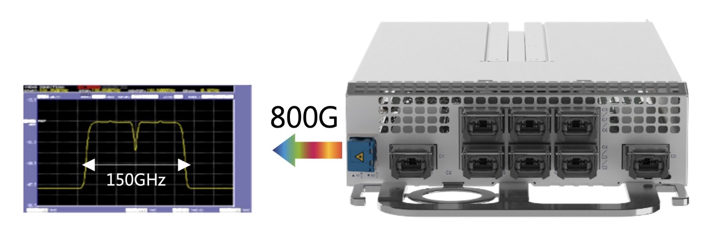
The resulting two-wavelength 800-gigabit stream sits within a 150GHz channel. However, the channel width can be reduced to 125GHz and even 112.5GHz for greater spectral efficiency.
ADVA says the motivation for the design is the customers’ requirement for lower-cost transport and the ability to easily transport 400 Gigabit Ethernet (GbE) client signals.
“With this 800-gigabit line speed, you can go something like 2,000km, that is 50-100 per cent more than what 95GBd single-wavelengths solutions will do,“ says Rettenberger. “And you can also drive it at 400 gigabits and you can do something like 6,000km.”
The reaches quoted are based on a recent field trial involving ADVA.
ADVA uses a single DSP, similar to the latest 800-gigabit systems from Ciena, Huawei and Infinera. Alongside the DSP are two non-hermetically-sealed PICs whereas the 95GBd indium-phosphide solutions use a single hermetically sealed gold box.
ADVA’s solution also requires two lasers whereas the 800-gigabit single-wavelength solutions use one laser.
“Yes, we have two lasers versus one but that is not killing the cost,” says Rettenberger. “And it is also not killing the power consumption because the PIC is so much more power efficient.”
Rettenberger stresses that ADVA is not saying its offering is necessarily a better solution. “But it is a very interesting way to drive 800 gigabits further than these 95 gigabaud solutions,” says Rettenberger. “It has the same cost, space, power efficiency, just greater reach.”
ADVA also agrees that it is not using electrical sub-carriers such as Infinera uses but it is using optical sub-carrier technology.
These two wavelengths are combined logically and also from a physical port interface point of view to fit within a 150GHz window.
The 95GBd, in contrast, is an interim symbol rate step and the resulting 112.5GHz channel width doesn’t easily fit with legacy 25GHz and 50GHz band increments, says ADVA, while the 150GHz band the CoreChannel sled uses is the same channel width that will be used once single-wavelength 140GBd technology becomes available.
Acacia has also long talked about the merit of doubling the baud rate suggesting Cisco’s successor to the AC1200 will have a 140GBd symbol rate. Such a design is expected in the next year or two.
“We feel this [CoreChannel] implementation is already future-proofed,” says Rettenberger.
ADVA says it undertook this development in collaboration with Acacia.
Acacia announced a dual-wavelength single-channel AC1200 solution in 2019. Then, the company unveiled its AC1200-SC2 that delivers 1.2 terabits over an optical channel.
The SC2 (single chip, single channel) is an upgrade of Acacia’s AC1200 module in that it sends 1.2 terabits using two sub-carriers that fit in a 150GHz-wide channel.

Customer considerations
Choosing an optical solution comes down to five factors, each having its weight depending on the network application, says the first executive.
These are capacity-per-wavelength, cost-per-bit, capacity-per- optical-engine or -module, spectral efficiency and hence capacity-per-fibre, and power-per-bit.
“Each is measured for a given distance/ network application,” says the executive. “And the reason the weight changes for different applications is that the importance of each factor is different at different points in the network. For example, the importance of spectral efficiency changes depending on how expensive it is to light up a link (fibre and line system costs).”
For long-haul and submarine, spectral efficiency is the most important factor, while for metro it is typically cost-per-bit. Meanwhile, for data centre interconnect applications, it’s a mix between cost-per-bit and power-per-bit. Capacity-per-wave and capacity-per-optical-engine are valuable because they can reduce the number of wavelengths and modules that need to be deployed, reducing operating expenses and accelerating service activation.
“The reason that 5th generation [7nm CMOS technology] is superior to fourth generation [16nm] DSP technology is that it provides superior performance in every single one of those key criteria,” says the executive. “This fact minimised any potential benefits that could be achieved by banding together two wavelengths using 4th generation technology when compared to a single wavelength using 5th generation technology.”
“It sounds like others feel we have misled the market; that was not the intent,” says Rettenberger.
ADVA does not make its own coherent DSP so it doesn’t care if the chip is implemented using a 16nm, 7nm or a 5nm CMOS process.
“We are trying to build a good solution for transmitting 400GbE signals and, for us, the Pico chip is a wonderful piece of technology that we have now implemented in four different [sled] variants of TeraFlex.”

Turning to optical I/O to open up computing pinch points

Getting data in and out of chips used for modern computing has become a key challenge for designers.
A chip may talk to a neighbouring device in the same platform or to a chip across the data centre.
The sheer quantity of data and the reaches involved – tens or hundreds of meters – is why the industry is turning to optical for a chip’s input-output (I/O).
It is this technology transition that excites Ayar Labs.
The US start-up showcased its latest TeraPHY optical I/O chiplet operating at 1 terabit-per-second (Tbps) during the OFC virtual conference and exhibition held in June.
Evolutionary and revolutionary change
Ayar Labs says two developments are driving optical I/O.
One is the exponential growth in the capacity of Ethernet switch chips used in the data centre. The emergence of 25.6-terabit and soon 51.2-terabit Ethernet switches continue to drive technologies and standards.
This, says Hugo Saleh, vice president of business development and marketing, and recently appointed as the managing director of Ayar Labs’ new UK subsidiary, is an example of evolutionary change.
But artificial intelligence (AI) and high-performance computing have networking needs independent of the Ethernet specification.
“Ethernet is here to stay,” says Saleh. “But we think there is a new class of communications that is required to drive these advanced applications that need low latency and low power.”
Manufacturing processes
Ayar Labs’ TeraPHY chiplet is manufactured using GlobalFoundries’ 45nm RF Silicon on Insulator (45RFSOI) process. But Ayar Labs is also developing TeraPHY silicon using GlobalFoundries’ emerging 45nm CMOS-silicon photonics CLO process (45CLO).
The 45RFSOI process is being used because Ayar Labs is already supplying TeraPHY devices to customers. “They have been going out quite some time,” says Saleh.
But the start-up’s volume production of its chiplets will use GlobalFoundries’ 45CLO silicon photonics process. Version 1.0 of the process design kit (PDK) is expected in early 2022, leading to qualified TeraPHY parts based on the process.
One notable difference between the two processes is that 45RFSOI uses a vertical grating coupler to connect the fibre to the chiplet which requires active alignment. The 45CLO process uses a v-groove structure such that passive alignment can be used, simplifying and speeding up the fibre attachment.
“With high-volume manufacturing – millions and even tens of millions of parts – things like time-in-factory make a big difference,” says Saleh. Every second spent adds cost such that the faster the processes, the more cost-effective and scalable the manufacturing becomes.
Terabit TeraPHY
The TeraPHY chiplet demonstrated during OFC uses eight optical transceivers. Each transceiver comprises eight wavelength-division multiplexed (WDM) channels, each supporting 16 gigabit-per-second (Gbps) of data. The result is a total optical I/O bandwidth of 1.024Tbps operating in each direction (duplex link).
“The demonstration is at 16Gbps and we are going to be driving up to 25Gbps and 32Gbps next,” says Saleh.
The chiplet’s electrical I/O is slower and wider: 16 interfaces, each with 80, 2Gbps channels implementing Intel’s Advanced Interface Bus (AIB) technology.
Last December, Ayar Labs showcased advanced parts using the CLO process. The design was a direct-drive part – a prototype of a future-generation product, not the one demonstrated for OFC.
“The direct-drive part has a serial analogue interface that could come from the host ASIC directly into the ring resonators and modulate them whereas the part we have today is the productised version of an AIB interface with all the macros and all the bandwidth enabled,” says Saleh.
Ayar Labs also demonstrated its 8-laser light source, dubbed SuperNova, that drives the chiplet’s optics.
The eight distributed feedback (DFB) lasers are mixed using a planar lightwave circuit to produce eight channels, each comprising eight frequencies of light.
Saleh compares the SuperNova to a centralised power supply in a server that power pools of CPUs and memory. “The SuperNova mimics that,” he says. “One SuperNova or a 1 rack-unit box of 16 SuperNovas distributing continuous-wave light just like distributed voltage [in a server].”
The current 64-channel SuperNova powers a single TeraPHY but future versions will be able to supply light to two or more.
Ayar Labs is using Macom as its volume supplier of DFB lasers.
Significance
Ayar Labs believes the 1-terabit chip-to-chip WDM link is an industry first.
The demo also highlights how the company is getting closer to a design that can be run in the field. The silicon was made less than a month before the demonstration and was assembled quickly. “It was not behind glass and was operating at room temperature,” says Saleh. “It’s not a lab setting but a production setting.”
The same applies to the SuperNova. The light source is compliant with the Continuous-Wave Wavelength Division Multiplexing (CW-WDM) Multi-Source Agreement (MSA) Group that released its first specification revision to coincide with OFC. The CW-WDM MSA Group has developed a specification for 8, 16, and 32-wavelength optical sources.
The CW-WDM MSA promoter and observer members include all the key laser makers as well as the leading ASIC vendors. “We hope to establish an ecosystem on the laser side but also on the optics,” says Saleh.
“Fundamentally, there is a change at the physical (PHY) level that is required to open up these bottlenecks,” says Saleh. “The CW-WDM MSA is key to doing that; without the MSA you will not get that standardisation.”
Saleh also points to the TeraPHY’s optical I/O’s low power consumption which for each link equates to 5pJ/bit. This is about a tenth of the power consumed by electrical I/O especially when retimers are used. Equally, the reach is up to 2km not tens of centimetres associated with electrical links.
Chiplet demand
At OFC, Arista Networks outlined how pluggable optics will be able to address 102.4 terabit Ethernet switches while Microsoft said it expects to deploy co-packaged optics by the second half of 2024.
Nvidia also discussed how it clusters its graphics processing units (GPUs) that are used for AI applications. However, when a GPU from one cluster needs to talk to a GPU in another cluster, a performance hit occurs.
Nvidia is looking for the optical industry to develop interfaces that will enable its GPU systems to scale while appearing as one tightly coupled cluster. This will require low latency links. Instead of microseconds and milliseconds depending on the number of hops, optical I/O reduces the latency to tens of nanoseconds.
“We spec our chiplet as sub-5ns plus the time of flight which is about 5ns per meter,” says Saleh. Accordingly, the transit time between two GPUs 1m apart is 15ns.
Ayar Labs says that after many conversations with switch vendors and cloud players, the consensus is that Ethernet switches will have to adopt co-packaged optics. There will be different introductory points for the technology but the industry direction is clear.
“You are going to see co-packaged optics for Ethernet by 2024 but you should see the first AI fabric system with co-packaged I/O in 2022,” says Saleh.
Intel published a paper at OFC involving its Stratix 10 FPGA using five Ayar Labs’ chiplets, each one operating at 1.6 terabits (each optical channel operating at 25Gbps, not 16Gbps). The resulting FPGA has an optical I/O capacity of 8Tbps, the design part of the US DARPA PIPES (Photonics in the Package for Extreme Scalability) project.
“A key point of the paper is that Intel is yielding functional units,” says Saleh. The paper also highlighted the packaging and assembly achievements and the custom cooling used.
Intel Capital is a strategic investor in Ayar Labs, as is GlobalFoundries, Lockheed Martin Ventures, and Applied Materials.
Infinera's XR optics pluggable plans

Infinera’s coherent pluggables for XR optics will also address the company’s metro needs.
Coherent pluggables now dominate the metro market where embedded designs account for just a fifth of all ports, says Infinera.
“As we grow our metro business, we need our own pluggables if we want to be cost-competitive,” says Robert Shore, senior vice president of marketing at Infinera.
Infinera’s family of pluggables implementing the XR optics concept is dubbed ICE-XR.
XR optics splits a coherent optical signal into Nyquist sub-carriers, each carrying a data payload. Twenty-five gigabits will likely be the sub-carrier capacity chosen.
XR optics can be used for point-to-point links where all the sub-carriers go to the same destination. But the sub-carriers can also be steered to different destinations, similar to how breakout cables are used in the data centre.
With XR optics, a module can talk to several lower-speed ones in a point-to-multipoint arrangement. This enables optical feeds to be summed, ideal for traffic aggregation applications such as access and 5G.
Open XR Forum
Infinera detailed its ICE-XR pluggables during the OFC virtual conference and exhibition.
The event coincided with the launch of the Open XR Forum whose members include network operators, Verizon, Lumen Technologies (formerly CenturyLink), Windstream and Liberty Global.
Members of the Open XR Forum span sub-component makers, systems vendors like Infinera, and network operators. The day the Open XR Forum website was launched, Infinera received a dozen enquiries from interested parties.
The Open XR Forum will define standards for XR optics such as how the networks are managed, the form factors used, their speeds and power requirements.
“There are a lot of underlying operational aspects that need to be worked out,” says Shore.
XR optics will use a similar model to ZR+ coherent optics. ZR+ delivers enhanced transmission performance compared to the OIF’s 400ZR coherent standard. “ZR+ is not a standard but rather a set of open specifications that can be used by anyone to create a product, and that is exactly the approach we are taking with XR optics,” says Shore.
Over the last 18 months, Infinera has met with 150 network operators regarding XR optics. “We wanted to validate this is a worthwhile technology and that people wanted it,” says Shore.
There have also been 40 network operator trials of the technology by the end of July. BT has used the technology as part of a metro aggregation trial while Virgin Media and American Tower each tested XR optics over PON.
More members have joined the Open XR Forum and will be announced in the autumn.
ICE-XR
ICE-XR’s name combines two concepts.
The first, ICE, refers to the Infinite Capacity Engine, the optics and coherent digital signal processor (DSP) that is the basis for Infinera’s ICE4 and newer ICE6 coherent transmission designs. ICE4 was Infinera’s first product to use Nyquist sub-carriers.
“XR”, meanwhile, borrows from 400ZR. Here, the ‘X’ highlights that XR supports point-to-point coherent communications, like 400ZR, and point-to-multipoint.
“ICE-XR’s release will be timed in conjunction with the official ratification of the specifications from the Open XR Forum,” says Shore.
Infinera’s ICE-XR portfolio will include 100, 400, and 800-gigabit optical modules.
The 100-gigabit ICE-XR, based on four 25-gigabit sub-carriers, will be offered as QSFP-28, QSDP-DD and CFP2 form factors. The 400-gigabit and 800-gigabit variants, using 16 and 32 sub-carriers respectively, will be available as QSFP-DD and CFP2 modules.
The 100-gigabit and 400-gigabit ICE-XR modules will be released first in 2022.
The 400-gigabit ICE-XR will also double as Infinera’s ZR+ offering when used point-to-point.
Shore says its first ZR+ module will not support the oFEC forward-error correction (FEC) used by the OpenZR+ multi-source agreement (MSA).
“The performance hit you take to ensure multi-vendor interoperability is vastly outweighed by the benefits of the improved [optical] performance [using a proprietary FEC],” says Shore.
Merchant DSP suppliers and the systems vendors with in-house DSP designs all support proprietary FEC schemes that deliver far better performance than oFEC, says Shore.
Infinera is developing a monolithic photonic integrated circuit (PIC) for ICE-XR manufactured at its indium phosphide facility.“ICE-XR will increase the utilisation of our fabrication centre, especially when pluggables produce higher volumes compared to embedded [coherent designs],” says Shore.
Infinera says more than one coherent DSP will be needed for the ICE-XR product portfolio. The modules used have a range of power profiles. The QSFP-28 module will need to operate within 4-5W, for example, while the QSFP-DD implementing ZR+ will need to be below 20W. Developing one DSP to span such a power range is not possible.
Business model
The Open XR Forum’s specifications will enable vendors to develop their own XR optics implementations.
Infinera will also license aspects of its design including its coherent DSPs. The aim, says Shore, is to develop as broad an ecosystem as possible: “We want to make XR optics an industry movement.”
Shore stresses ZR+ interoperability is not a must for most applications. Typically, a vendor’s module will be used at both ends of a link to benefit from the ZR+’s custom features. But interoperability is a must for XR optics given its multi-rate nature. The different speed modules from different vendors must talk to each other.
“Because you have multi-generational and multi-rate designs, it becomes even more important to support multi-vendor interoperability,” says Shore. “It gives the network operators more choice, freedom and flexibility.”
XR optics for the data centre
Infinera says there are developments to use XR optics within the data centre.
As data rates between equipment rise, direct-detect optics will struggle to cope, says Shore. The hierarchical architectures used in data centres also lend themselves to a hub-and-spoke architecture of XR optics.
“This type of technology could fit very nicely into that environment once the capacity requirements get high enough,” says Shore.
For this to happen, power-efficient coherent designs are required. But first, XR optics will need to become established and demonstrate a compelling advantage in a point-to-multipoint configuration.
XR optics will also need to replace traditional direct-detect pluggables that continue to progress; 800-gigabit designs are appearing and 1.6-terabit designs were discussed at OFC. Co-packaged optics is another competing technology.
“You are not looking at the 2022-23 timeframe, but maybe 2025-26,” says Shore.
Covid-era shows
Infinera postponed its customer meetings that pre-covid would take place at OFC till after the show to avoid clashing with the online sessions. Once the meetings occurred, customers were given a tour of Infinera’s virtual OFC booth.
Infinera’s solutions marketing team also divided between them the OFC sessions of interest to attend. The team then ‘met’ daily to share their learnings.
“I do think that the world of in-person events has changed forever,” says Shore. Infinera attended 40 events in 2019. “We will probably do fewer than 20 [a year] going forward,” says Shore.