
Building an AI supercomputer using silicon photonics

- Luminous Computing is betting its future on silicon photonics as an enabler for an artificial intelligence (AI) supercomputer
Silicon photonics is now mature enough to be used to design complete systems.
So says Michael Hochberg (pictured), who has been behind four start-ups including Luxtera and Elenion whose products used the technology. Hochberg has also co-authored a book along with Lukas Chrostowski on silicon photonics design.
In the first phase of silicon photonics, from 2000 to 2010, people wondered whether they could even do a design using the technology.
“Almost everything that was being done had to fit into an existing socket that could be served by some other material system,” says Hochberg.
A decade later it was more the case that sockets couldn’t be served without using silicon photonics. “Silicon photonics had dominated every one of the transceiver verticals that matter: intra data centre, data centre interconnect, metro and long haul,” he says.
Now people have started betting their systems using silicon photonics, says Hochberg, citing the examples as lidar, quantum optics, co-packaged optics and biosensing.
Several months ago Hochberg joined as president of Luminous Computing, a start-up that recently came out of stealth mode after raising $105 million in Series A funding.
Luminous is betting its future on silicon photonics as an enabler for an artificial intelligence (AI) supercomputer that it believes will significantly outperform existing platforms.
Machine learning
The vision of AI is to take tasks that were the exclusively the domain of the human mind and automate them at scale, says Hochberg.
Just in the last decade, the AI community has advanced from doing things using machine learning (ML) that are trivial for humans to tasks that only the most talented experts can achieve.
“We have reached the point where machine learning capabilities are superhuman in many respects,” says Hochberg. “Where they produce results quantifiably better than humans can.”
But achieving such machine learning progress has required huge amounts of data and hardware.
“The training runs for the state-of-the-art recommendation engines and natural language models take tens to hundreds of thousands of GPUs (graphics processing units) and they run from months to years,” says Hochberg.
Moreover, the computational demands associated with machine learning training aren’t just doubling every 18 months, like with Moore’s law, but every 3-4 months. “And for memory demands, it is even faster,” he says.
What that means is that the upper limit for doing such training runs are complete data centres.
Luminous Computing wants to develop AI hardware that scales quickly and simply. And a key element of that will be to use silicon photonics to interconnect the hardware.
“One of the central challenges scaling up big clusters is that you have one kind of bus between your CPU and memory, another between your CPU and GPU, another between the GPUs in a box and yet another – Infiniband – between the boxes,” says Hochberg.
These layers of connectivity run at different speeds and latencies that complicate programming for scale. Such systems also result in expensive hardware like GPUs being under-utilised.
“What we are doing is throwing massive optical interconnect at this problem and we are building the system around this optical interconnect,” says Hochberg.
Using sufficient interconnect will enable the computation to scale and will simplify the software. “It is going to be simple to use our system because if you need anything in memory, you just go and get it because there is bandwidth to spare.”
Supercomputing approach
Luminous is not ready to reveal its supercomputer architecture. But the company says it is vertically integrated and is designing the complete system including the processing and interconnect.
When the company started in 2018, it planned to use a photonic processor as the basis of the compute but the class of problems it could solve were deemed insufficiently impactful.
The company then switched to developing a set of ASICs designed around the capabilities of the optics. And it is the optics that rearchitects how data moves within the supercomputer.
“That is the place where you get order-of-magnitude advantages,” says Hochberg.
The architecture will tackle a variety of AI tasks typically undertaken by hyperscalars. “If we can enable them to run models that are bigger than what can be run today while using much smaller programming teams, that has enormous economic impact,” he says.
Hochberg also points out that many organisations want to use machine learning for lots of markets: “They would love to have the ability to train on very large data sets but they don’t have a big distributed systems engineering team to figure out how to scale things up onto big-scale GPUs; that is a market that we want to help.”
The possible customers of Luminous’s system are so keen to access such technology that they are helping Luminous. “That is something I didn’t experience in the optical transceiver world,” quips Hochberg.
The supercomputer will be modular, says Luminous, but its smallest module will have much greater processing capability than, say, a platform hosting 8 or 16 GPUs.
Silicon photonics
Luminous is confident in using silicon photonics to realise its system even though the design will advance how the technology has been used till now.
“You are always making a bet in this space that you can do something that is more complex than anything anyone else is doing because you are going to ship your product a couple of years hence,” says Hochberg
Luminous is has confidence because of the experience of its design team, the design tools it has developed and its understanding of advanced manufacturing processes.
“We have people that know how to stand up complex things,” says Hochberg.
Status
Luminous’s staff is currently around 100, a doubling in the last year. And it is set to double again by year-end.
The company is busy doing modelling work as to how the machine learning algorithms will run on its system. “Not just today’s models but also tomorrow’s models,” says Hochberg.
Meanwhile, there is a huge amount of work to be done to deliver the first hardware by 2024.
“We have a bunch of big complex chips we have to build, we have software that has to live on top of it, and it all has to come together and work,” concludes Hochberg.

Can a think tank tackle telecoms innovation deficit?
The Telecom Ecosystem Group (TEG) will publish shortly its final paper that concludes two years of industry discussion on ways to spur innovation in telecommunications.
The paper, entitled Addressing the Telecom Innovation Deficit, says telcos have lost much of their influence in shaping the technologies on which they depend.
“They have become ageing monocultures; disruptive innovators have left the industry and innovation is outsourced,” says the report.
The TEG has held three colloquiums and numerous discussion groups soliciting views from experienced individuals across the industry during the two years.
The latest paper names eight authors but many more contributed to the document and its recommendations.
Network transformation
Don Clarke, formerly of BT and CableLabs, is one of the authors of the latest paper. He also co-authored ETSI’s Network Functions Virtualisation (NFV) paper that kickstarted the telcos’ network transformation strategies of the last decade.
Many of the changes sought in the original NFV paper have come to pass.
Networking functions now run as software and no longer require custom platforms. To do that, the operators have embraced open interfaces that allow disaggregated designs to tackle vendor lock-in. The telcos have also adopted open-source software practices and spurred the development of white boxes to expand equipment choice.
Yet the TEG paper laments the industry’s continued reliance on large vendors while smaller telecom vendors – seen as vital to generate much-needed competition and innovation – struggle to get a look-in.
The telecom ecosystem
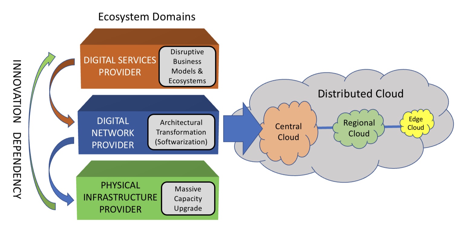
The TEG segments the telecommunications ecosystem into three domains (see diagram).
The large-scale data centre players are the digital services providers (top layer). In this domain, innovation and competition are greatest.
The digital network provider domain (middle layer) is served by a variety of players, notably the cloud providers, while it is the telcos that dominate the physical infrastructure provider domain.
At this bottom layer, competition is low and overall investment in infrastructure is inadequate. A third of the world’s population still has no access to the internet, notes the report.
The telcos should also be exploiting the synergies between the domains, says the TEG, yet struggle to do so. But more than that, the telcos can be a barrier.
Clarke cites the emerging metaverse that will support immersive virtual worlds as an example.
Metaverse
The “Metaverse” is a concept being promoted by the likes of Meta and Microsoft and has been picked up by the telcos, as evident at this week’s MWC Barcelona 22 show.
Meta’s Mark Zuckerberg recently encouraged his staff to focus on long-term thinking as the company transitions to become a metaverse player. “We should take on the challenges that will be the most impactful, even if the full results won’t be seen for years,” he said.
Telcos should be thinking about how to create a network that enables the metaverse, given the data for rendering metaverse environments will come through the telecom network, says Clarke.

“The real innovation will come when you try and understand the needs of the metaverse in terms of networking, and then you get into the telco game,” he says.
Any concentration of metaverse users will generate a data demand likely to exhaust the network capacity available.
“Telcos will say, ‘We aren’t upgrading capacity because we are not getting a return,’ and then metaverse innovation will be slowed down,” says Clarke.
He says much of the innovation needed for the metaverse will be in the network and telcos need to understand the opportunities for them. “The key is what role will the telcos have, not in dollars but network capability, then you start to see where the innovation needs to be done.”
The challenge is that the telcos can’t see beyond their immediate operational challenges, says Clarke: “Anything new creates more operational challenges and therefore needs to be rejected because they don’t have the resources to do anything meaningful.”
He stresses he is full of admiration for telcos’ operations staff: “They know their game.” But in an environment where operational challenges are avoided, innovation is less important.
TEG’s action plan
TEG’s report lists direct actions telcos can take regarding innovation. These cover funding, innovation processes, procurement and increasing competition.
Many of the proposals are designed to help smaller vendors overcome the challenges they face in telecoms. TEG views small vendors and start-ups as vital for the industry to increase competition and innovation.
Under the funding category, TEG wants telcos to allocate a least 5 per cent of procurement to start-ups and small vendors. The group also calls for investment funds to be set up that back infrastructure and middleware vendors, not just over-the-top start-ups.
For innovation, it wants greater disaggregation so as to steer away from monolithic solutions. The group also wants commitments to fast lab-to-field trials (a year) and shorter deployment cycles (two years maximum) of new technologies.
Competition will require a rethink regarding small vendors. At present, all the advantages are with the large vendors. It lists six measures how telcos can help small vendors win business, one being to stop forcing them to partner with large vendors. The TEG wants telcos to ensure enough personnel that small vendors get all the “airtime” they need with the telcos.
Lastly, concerning procurement, telcos can do much more.
One suggestion is to stop sending small vendors large, complex request for proposals (RFPs) that they must respond to in short timescales; small vendors can’t compete with the large RFP teams available to the large vendors.
Also, telcos should stop their harsh negotiating terms such as a 30 per cent additional discount. Such demands can hobble a small vendor.
Innovation
“Innovation comes from left field and if you try to direct it with a telco mindset, you miss it,” says Clarke. “Telcos think they know what ‘good’ looks like when it comes to innovation, but they don’t because they come at it from a monoculture mindset.”
He said that in the TEG discussions, the idea of incubators for start-ups was mentioned. “We have all done incubators,” he says. But success has been limited for the reasons cited above.
He also laments the lack of visionaries in the telecom industry.
A monoculture organisation rejects such individuals. “Telcos don’t like visionaries because culturally they are annoying and they make their life harder,” he says. “Disruptors have left the industry.”
Prospects
The authors are realistic.
Even if their report is taken seriously, they note any change will take time. They also do not expect the industry to be able to effect change without help. The TEG wants government and regulator involvement if the long-term prospects of a crucial industry are to be ensured.
The key is to create an environment that nurtures innovation and here telcos could work collectively to make that happen.
“No telco has it all, but individual ones have strengths,” says Clarke. “If you could somehow combine the strengths of the particular telcos and create such an environment, things will emerge.”
The trick is diversity – get people from different domains together to make judgements as to what promising innovation looks like.
“Bring together the best people and marvelous things happen when you give them a few beers and tell them to solve a problem impacting all of them,” says Clarke. “How can we make that happen?”

The various paths to co-packaged optics

Near package optics has emerged as companies have encountered the complexities of co-packaged optics. It should not be viewed as an alternative to co-packaged optics but rather a pragmatic approach for its implementation.
Co-packaged optics will be one of several hot topics at the upcoming OFC show in March.
Placing optics next to silicon is seen as the only way to meet the future input-output (I/O) requirements of ICs such as Ethernet switches and high-end processors.
For now, pluggable optics do the job of routing traffic between Ethernet switch chips in the data centre. The pluggable modules sit on the switch platform’s front panel at the edge of the printed circuit board (PCB) hosting the switch chip.
But with switch silicon capacity doubling every two years, engineers are being challenged to get data into and out of the chip while ensuring power consumption does not rise.
One way to boost I/O and reduce power is to use on-board optics, bringing the optics onto the PCB nearer the switch chip to shorten the electrical traces linking the two.
The Consortium of On-Board Optics (COBO), set up in 2015, has developed specifications to ensure interoperability between on-board optics products from different vendors.
However, the industry has favoured a shorter still link distance, coupling the optics and ASIC in one package. Such co-packaging is tricky which explains why yet another approach has emerged: near package optics.
I/O bottleneck
“Everyone is looking for tighter and tighter integration between a switch ASIC, or ‘XPU’ chip, and the optics,” says Brad Booth, president at COBO and principal engineer, Azure hardware architecture at Microsoft. XPU is the generic term for an IC such as a CPU, a graphics processing unit (GPU) or even a data processing unit (DPU).
What kick-started interest in co-packaged optics was the desire to reduce power consumption and cost, says Booth. These remain important considerations but the biggest concern is getting sufficient bandwidth on and off these chips.
“The volume of high-speed signalling is constrained by the beachfront available to us,” he says.
Booth cites the example of a 16-lane PCI Express bus that requires 64 electrical traces for data alone, not including the power and ground signalling. “I can do that with two fibres,” says Booth.

Near package optics
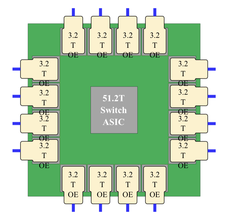
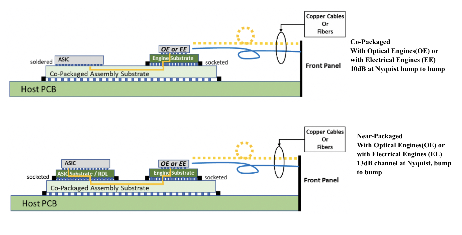
With co-packaged optics, the switch chip is typically surrounded by 16 optical modules, all placed on an organic substrate (see diagram below).
“Another name for it is a multi-chip module,” says Nhat Nguyen, senior director, solutions architecture at optical I/O specialist, Ayar Labs.
A 25.6-terabit Ethernet switch chip requires 16, 1.6 terabits-per-second (1.6Tbps) optical modules while upcoming 51.2-terabit switch chips will use 3.2Tbps modules.
“The issue is that the multi-chip module can only be so large,” says Nguyen. “It is challenging with today’s technology to surround the 51.2-terabit ASIC with 16 optical modules.”
Near package optics tackles this by using a high-performance PCB substrate – an interposer – that sits on the host board, in contrast to co-packaged optics where the modules surround the chip on a multi-chip module substrate.
The near package optics’ interposer is more spacious, making the signal routing between the chip and optical modules easier while still meeting signal integrity requirements. Using the interposer means the whole PCB doesn’t need upgrading which would be extremely costly.
Some co-packaged optics design will use components from multiple suppliers. One concern is how to service a failed optical engine when testing the design before deployment. “That is one reason why a connector-based solution is being proposed,” says Booth. “And that also impacts the size of the substrate.”
A larger substrate is also needed to support both electrical and optical interfaces from the switch chip.
Platforms will not become all-optical immediately and direct-attached copper cabling will continue to be used in the data centre. However, the issue with electrical signalling, as mentioned, is it needs more space than fibre.
“We are in a transitional phase: we are not 100 per cent optics, we are not 100 per cent electrical anymore,” says Booth. “How do you make that transition and still build these systems?”
Perspectives
Ayar Labs views near package optics as akin to COBO. “It’s an attempt to bring COBO much closer to the ASIC,” says Hugo Saleh, senior vice president of commercial operations and managing director of Ayar Labs U.K.
However, COBO’s president, Booth, stresses that near package optics is different from COBO’s on-board optics work.
“The big difference is that COBO uses a PCB motherboard to do the connection whereas near package optics uses a substrate,” he says. “It is closer than where COBO can go.”
It means that with near package optics, there is no high-speed data bandwidth going through the PCB.
Booth says near package optics came about once it became obvious that the latest 51.2-terabit designs – the silicon, optics and the interfaces between them – cannot fit on even the largest organic substrates.
“It was beyond the current manufacturing capabilities,” says Booth. “That was the feedback that came back to Microsoft and Facebook (Meta) as part of our Joint Development Foundation.”
Near package optics is thus a pragmatic solution to an engineering challenge, says Booth. The larger substrate remains a form of co-packaging but it has been given a distinct name to highlight that it is different to the early-version approach.
Nathan Tracy, TE Connectivity and the OIF’s vice president of marketing, admits he is frustrated that the industry is using two terms since co-packaged optics and near package optics achieve the same thing. “It’s just a slight difference in implementation,” says Tracy.
The OIF is an industry forum studying the applications and technology issues of co-packaging and this month published its framework Implementation Agreement (IA) document.
COBO is another organisation working on specifications for co-packaged optics, focussing on connectivity issues.
Technical differences
Ayar Labs highlights the power penalty using near package optics due to its use of longer channel lengths.
For near package optics, lengths between the ASIC and optics can be up to 150mm with the channel loss constrained to 13dB. This is why the OIF is developing the XSR+ electrical interface, to expand the XSR’s reach for near package optics.
In contrast, co-packaged optics confines the modules and host ASIC to 50mm of each other. “The channel loss here is limited to 10dB,” says Nguyen. Co-packaged optics has a lower power consumption because of the shorter spans and 3dB saving.
Ayar Labs highlights its optical engine technology, the TeraPHY chiplet that combines silicon photonics and electronics in one die. The optical module surrounding the ASIC in a co-packaged design typically comprises three chips: the DSP, electrical interface and photonics.
“We can place the chiplet very close to the ASIC,” says Nguyen. The distance between the ASIC and the chiplet can be as close as 3-5mm. Whether on the same interposer Ayar Labs refers to such a design using athird term: in-package optics.
Ayar Labs says its chiplet can also be used for optical modules as part of a co-packaged design.
The very short distances using the chiplet result in a power efficiency of 5pJ/bit whereas that of an optical module is 15pJ/bit. Using TeraPHY for an optical module co-packaged design, the power efficiency is some 7.5pJ/bit, half that of a 3-chip module.
A 3-5mm distance also reduces the latency while the bandwidth density of the chiplet, measured in Gigabit/s/mm, is higher than the optical module.
Co-existence
Booth refers to near package optics as ‘CPO Gen-1’, the first generation of co-packaged optics.
“In essence, you have got to use technologies you have in hand to be able to build something,” says Booth. “Especially in the timeline that we want to demonstrate the technology.”
Is Microsoft backing near package optics?

“We are definitely saying yes if this is what it takes to get the first level of specifications developed,” says Booth.
But that does not mean the first products will be exclusively near package optics.
“Both will be available and around the same time,” says Booth. “There will be near packaged optics solutions that will be multi-vendor and there will be more vertically-integrated designs; like Broadcom, Intel and others can do.”
From an end-user perspective, a multi-vendor capability is desirable, says Booth.
Ayar Labs’ Saleh sees two developing paths.
The first is optical I/O to connect chips in a mesh or as part of memory semantic designs used for high-performance computing and machine learning. Here, the highest bandwidth and lowest power are key design goals.
Ayar Labs has just announced a strategic partnership with high performance computing leader, HPE, to design future silicon photonics solutions for HPE’s Slingshot interconnect that is used for upcoming Exascale supercomputers and also in the data centre.
The second path concerns Ethernet switch chips and here Saleh expects both solutions to co-exist: near package optics will be an interim solution with co-packaged optics dominating longer term. “This will move more slowly as there needs to be interoperability and a wide set of suppliers,” says Saleh.
Booth expects continual design improvements to co-packaged optics. Further out, 2.5D and 3D chip packaging techniques, where silicon is stacked vertically, to be used as part of co-packaged optics designs, he says.

Infinera’s ICE6 crosses the 100-gigabaud threshold

Coherent discourse 3
- The ICE6 Turbo can send two 800-gigabit wavelengths over network spans of 1,100-1,200km using a 100.4 gigabaud (GBd) symbol rate.
- The enhanced reach can reduce the optical transport equipment needed in a network by 25 to 30 per cent.
Infinera has enhanced the optical performance of its ICE6 coherent engine, increasing by up to 30 per cent the reach of its highest-capacity wavelength transmissions.
The ICE6 Turbo coherent optical engine can send 800-gigabit optical wavelengths over 1,100-1,200km compared to the ICE6’s reach of 700-800km.
ICE6 Turbo uses the same coherent digital signal processor (DSP) and optics as the ICE6 but operates at a higher symbol rate of 100.4GBd.
“This is the first time 800 gigabits can hit long-haul distances,” says Ron Johnson, general manager of Infinera’s optical systems & network solutions group.
Baud rates
Infinera’s ICE6 operates at 84-96GBd to transmit two wavelengths ranging from 200-800 gigabits. This gives a total capacity of 1.6 terabits, able to send 4×400 Gigabit Ethernet (GbE) or 16x100GbE channels, for example.
Infinera’s ICE6’s coherent DSP uses sub-carriers and their number and baud rates are tuned to the higher symbol rate.
The bit rate sent is defined using long-codeword probabilistic constellation shaping (LC-PAS) while Infinera also uses soft-decision FEC gain sharing between the DSP’s two channels.
The ICE6 Turbo adds several more operating modes to the DSP that exploit this higher baud rate, says Rob Shore, senior vice president of marketing at Infinera.
Reach
Infinera says that the ICE6 Turbo can also send two 600-gigabit wavelengths over 4,000km.

“This is almost every network in the world except sub-sea,” says Shore, adding that the enhanced reach will reduce the optical transport equipment needed in a network by 25 to 30 per cent.
“One thousand kilometres sending 2×800 gigabits or 4x400GbE is a powerful thing,” adds Johnson. “We’ll see a lot of traction with the content providers with this.”
Increasing symbol rate
Optical transport system designers continue to push the symbol rate. Acacia, part of Cisco, has announced its next 128GBd coherent engine while Infinera’s ICE6 Turbo now exceeds 100GBd.
Increasing the baud rate boosts the capacity of a single coherent transceiver while lowering the cost and power used to transport data. A higher baud rate can also send the same data further, as with the ICE6 Turbo.
“The original ICE6 device was targeted for 84GBd but it had that much overhead in the design to allow for these higher baud rate modes,” says Johnson. “We strived for 84GBd and technically we can go well beyond 100.4GBd.”
This is common, he adds.
The electronics of the coherent design – the silicon germanium modulator drivers, trans-impedance amplifiers, and analogue-to-digital and digital-to-analogue converters – are designed to perform at a certain level and are typically pushed harder and harder over time.
Baud rate versus parallel-channel designs
Shore believes that the industry is fast approaching the point where upping the symbol rate will no longer make sense. Instead, coherent engines will embrace parallel-channel designs.
Already upping the baud rate no longer improves spectral efficiency. “The industry has lost a vector in which we typically expect improvements generation by generation,” says Shore. “We now only have the vector of lowering cost-per-bit.”
At some point, coherent designs will use multiple DSP cores and wavelengths. What matters will be the capacity of the optical engine rather than the capacity of an individual wavelength, says Shore.
“We have had a lot of discussion about parallelism versus baud rate,” adds Johnson.
Already there is fragmentation with embedded and pluggable coherent optics designs. Embedded designs are optimised for high-performance spectral efficiency while for pluggables cost-per-bit is key.
This highlights that there is more than one optimisation approach, says Johnson: “We have got to develop multiple technologies to hit all those different optimisations.”
Infinera will use 5nm and 3nm CMOS for its future coherent DSPs, optimised for different parts of the network.
Infinera will keep pushing the baud rate but Johnson admits that at some point the cost-per-bit will start to rise.
“At present, it is not clear that doubling the baud rate again is the right answer,” says Johnson. “Maybe it is a combination of a little bit more [symbol rate] and parallelism, or it is moving to 200GBd.”
The key is to explore the options and deliver coherent technology consistently.
“If we put too much risk in one area and drive too hard, it has the potential to push our time-to-market out,” says Johnson.
The ICE6 Turbo will be showcased at the OFC show being held in San Diego in March.

Building the data rate out of smaller baud rates

In the second article addressing the challenges of increasing the symbol rate of coherent optical transport systems, Professor Andrew Lord, BT’s head of optical network research, argues that the time is fast approaching to consider alternative approaches.
Coherent discourse 2
Coherent optical transport systems have advanced considerably in the last decade to cope with the relentless growth of internet traffic.
One-hundred-gigabit wavelengths, long the networking standard, have been replaced by 400-gigabit ones while state-of-the-art networks now use 800 gigabits.
Increasing the data carried by a single wavelength requires advancing the coherent digital signal processor (DSP), electronics and optics.
It also requires faster symbol rates.
Moving from 32 to 64 to 96 gigabaud (GBd) has increased the capacity of coherent transceivers from 100 to 800 gigabits.
Last year, Acacia, now part of Cisco, announced the first 1-terabit-plus wavelength coherent modem that uses a 128GBd symbol rate.
Other vendors will also be detailing their terabit coherent designs, perhaps as soon as the OFC show, to be held in San Diego in March.
The industry consensus is that 240GBd systems will be possible towards the end of this decade although all admit that achieving this target is a huge challenge.
Baud rate
Upping the baud rate delivers several benefits.
A higher baud rate increases the capacity of a single coherent transceiver while lowering the cost and power used to transport data. Simply put, operators get more bits for the buck by upgrading their coherent modems.
But some voices in the industry question the relentless pursuit of higher baud rates. One is Professor Andrew Lord, head of optical network research at BT.
“Higher baud rate isn’t necessarily a panacea,” says Lord. “There is probably a stopping point where there are other ways to crack this problem.”
Parallelism
Lord, who took part in a workshop at ECOC 2021 addressing whether 200+ GBd transmission systems are feasible, says he used his talk to get people to think about this continual thirst for higher and higher baud rates.
“I was asking the community, ‘Are you pushing this high baud rate because it is a competition to see who builds the biggest rate?’ because there are other ways of doing this,” says Lord.
One such approach is to adopt a parallel design, integrating two channels into a transceiver instead of pushing a single channel’s symbol rate.
“What is wrong with putting two lasers next to each other in my pluggable?” says Lord. “Why do I have to have one? Is that much cheaper?”
For an operator, what matters is the capacity rather than how that capacity is achieved.
Lord also argues that having a pluggable with two lasers gives an operator flexibility.
A single-laser transceiver can only go in one direction but with two, networking is possible. “The baud rate stops that, it’s just one laser so I can’t do any of that anymore,” says Lord.
The point is being reached, he says, where having two lasers, each at 100GBd, probably runs better than a single laser at 200GBd.
Excess capacity
Lord cites other issues arising from the use of ever-faster symbol rates.
What about links that don’t require the kind of capacity offered by very high baud rate transceivers?
If the link spans a short distance, it may be possibe to use a higher modulation scheme such as 32-ary quadrature amplitude modulation (32-QAM) or even 64-QAM. With a 200GBd symbol rate transceiver, that equates to a 3.2-terabit transceiver. “Yet what if I only need 100 gigabits,” says Lord.
One option is to turn down the data rate using, say, probabilistic constellation shaping. But then the high-symbol rate would still require a 200GHz channel. Baud rate equals spectrum, says Lord, and that would be wasting the fibre’s valuable spectrum.
Another solution would be to insert a different transceiver but that causes sparing issues for the operators.
Alternatively, the baud rate could be turned down. “But would operators do that?” says Lord. “If I buy a device capable of 200GBd, wouldn’t I always operate it at its maximum or would I turn it down because I want to save spectrum in some places?”
Turning the baud rate down also requires the freed spectrum to be used and that is an optical network management challenge.
“If I need to have to think about defragmenting the network, I don’t think operators will be very keen to do that,” says Lord.
Pushing electronics
Lord raises another challenge: the coherent DSP’s analogue-to-digital and digital-to-analogue converters.
Operating at a 200+ GBd symbol rate means the analogue-to-digital converters at the coherent receiver must operate at least at 200 giga-samples per second.
“You have to start sampling incredibly fast and that sampling doesn’t work very well,” says Lord. “It’s just hard to make the electronics work together and there will be penalties.”
Lord cites research work at UCL that suggests that the limitations of the electronics – and the converters in particular – are not negligible. Just connecting two transponders over a short piece of fibre shows a penalty.
“There shouldn’t be any penalty but there will be, and the higher the baud rate, you will get a penalty back-to-back because the electronics are not perfect,” he says.
He suspects the penalty is of the order of 1 or 2dB. That is a penalty lost to the system margin of the link before the optical transmission even starts.
Such loss is clearly unacceptable especially when considering how hard engineers are working to enhance algorithms for even a few tenths of a dB gain.
Lord expects that such compromised back-to-back performance will ultimately lead to the use of multiple adjacent carriers.
“Advertising the highest baudrate is obviously good for publicity and shows industry leadership,” he concludes. “But it does feel that we are approaching a limit for this, and then the way forward will be to build aggregate data rates out of smaller baud rates.”
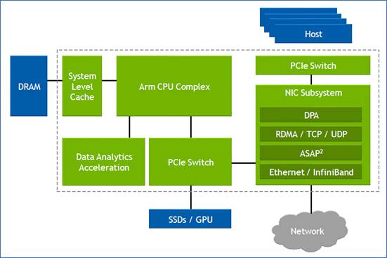
Nvidia's plans for the data processor unit
When Nvidia’s CEO, Jensen Huang, discussed its latest 400-gigabit BlueField-3 data processing unit (DPU) at the company’s 2021 GTC event, he also detailed its successor.
Companies rarely discuss chip specifications two generations ahead; the BlueField-3 only begins sampling next quarter.
The BlueField-4 will advance Nvidia’s DPU family.
It will double again the traffic throughput to 800 gigabits-per-second (Gbps) and almost quadruple the BlueField-3’s integer processing performance.
But one metric cited stood out. The BlueField-4 will increase by nearly 1000x the number of terabit operators-per-second (TOPS) performed: 1,000 TOPS compared to the BlueField-3’s 1.5 TOPS.
Huang said artificial intelligence (AI) technologies will be added to the BlueField-4, implying that the massively parallel hardware used for Nvidia’s graphics processor units (GPUs) are to be grafted onto its next-but-one DPU.
Why add AI acceleration? And will it change the DPU, a relatively new processor class?
Data processor units
Nvidia defines the DPU as a programmable device for networking.
The chip combines general-purpose processing – multiple RISC cores used for control-plane tasks and programmed in a high-level language – with accelerator units tailored for packet-processing data-plane tasks.
“The accelerators perform functions for software-defined networking, software-defined storage and software-defined security,” says Kevin Deierling, senior vice president of networking at Nvidia.
The DPU can be added to a Smart Network Interface Card (SmartNIC) that complements the server’s CPU, taking over the data-intensive tasks that would otherwise burden the server’s most valuable resource.
Other customers use the DPU as a standalone device. “There is no CPU in their systems,” says Deierling.
Storage platforms is one such example, what Deierling describes as a narrowly-defined workload. “They don’t need a CPU and all its cores, what they need is the acceleration capabilities built into the DPU, and a relatively small amount of compute to perform the control-path operations,” says Deierling.
Since the DPU is the server’s networking gateway, it supports PCI Express (PCIe). The PCIe bus interfaces to the host CPU, to accelerators such as GPUs, and supports NVMe storage. NVMe is a non-volatile memory host controller interface specification.
BlueField 3
When announced in 2021, the 22-billion transistor BlueField-3 chip was scheduled to sample this quarter. “We need to get the silicon back and do some testing and validation before we are sampling,” says Deierling.
The device is a scaled-up version of the BlueField-2: it doubles the throughput to 400Gbps and includes more CPU cores: 16 Cortex-A78 64-bit ARM cores.
Nvidia deliberately chose not to use more powerful ARM cores. “The ARM is important, there is no doubt about it, and there are newer classes of ARM,” says Deierling. “We looked at the power and the performance benefits you’d get by moving to one of the newer classes and it doesn’t buy us what we need.”
The BlueField-3 has the equivalent processing performance of 300 X86 CPU cores, says Nvidia, but this is due mainly to the accelerator units, not the ARM cores.
The BlueField-3 input-output [I/O] includes Nvidia’s ConnectX-7 networking unit that supports 400 Gigabit Ethernet (GbE) which can be split over 1, 2 or 4 ports. The DPU also doubles the InfiniBand interface compared to the BlueField-2, either a single 400Gbps (NDR) port or two 200Gbps (HDR) ports. There are also 32 lanes of PCI Express 5.0, each lane supporting 32 giga-transfers-per-second (GT/s) in each direction.
The memory interface is two DDR5 channels, doubling both the memory performance and the channel count of the BlueField-2.
The data path accelerator (DPA) of the BlueField-3 comprises 16 cores, each supporting 16 instruction threads. Typically, when a packet arrives, it is decrypted and the headers are inspected after which the accelerators are used. The threads are used if the specific function needed is not accelerated. Then, a packet is assigned to a thread and processed.
“The DPA is a specialised part of our acceleration core that is highlighly programmable,” says Deierling.
Other programmable logic blocks include the accelerated switching and packet processing (ASAP2) engine that parses packets. It inspects packet fields looking for a match that tells it what to do, such as dropping the packet or rewriting its header.
In-line acceleration
The BlueField-3 implements the important task of security.
A packet can have many fields and encapsulations. For example, the fields can include a TCP header, quality of service, a destination IP and an IP header. These can be encapsulated into an overlay such as VXLAN and further encapsulated into a UDP packet before being wrapped in an outer IP datagram that is encrypted and sent over the network. Then, only the IPSec header is exposed; the remaining fields are encrypted.
Deierling says the BlueField-3 does the packet encryption and decryption in-line.
For example, the DPU uses the in-line IPsec decode to expose the headers of the various virtual network interfaces – the overlays – of a received packet. Picking the required overlay, the packet is sent to a set of service-function chainings that use all the accelerators available such as tackling distributed denial-of-service and implementing a firewall and load balancing.
“You can do storage, you can do an overlay, receive-side scaling [RSS], checksums,” says Deierling. “All the accelerations built into the DPU become available.”
Without in-line processing, the received packet goes through a NIC and into the memory of the host CPU. There, it is encrypted and hence opaque; the packet’s fields can’t benefit from the various acceleration techniques. “It is already in memory when it is decrypted,” says Deierling.
Often, with the DPU, the received packet is decrypted and passed to the host CPU where the full packet is visible. Then, once the host application has processed the data, the data and packet may be encrypted again before being sent on.
“In a ‘zero-trust’ environment, there may be a requirement to re-encrypt the data before sending it onto the next hop,” says Deierling. “In this case, we just reverse the pipeline.”
An example is confidential healthcare information where data needs to be encrypted before being sent and stored.
DPU evolution
There are many application set to benefit from DPU hardware. These cover the many segments Nvidia is addressing including AI, virtual worlds, robotics, self-driving cars, 5G and healthcare.
All need networking, storage and security. “Those are the three things we do but it is software-defined and hardware-accelerated,” says Deierling.
Nvidia has an ambitious target of launching a new DPU every 18 months. That suggests the BlueField-4 could sample as early as the end of 2023.
The 800-gigabit Bluefield-4 will have 64-billion transistors and nearly quadruple the integer processing performance of the BlueField-3: from 42 to 160 SPECint.
Nvidia says its DPUs, including the BlueField-4, are evolutionary in how they scale the ARM cores, accelerators and throughput. However, the AI acceleration hardware added to the BlueField-4 will change the nature of the DPU.
“What is truly salient is that [1,000] TOPS number,” says Deierling. “And that is an AI acceleration; that is leveraging capabilities Nvidia has on the GPU side.”
Self-driving cars, 5G and robotics
An AI-assisted DPU will support such tasks as video analytics, 5G and robotics.
For self-driving cars, the DPU will reside in the data centre, not in the car. But that too will change.“Frankly, the car is becoming a data centre,” notes Deierling.
Deep learning currently takes place in the data centre but as the automotive industry adopts Ethernet, a car’s sensors – lidar, radar and cameras – will send massive amounts of data which an IC must comprehend.
This is relevant not just for automotive but all applications where data from multiple sensors needs to be understood.
Deierling describes Nvidia as an AI-on-5G company.
“We have a ton of different things that we are doing and for that, you need a ton of parallel-processing capabilities,” he says. This is why the BlueField-4 is massively expanding its TOPS rating.
He describes how a robot on an automated factory floor will eventually understand its human colleagues.
“It is going to recognize you as a human being,“ says Deierling. “You are going to tell it: ‘Hey, stand back, I’m coming in to look at this thing’, and the robot will need to respond in real-time.”
Video analytics, voice processing, and natural language processing are all needed while the device will also be running a 5G interface. Here, the DPU will reside in a small mobile box: the robot.
“Our view of 5G is thus more comprehensive than just a fast pipe that you can use with a virtual RAN [radio access network] and Open RAN,” says Deierling. “We are looking at integrating this [BlueField-4] into higher-level platforms.”

Huawei sets transmission record with new modulator

Coherent discourse: Part 1
A paper from Huawei and Sun Yat-Sen University in the January issue of the Optica journal describes a thin-film lithium niobate modulator. The modulator enabled a world-record coherent optical transmission, sending nearly 2 terabits of data over a single wavelength.
Much of the industry’s focus in recent years has been to fit coherent optical technology within a pluggable module.
Such pluggables allow 400-gigabit coherent interfaces to be added to IP routers and switches, serving the needs of the data centre operators and telecom operators.
But research labs of the leading optical transport vendors continue to advance high-end coherent systems beyond 800-gigabit-per-wavelength transmissions.
Optical transport systems from Ciena, Infinera and Huawei can send 800-gigabit wavelengths using a symbol rate of 96-100 gigabaud (GBd).
Acacia Communications, part of Cisco, detailed late last year the first 1.2-terabit single-wavelength coherent pluggable transceiver that will operate at 140GBd, twice the symbol rate of 400-gigabit modules such as 400ZR.
Now Huawei has demonstrated in the lab a thin-film lithium niobate modulator that supports a symbol rate of 220GBd and beyond.
Maxim Kuschnerov, director of the optical and quantum communications laboratory at Huawei, says the modulator has a 110GHz 3dB bandwidth but that it can be operated at higher frequencies, suggesting a symbol rate as high as 240GBd.
Thin-film lithium niobate modulator
Huawei says research is taking place into new materials besides the established materials of indium phosphide and silicon photonics. “It is a very exciting topic lately,” says Kuschnerov.
He views the demonstrated thin-film lithium niobate optical modulator as disruptive: “It can cover up several deficiencies of today’s modulators.”
Besides the substantial increase in bandwidth – the objective of any new coherent technology – the modulator has performance metrics that benefit the coherent system such as a low driving voltage and low insertion loss.
A driving voltage of a modulator is a key performance parameter. For the modulator, it is sub-1V.
The signal driving the modulator comes from a digital-to-analogue (D/A) converter, part of the coherent digital signal processor (DSP). The D/A output is fed into a modulator driver. “That [driver] requires power, footprint, and increases the complexity of integrating the [modem’s] modules tighter,” says Kuschnerov.
The modulator’s sub-1V drive voltage is sufficiently small that the DSP’s CMOS-based D/A can drive it directly, removing the modulator driver circuit that also has bandwidth performance limitations. The modulator thus reduces the transmitter’s overall cost.
The low-loss modulator also improves the overall optical link budget. And for certain applications, it could even make the difference as to whether optical amplification is needed.
“The modulator checks the box of very high bandwidth,” says Kuschnerov. “And it helps by not having to add a semiconductor optical amplifier for some applications, nor needing a driver amplifier.”
One issue with the thin-film modulator is its relative size. While not large – it has a length of 23.5mm – it is larger than indium phosphide and silicon photonics modulators.
1.96-terabit wavelength
Huawei’s lab set-up used a transmit coherent DSP with D/As operating at 130 Giga-samples-per-second (GS/s) to drive the modulator. The modulation used was a 400-quadrature amplitude modulation (400-QAM) constellation coupled with probabilistic constellation shaping.
A 10 per cent forward error correction scheme was used such that, overall, 1.96-terabits per second of data was sent using a single wavelength.
The D/A converter was implemented in silicon germanium using high-end lab equipment to generate the signal at 130GS/s.
“This experiment shows how much we still need to go,” says Kuschnerov. “What we have done at 130GBd shows there is a clear limitation with the D/A [compared to the 220GBd modulator].”
Baud-rate benefits
Increasing the baud rate of systems is not the only approach but is the favoured implementation choice.
What customers want is more capacity and reducing the cost per bit for the same power consumption. Increasing the baud rate decreases the cost and power consumption of the optical transceiver.
By doubling the baud rate, an optical transceiver delivers twice the capacity for a given modulation scheme. The cost per bit of the transceiver decreases as does the power consumed per bit. Instead of two transceivers and two sets of components, one transceiver and one set are used instead.
But doubling the baud rate doesn’t improve the optical system’s spectral efficiency since doubling the baud rate doubles the channel width. That said, algorithmic enhancements are added to each new generation of coherent modem but technically, the spectral efficiency practically no longer improves.
Huawei acknowledges that while the modulator promises many benefits, all the coherent modem’s components – the coherent ASIC, the D/A and analogue-to-digital (D/A) converters, the optics, and the analogue circuitry – must equally scale. This represents a significant challenge.
Kuschnerov says optical research is finding disruptive answers but scaling performance, especially on the electrical side, remains a critical issue. “How do you increase the D/A sampling rates to match these kinds of modulator technologies?” he says. “It is not straightforward.”
The same is true for the other electrical components: the driver technologies and the trans-impedance amplifier circuits at the receiver.
Another issue is combining the electrical and optical components into a working system. Doubling the signalling of today’s optical systems is a huge radio frequency design and packaging challenge.
But the industry consensus is that with newer CMOS processes and development in components and materials, doubling the symbol rate again to 240GB will be possible.
But companies don’t know – at least they are not saying – what the upper symbol rate limit will be. The consensus is that increasing the baud rate will end. Then, other approaches will be pursued.
Kuschnerov notes that if a 1.6-terabit transceiver could be implemented using a single wavelength or with eight 200Gbps ones with the same spectral performance, cost, footprint and power consumption, end users wouldn’t care which of the two were used.
However, does optics enable such greater parallelism?
Kuschnerov says that while decades of investment has gone into silicon photonics, it is still not there yet.
“It doesn’t have the cost-effectiveness at 16, 32 or 64 lanes because the yield goes down significantly,” he says. “We as an industry can’t do it yet.”
He is confident that, soon enough, the industry will figure out how to scale the optics: “With each generation, we are getting better at it.”
Coherent engineers will then have more design options to meet the system objectives.
And just like with microprocessors, it will no longer be upping the clock frequency but rather adopting parallel processing i.e. multiple cores. Except, in this case, it will be parallel coherent optics.

Books read in 2021: Final Part

In the final favoured reads during 2021, the contributors are Daryl Inniss of OFS, Vladimir Kozlov of LightCounting Market Research, and Gazettabyte’s editor.
Daryl Inniss, Director, Business Development at OFS
Four thousand weeks is the average human lifetime.
A book by Oliver Burkeman: Four Thousand Weeks: Time Management For Mortals is a guide to using the finite duration of our lives.
Burkeman argues that by ignoring the reality of our limited lifetime, we fill our lives with busyness and distractions and fail to achieve the very fullness that we seek.
While sobering, Burkeman presents thought-provoking and amusing examples and stories while transitioning them into positive action.
An example is his argument that our lives are insignificant and that, regardless of our accomplishments, the universe continues unperturbed. Setting unrealistic goals is one consequence of our attempt to achieve greatness.
On the other hand, recognising our inability to transform the world should give us enormous freedom to focus on the things we can accomplish.
We can jettison that meaningless job, be fearless in the face of pandemics given that they come and go throughout history, and lower our stresses on financial concerns given they are transitory. What is then left is the freedom to spend time on things that do matter to us.
Defining what’s important is an individual thing. It need not be curing cancer or solving world peace – two of my favourites. It can be something as simple as making a most delicious cookie that your kids enjoy.
It is up to each of us to find those items that make us feel good and make a difference. Burkeman guides us to pursue a level of discomfort as we seek these goals.
I found this book profound and valuable as I enter the final stage of my life.
I continue to search for ways to fulfil my life. This book helps me to reflect and consider how to use my finite time.
Vladimir Kozlov, CEO and Founder of LightCounting Market Research
Intelligence is a fascinating topic. The artificial kind is making all the headlines but alien minds created by nature have yet to be explored.
One of the most bizarre among these is the distributed mind of the octopus. “Other Minds: The Octopus, the Sea and the Deep Origins of Consciousness, by Peter Godfery-Smith, is a perfect introduction to the subject.
The Overstory: A Novel, by Richard Powers takes the concept of alien minds to a new, more emotional level. It is a heavy read. The number of characters rivals that of War and Peace while the density matches the style of Dostoevsky. Yet, it is impossible not to finish the book, even if it takes several months.
It concerns the conflict of “alien minds”. The majority of the aliens are humans, cast from the distant fringes of our world. The trees emerge as a unifying force that keeps the book and the planet together. It is an unforgettable drama.
I have not cut a live tree since reading the book. I can not stop thinking about just how shallow our understanding of the world is.
The intelligence created by nature is more puzzling than dark matter yet it is shuffled into the ‘Does-not-matter’ drawer of our alien minds.
Roy Rubenstein, Gazettabyte’s editor
Ten per cent of my contacts changed jobs in 2021, according to LinkedIn.
Of these, how many quit their careers after 32 years at one firm? And deliberately downgraded their salaries?
That is what Kate Kellaway did. The celebrated Financial Times journalist quit her job to become a school teacher.
Kellaway is also a co-founder of Now Teach, a non-profit organisation that helps turn experienced workers in such professions as banking and the law into teachers.
In her book, Re-educated: How I Changed My Job, My Home and My Hair, Kellaway reflects on her career as a journalist and on her life. She notes how privileged she has been in the support she received that helped her correct for mistakes and fulfill her career; something that isn’t available to many of her students.
She also highlights the many challenges of teaching. In one chapter she describes a class and the exchanges with her students that captures this magnificently.

A book I reread after many years was Arthur Miller’s autobiography, Timebends: A Life.
In the mid-1980s on a trip to the UK to promote his book, Miller visited the Royal Exchange Theatre in Manchester. There, I got a signed copy of his book which I prize.
The book starts with his early years in New York, surrounded by eccentric Jewish relatives.
Miller also discusses the political atmosphere during the 1950s, resulting in his being summoned before the House Un-American Activities Committee. The first time I read this, that turbulent period seemed very much a part of history. This time, the reading felt less alien.
Miller is fascinating when explaining the origins of his plays. He also had an acute understanding of human nature, as you would expect of a playwright.
The book I most enjoyed in 2021 is The Power of Strangers: The Benefits of Connecting in a Suspicious World, by Joe Keohane.
The book explores talking to strangers and highlights a variety of people going about it in original ways.
Keohane describes his many interactions that include an immersive 3-day course on how to talk to strangers, held in London, and a train journey between Chicago and Los Angeles; the thinking being that, during a 42-hour trip, what else would you do but interact with strangers.
Keohane learns that, as he improves, there is something infectious about the skill: people start to strike up conversations with him.
The book conveys how interacting with strangers can be life-enriching and can dismantle long-seated fears and preconceptions.
He describes an organisation that gets Republican and Democrat supporters to talk. At the end of one event, an attendee says: “We’re all relieved that we can actually talk to each other. And we can actually convince the other side to look at something a different way on some subjects.”
If reading novels can be viewed as broadening one’s experiences through the stories of others, then talking to strangers is the non-fiction equivalent.
I loved the book.
Intel sets a course for scalable optical input-output

- Intel is working with several universities to create building-block circuits to address its optical input-output (I/O) needs for the next decade-plus.
- By 2024 the company wants to demonstrate the technologies achieving 4 terabits-per-second (Tbps) over a fibre at 0.25 picojoules-per-bit (pJ/b).
Intel has teamed up with seven universities to address the optical I/0 needs for several generations of upcoming products.
The initiative, dubbed the Intel Research Center for Integrated Photonics for Data Centre Interconnects, began six months ago and is a three-year project.
No new location is involved, rather the research centre is virtual with Intel funding the research. By setting up the centre, Intel’s goal is to foster collaboration between the research groups.
Motivation
James Jaussi, senior principal engineer and director of the PHY Research Lab in Intel Labs, (pictured) heads a research team that focuses on chip-to-chip communication involving electrical and optical interfaces.
“My team is primarily focussed on optical communications, taking that technology and bringing it close to high-value silicon,” says Jaussi.
Much of Jaussi’s 20 years at Intel has focussed on electrical I/O. During that time, the end of electrical interfaces has repeatedly been predicted. But copper’s demise has proved overly pessimistic, he says, given the advances made in packaging and printed circuit board (PCB) materials.
But now the limits of copper’s bandwidth and reach are evident and Intel’s research arm wants to ensure that when the transition to optical occurs, the technology has longevity.
“This initiative intends to prolong the [optical I/O] technology so that it has multiple generations of scalability,” says Jaussi. And by a generation, Jaussi means the 3-4 years it takes typically to double the bandwidth of an I/O specification.
Co-packaged optics and optical I/O
Jaussi distinguishes between co-packaged optics and optical I/O.
He describes co-packaged optics as surrounding a switch chip with optics. Given the importance of switch chips in the data centre, it is key to maintain compatibility with specifications, primarily Ethernet.
But that impacts the power consumption of co-packaged optics. “The power envelope you are going to target for co-packaged optics is not necessarily going to meet the needs of what we refer to as optical I/O,” says Jaussi.
Optical I/O involves bringing the optics closer to ICs such as CPUs and graphics processor units (GPUs). Here, the optical I/O need not be aligned with standards.
The aim is to take the core I/O off a CPU or GPU and replace it with optical I/O, says Jaussi.
With optical I/O, non-return-to-zero (NRZ) signalling can be used rather than 4-level pulse amplitude modulation (PAM-4). The data rates are slower using NRZ but multiple optical wavelengths can be used in parallel. “You can power-optimise more efficiently,” says Jaussi.
Ultimately, co-packaged optics and optical I/O will become “stitched together” in some way, he says.
Research directions
One of the research projects involves the work of Professor John Bowers and his team at the University of California, Santa Barbara, on the heterogeneous integration of next-generation lasers based on quantum-dot technology.
Intel’s silicon photonics transceiver products use hybrid silicon quantum well lasers from an earlier collaboration with Professor Bowers.
The research centre work is to enable scalability by using multi-wavelength designs as well as enhancing the laser’s temperature performance to above 100oC. This greater resilience to temperature helps the laser’s integration alongside high-performance silicon.
Another project, that of Professor Arka Majumdar at the University of Washington, is to develop non-volatile reconfigurable optical switching using silicon photonics.
“We view this as a core building block, a capability,” says Jaussi. The switching element will have a low optical loss and will require liitle energy for its control.
The switch being developed is not meant to be a system but an elemental building block, analogous to a transistor, Intel says, with the research exploring the materials needed to make such a device.
The work of Professor S.J. Ben Yoo at University of California, Davis, is another of the projects.
His team is developing a silicon photonics-based modulator and a photodetector technology to enable 40-terabit transceivers at 150fJ/bit and achieving 16Tb/s/mm I/O density.
“The intent is to show over a few fibres a massive amount of bandwidth,” says Jaussi.
Goals
Intel says each research group has its own research targets that will be tracked.
All the device developments will be needed to enable the building of something far more sophisticated in future, says Jaussi.
At Intel Labs’ day last year, the company spoke about achieving 1Tbps of I/O at 1pJ/s. The research centre’s goals are more ambitious: 4Tbps over a fibre at 0.25pJ/b in the coming three years.
There will be prototype demonstrations showing data transmissions over a fibre or even several fibres. “This will allow us to make that scalable not just for one but two, four, 10, 20, 100 fibres,” he says. “That is where that parallel scalability will come from.”
Intel says it will be years before this technology is used for products but the research goals are aggressive and will set the company’s optical I/O goals.

PCI-SIG releases the next PCI Express bus specification

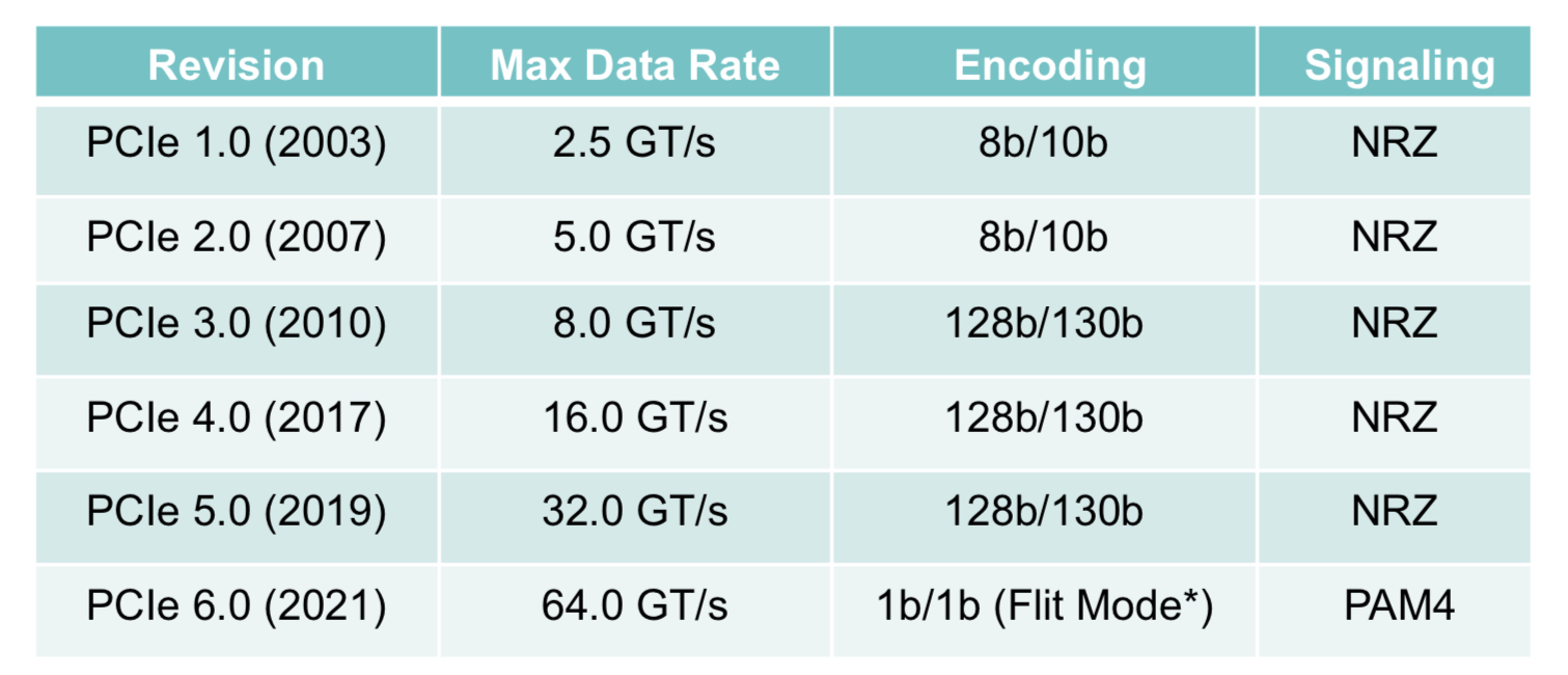
The Peripheral Component Interconnect Express (PCIe) 6.0 specification doubles the data rate to deliver 64 giga-transfers-per-second (GT/s) per lane.
For a 16-lane configuration, the resulting bidirectional data transfer capacity is 256 gigabytes-per-second (GBps).
“We’ve doubled the I/O bandwidth in two and a half years, and the average pace is now under three years,” says Al Yanes, President of the Peripheral Component Interconnect – Special Interest Group (PCI-SIG).
The significance of the specification’s release is that PCI-SIG members can now plan their products.
Users of FPGA-based accelerators, for example, will know that in 12-18 months there will be motherboards running at such rates, says Yanes
Applications
The PCIe bus is used widely for such applications as storage, processors, artificial intelligence (AI), the Internet of Things (IoT), mobile, and automotive.
In servers, PCIe has been adopted for storage and by general-purpose processors and specialist devices such as FPGAs, graphics processor units (GPUs) and AI hardware.
The CXL standard enables server disaggregation by interconnecting processors, accelerator devices, memory, and switching, with the protocol sitting on top of the PCIe physical layer. The NVM Express (NVMe) storage standard similarly uses PCIe.
“If you are on those platforms, you know you have a healthy roadmap; this technology has legs,” says Yanes.
A focus area for PCI-SIG is automotive which accounts for the recent membership growth; the organisation now has 900 members. PCI-SIG has also created a new workgroup addressing automotive.
Yanes attributes the automotive industry’s interest in PCIe due to the need for bandwidth and real-time analysis within cars. Advanced driver assistance systems, for example, use a variety of sensors and technologies such as AI.
PCIe 6.0
The PCIe bus uses a dual simplex scheme – serial transmissions in both directions – referred to as a lane. The bus can be configured in several lane configurations: x1, x2, x4, x8, x12, x16 and x32, although x2, x12 and x32 are rarely used.
PCIe 6.0’s 64GT/s per lane is double that of PCIe 5.0 that is already emerging in ICs and products.
IBM’s latest 7nm POWER10 16-core processor, for example, uses the PCIe 5.0 bus as part of its I/O, while the latest data processing units (DPUs) from Marvell (Octeon 10) and Nvidia (BlueField 3) also support PCIe 5.0.
To achieve the 64GT/s transfer rates, the PCIe bus has adopted 4-level pulse amplitude modulation (PAM-4) signalling. This requires forward error correction (FEC) to offset the bit error rates of PAM-4 while minimising the impact on latency. And low latency is key given the PCIe PHY layer is used by such protocols as CXL that carry coherency and memory traffic. (see IEEE Micro article.)
The latest specification also adopts flow control unit (FLIT) encoding. Here, fixed 256-byte packets are sent: 236 bytes of data and 20 bytes of cyclic redundancy check (CRC).
Using fixed-length packets simplifies the encoding, says Yanes. Since the PCIe 3.0 specification, 128b/130b encoding has been used for clock recovery and the aligning of data. Now with the fixed-sized packet of FLIT, no encoding bits are needed. “They know where the data starts and where it ends,” says Yanes.
Silicon designed for PCIe 6.0 will also be able to use FLITs with earlier standard PCIe transfer speeds.
Yanes says power-saving modes have been added with the release. Both ends of a link can agree to make lanes inactive when they are not being used.
Status and developments
IP blocks for PCIe 6.0 already exist while demonstrations and technology validations will occur this year. First products using PCIe 6.0 will appear in 2023.
Yanes expects PCIe 6.0 to be used first in servers with accelerators used for AI and machine learning, and also where 800 Gigabit Ethernet will be needed.
PCI-SIG is also working to develop new cabling for PCIe 5.0 and PCIe 6.0 for sectors such as automotive. This will aid the technology’s adoption, he says
Meanwhile, work has begun on PCIe 7.0.
“I would be ecstatic if we can double the data rate to 128GT/s in two and a half years,” says Yanes. “We will be investigating that in the next couple of months.”
One challenge with the PCIe standard is that it borrows the underlying technology from telecom and datacom. But the transfer rates it uses are higher than the equivalent rates used in telecom and datacom.
So, while PCI 6.0 has adopted 64GT/s, the equivalent rate used in telecom is 56Gbps only. The same will apply if PCI-SIG chooses 128GT/s as the next data rate given that telecom uses 112Gbps.
Yanes notes, however, that telecom requires much greater reaches whereas PCIe runs on motherboards, albeit ones using advanced printed circuit board (PCB) materials.