Optical interconnect specialist Ayar Labs has announced that it is working with Nvidia, a leader in artificial intelligence (AI) and machine learning silicon, systems and software.
In February Ayar Labs announced a strategic collaboration with the world’s leading high-performance computing (HPC) firm, Hewlett Packard Enterprise (HPE).
Both Nvidia and HPE were part of the Series C funding worth $130 million that Ayar Labs secured in April.
Work partnerships
Ayar Labs has chiplet and external laser source technologies that enable optical input-output (I/O) suited for AI and high-performance computing markets.
Charles Wuischpard, CEO of Ayar Labs, says the work with HPE and Nvidia share common characteristics.
HPE is interested in optical interfaces for high-performance computing fabrics and, in particular, future generations of its Slingshot technology.
Nvidia is also interested in fabrics with its Mellanox technology, but its chips also impact the server. Wuishchpard describes its work with Nvidia as optically enabling Nvidia’s NVLink, its graphics processing unit (GPU) interface.
Nvidia’s optical needs
Bill Dally, chief scientist and senior vice president of research at Nvidia, outlined the company’s interest in optical interconnect at the OFC conference, held in San Diego in March.
Dally started by quantifying the hierarchy of bandwidths and power requirements when sending a bit in computing systems.
The maximum bandwidth and lowest power needs occur, not surprisingly, when data is sent on-chip, between the chip’s processing elements.
With each hierarchical connection jump after that – between chips on an interposer hosting, for example, GPUs and memory (referred to as a module), between modules hosted on a printed circuit board (PCB), linking the boards in a cabinet, and connecting cabinets in a cluster – the bandwidth drops (dubbed bandwidth tapering) and more power is needed to transmit a bit.
There are also different technologies used for the jumps: electrical traces connect the modules on the PCB; electrical cables link the boards in a cabinet (1m to 3m), while active optical cables link the cabinets (5m to 100m).
One issue is that electrical signalling is no longer getting faster (the FO4 delay metric is now constant) with each new CMOS process node. Another issue is that the electrical reach is shrinking with each signalling speed hike: 50-gigabit signals can span 3m, while 200-gigabit signals can span 1m.
Co-packaged optics, where optics are placed next to the IC, promises the best of both worlds: bettering the metrics of PCBs and electrical cable while matching the reach of active optical cables.
Co-packaged optics promises a 5x saving in power when sending a bit compared to a PCB trace while costing a tenth of an active optical cable yet matching its 100m reach. Co-packaged optics also promises a fourfold increase in density (bit/s/mm) compared to PCB traces, says Nvidia.
However, meeting these targets requires overcoming several challenges.
One is generating efficient lasers that deliver aligned frequency grids. Another is getting the micro-ring resonators, used for modulating the data over WDM links, to work reliably and in volume. Nvidia plans to use 8 or 16 micro-ring resonators per WDM link and has developed five generations of test chips that it is still evaluating.
Another issue is packaging the optics, reducing the optical loss when coupling the fibre to the GPU while avoiding the need for active alignment. Cost is a big unknown, says Dally, and if co-packaged optics proves significantly more costly than an electrical cable, it will be a non-starter.
Nvidia outlined an example optical link using 8- or 16-channel WDM links, each channel at 25 gigabit-per-second (Gbps), to enable 200 and 400-gigabit optical links.
Using two polarisations, 800-gigabit links are possible while upgrading each lambda to 50Gbps, and link speed doubles again to 1.6 terabits.
Implementing such links while meeting the cost, power, density and reach requirements is why Nvidia has invested in and is working with Ayar Labs.
“Nvidia has been keeping an eye on us for some time, and they are generally big believers in a micro-ring WDM-based architecture with a remote light source,” says Wuishchpard.
Nvidia is optimistic about overcoming the challenges and that in the coming years – it won’t say how many – it expects electrical signalling to be used only for power. At the same time, co-packaged optics will handle the interconnect.
Nvidia detailed a conceptual GPU architecture using co-packaged optics.
Each GPU would be co-packaged with two optical engines, and two GPUs would sit on a card. Eight or nine cards would fill a chassis and eight to 10 chassis a cabinet.
Each GPU cabinet would then connect to a switch cabinet which would host multiple switch chips, each switch IC co-packaged with six optical engines.
The resulting cluster would have 4,000 to 8,000 GPUs, delivering a ‘flat bandwidth taper’.
HPE’s roadmap
Ayar Labs is collaborating with HPE to develop optical interconnect technology for high-performance computing while jointly developing an ecosystem for the technology.
Marten Terpstra
“This is not just a component that you stick on, and your product becomes better and cheaper,” says Marten Terpstra, senior director of product management and high-performance networks at HPE. “This is a change in architecture.”
HPE is interested in Ayar Labs’ optical interconnect chiplets and lasers for upcoming generations of its Slingshot interconnect technology used for its ‘Shasta ‘ HPE Cray EX and other platforms.
The increase in signalling speeds from 50 to 100 gigabits and soon 200 gigabits is making the design of products more complicated and expensive in terms of cost, power and cooling.
“This [optical interconnect] is something you need to prepare for several years in advance,” says Terpstra. “It is a shift in how you create connectivity, an architectural change that takes time.”
Shasta architecture
HPE’s Slingshot interconnect is part of the liquid-cooled Shasta and a top-of-rack switch for air-cooled HPE Cray supercomputers and HPC clusters.
“There are two parts to Slingshot: the Rosetta chipset which sits inside the switch, and the Cassini chipset which sits inside a NIC [network interface controller] on the compute nodes,” says Terpstra.
The Shasta architecture supports up to 279,000 nodes, and any two endpoints can talk to each with a maximum of three hops.
The Shasta platform is designed to have a 10-year lifespan and has been built to support several generations of signalling.
The Rosetta is a 12.8Tbps (64x200Gbps) switch chipset. Terpstra points out that the topology of the switching in high-performance computing differs from that found in the data centre, such that the switch chip needs upgrading less frequently.
Shasta uses a dragonfly topology which is more distributed, whereas, in the data centre, the main aggregation layer distributes tremendous amounts of end-point traffic.
HPE is working on upgrading the Slingshot architecture but says endpoint connectivity is not growing as fast as the connectivity between the switches.
“We are driven by the capabilities of PCI Express (PCIe) and CXL and how fast you can get data in and out of the different endpoints,” says Terpstra. “The connectivity to the endpoints is currently 200 gigabits, and it will go to 400 and 800 gigabits.”
PCIe 6.0 is still a few years out, and it will support about 800 gigabits.
“The network as we know it today – or the fabric – is our current means by which we connect endpoints,” says Terpstra. “But that definition of endpoints is slowly morphing over time.”
A traditional endpoint compromises a CPU, GPU and memory, and there is a transition between the buses or interfaces such as PCIe, HDMI or NVLink to such networking protocols as Ethernet or Infiniband.
“That transition between what is inside and what is outside a compute node, and the networking that sits in between, that will become way more grey in the next few generations,” says Terpstra.
HPE’s interest in Ayar Labs’ optical interconnect technology is for both Slingshot and disaggregated architectures, the connectivity to the endpoint and the types of disaggregated endpoints built. So, for example, linking GPUs, linking CPUs, and also GPU-to-memory connections.
And just as with Nvidia’s designs, such connections have limitations in power, distance and cost.
“This kind of [optical input-output] technology allows you to overcome some of these limitations,” says Terpstra. “And that will become a part of how we construct these systems in the next few years.”
Ayar Labs’ work with both Nvidia and HPE has been ongoing since the year-start.
Funding
How will Ayar Labs be using the latest funding?
“Well, I can make payroll,” quips Wuischpard.
The funding will help staff recruitment; the company expects to have 130 staff by year-end. It will also help with manufacturing and issues such as quality and testing.
The start-up has orders this year to deliver thousands of units that meet certain specification and quality levels. “Samples to thousands of units is probably harder than going from thousands to tens of thousands of units,” says Wuischpard.
The company also has other partnerships in the pipeline, says Wuischpard, that it will announce in future.
Network Functions Virtualisation (NFV) is a term less often heard these days.
Yet the technology framework that kickstarted a decade of network transformation by the telecom operators continues to progress.
The working body specifying NFV, the European Telecommunications Standards Institute’s (ETSI) Industry Specification Group (ISG) Network Functions Virtualisation (NFV), is working on the latest releases of the architecture.
The releases add AI and machine learning, intent-based management, power savings, and virtual radio access network (VRAN) support.
ETSI is also shortening the time between NFV releases.
“NFV is quite a simple concept but turning the concept into reality in service providers’ networks is challenging,” says Bruno Chatras, ETSI’s ISG NFV Chairman and senior standardisation manager at Orange Innovation. “There are many hidden issues, and the more you deploy NFV solutions, the more issues you find that need to be addressed via standardisation.”
The operators were frustrated. They saw how the IT industry and hyperscalers innovated using software running on servers while they had cumbersome networks that couldn’t take advantage of new opportunities.
Each network service introduced by an operator required specialised kit that had to be housed, powered, and maintained by skilled staff that were increasingly hard to find. And any service upgrade required the equipment vendor to write a new release, a time-consuming, costly process.
The telcos viewed NFV as a way of turning network functions into software. Such network functions – constituents of services – could then be combined and deployed.
“We believe Network Functions Virtualisation is applicable to any data plane packet processing and control plane function in fixed and mobile network infrastructures,” claimed the authors in the seminal NFV White Paper.
A decade on
Virtual network functions (VNFs) now run across the network, and the transformation buzz has moved from NFV to such topics as 5G, Open RAN, automation and cloud-native.
Yet NFV changed the operators’ practices by introducing virtualisation, disaggregation, and open software practices.
A decade of network transformation has given rise to new challenges while technologies such as 5G and Open RAN have emerged.
Meanwhile, the hyperscalers and cloud have advanced significantly in the last decade.
“When we coined the term NFV in the summer of 2012, we never expected the cloud technologies we wanted to leverage to stand still,” says Don Clarke, one of the BT authors of the original White Paper. “Indeed, that was the point.”
NFV releases
The ISG NFV’s work began with a study to confirm NFV’s feasibility, and the definition of the NFV architecture and terminology.
Release 2 tackled interoperability. The working group specified application programming interfaces (APIs) between the NFV management and orchestration (MANO) functions using REST interfaces, and also added ‘descriptors’.
A VNF descriptor is a file that contains the information needed by the VNFM, an NFV-MANO functional block, to deploy and manage a VNF.
Release 3, whose technical content is now complete, added a policy framework. Policy rules given to the NFV orchestrator determine where best to place the VNFs in a distributed infrastructure.
Other features include VNF snapshotting for troubleshooting and MANO functions to manage the VNFs and network services.
Release 3 also addressed multi-site deployment. “If you have two VNFs, one is in a data centre in Paris, and another in a data centre in southern France, interconnected via a wide area network, how does that work?” says Chatras.
The implementation of a VNF implemented using containers was always part of the NFV vision, says ETSI.
Initial specifications concentrated on virtual machines, but Release 3 marked NFV’s first container VNF work.
The NFV architecture. The colored boxes are additions to the original architecture to support cloud-native functions. Source: ETSI
Release 4 and 5
The ISG NFV working group is now working on Releases 4 and 5 in parallel.
Each new release item starts with a study phase and, based on the result, is turned into specifications.
The study phase is now limited to six months to speed up the NFV releases. The project is earmarked for a later release if the work takes longer than expected.
Two additions in NFV Release 4 are container management frameworks such as Kubernetes, a well-advanced project, and network automation: adding AI and machine learning and intent management techniques.
Network automation
NFV MANO functions already provide automation using policy rules.
“Here, we are going a step further; we are adding a management data analytics function to help the NFV orchestrator make decisions,” says Chatras. “Similarly, we are adding an intent management function above the NFV orchestrator to simplify interfacing to the operations support systems (OSS).”
Intent management is an essential element of the operators’ goal of end-to-end network automation.
Without intent management, if the OSS wants to deploy a network service, it sends a detailed request using a REST API to the NFV orchestrator on how to proceed. For example, the OSS details the VNFs needed for the network service, their interconnections, the bandwidth required, and whether IPv4 or IPv6 is used.
“With an intent-based approach, that request sent to the intent management function will be simpler,” says Chatras. “It will just set out the network service the operator wants, and the intent management function will derive the technical details.”
The intent management function, in effect, knows what is technically possible and what VNFs are available to do the work.
The work on intent management and management data analytics has just started.
“We have spent quite a lot of time on a study phase to identify what is feasible,” says Chatras.
Release 5 work started a year ago with the ETSI group asking its members what was needed.
The aim is to consolidate and close functional gaps identified by the industry. But two features are being added: Green NFV and support for VRAN.
Green NFV and VRAN
Energy efficiency was one of the expected benefits listed in the original White Paper.
ETSI has a Technical Committee for Environmental Engineering (TC EE) with a working group to reduce energy consumption in telecommunications.
The energy-saving work of Release 5 is solely for NFV, one small factor in the overall picture, says Chatras.
Just using the orchestration capabilities of NFV can reduce energy costs.
“You can consolidate workloads on fewer servers during off-peak hours,” says Chatras. “You can also optimise the location of the VNF where the cost of energy happens to be lower at that time.“
Release 5 goes deeper by controlling the energy consumption of a VNF dynamically using the power management features of servers.
The server can change the CPU’s clock frequency. Release 5 will address whether the VNF management or orchestration does this. There is also a tradeoff between lowering the clock speed and maintaining acceptable performance.
“So, many things to study,” says Chatras.
The Green NFV study will provide guidelines for designing an energy-efficient VNF by reducing execution time and memory consumption and whether hardware accelerators are used, depending on the processor available.
“We are collecting use cases of what operators would like to do, and we hope that we can complete that by mid-2022,” says Chatras.
The VRAN work involves checking the work done in the O-RAN Alliance to verify whether the NFV framework supports all the requirements. If not, the group will evaluate proposed solutions before changing specifications.
“We are doing that because we heard from various people that things are missing in the ETSI ISG NFV specifications to support VRAN properly,” says Chatras.
Is the bulk of the NFV work already done? Chatras thinks before answering: “It is hard to say.”
The overall ecosystem is evolving, and NFV must remain aligned, he says, and this creates work.
The group will complete the study phases of Green NFV and NFV for VRAN this summer before starting the specification work.
NFV deployments
ETSI ISG NFV has a group known as the Network Operator Council, comprising operators only.
The group creates occasional surveys to assess where NFV technology is being used.
“What we see is confidential, but roughly there are NFV deployments across nearly all network segments: mobile core, fixed networks, RAN and enterprise customer premise equipment,” says Chatras.
VNFs to CNFs
Now there is a broad industry interest in cloud-native network functions. But the ISG NFV group believes that there is a general misconception regarding NFV.
“In ETSI, we do not consider that cloud-native network functions are something different from VNFs,” says Chatras. “For us, a cloud-native function is a VNF with a particular software design, which happens to be cloud-native, and which in most cases is hosted in containers.”
The NFV framework’s goal, says ETSI, is to deliver a generic solution to manage network functions regardless of the technology used to deploy them.
Chatras is not surprised that the NFV is less mentioned: NFV is 10-years-old and it happens to many technologies as they mature. But from a technical standpoint, the specifications being developed by ETSI NFV comply with the cloud model.
Most operators will admit that NFV has proved very complex to deploy.
Running VNFs on third-party infrastructure is complicated, says Chatras. That will not change whether an NFV specification is used or something else based on Kubernetes.
Chatras is also candid about the overall progress of network transformation. “Is it all happening sufficiently rapidly? Of course, the answer is no,” he says.
Network transformation has many elements, not just standards. The standardisation work is doing its part; whenever an issue arises, it is tackled.
“The hallmark of good standardisation is that it evolves to accommodate unexpected twists and turns of technology evolution,” agrees Clarke. “We have seen the growth of open source and so-called cloud-native technologies; ETSI NFV has adapted accordingly and figured out new and exciting possibilities.”
Many issues remain for the operators: skills transformation, organisational change, and each determining what it means to become a ‘digital’ service provider.
In other words, the difficulties of network transformation will not magically disappear, however elegantly the network is architected as it transitions increasingly to software and cloud.
Co-packaged optics was a central theme at this year’s OFC show, held in San Diego. But the solutions detailed were primarily using single-mode lasers and fibre.
The firm II-VI is beating a co-packaged optics path using vertical-cavity surface-emitting lasers (VCSELs) and multi-mode fibre while also pursuing single-mode, silicon photonics-based co-packaged optics.
For multi-mode, VCSEL-based co-packaging, II-VI is working with IBM, a collaboration that started as part of a U.S. Advanced Research Projects Agency-Energy (ARPA-E) project to promote energy-saving technologies.
II-VI claims there are significant system benefits using VCSEL-based co-packaged optics. The benefits include lower power, cost and latency when compared with pluggable optics.
The two key design decisions that achieved power savings are the elimination of the retimer chip – also known as a direct-drive or linear interface – and the use of VCSELs.
The approach – what II-VI calls shortwave co-packaged optics – integrates the VCSELs, chip and optics in the same package.
The design is being promoted as first augmenting pluggables and then, as co-packaged optics become established, becoming the predominant solution for system interconnect.
For every 10,000 QSFP-DD pluggable optical modules used by a supercomputer that are replaced with VCSEL-based co-packaged optics, the yearly electricity bill will be reduced by up to half a million dollars, estimate II-VI and IBM.
VCSEL technology
VCSELs are used for active optical cables and short-reach pluggables for up to 70m or 100m links.
VCSEL-based modules consume fewer watts and are cheaper than single-mode pluggables.
Several factors account for the lower cost, says Vipul Bhatt, vice president of marketing, datacom vertical at II-VI.
The VCSEL emits light vertically from its surface, simplifying the laser-fibre alignment, and multi-mode fibre already has a larger-sized core compared to single-mode fibre.
“Having that perpendicular emission from the laser chip makes manufacturing easier,” says Bhatt. “And the device’s small size allows you to get many more per wafer than you can with edge-emitter lasers, benefitting cost.”
The tinier VCSEL also requires a smaller current density to work; the threshold current of a distributed feedback (DFB) laser used with single-mode fibre is 25-30mA, whereas it is 5-6mA for a VCSEL. “That saves power,” says Bhatt.
Fibre plant
Hyperscalers such as Google favour single-mode fibre for their data centres. Single-mode fibre supports longer reach transmissions, while Google sees its use as future-proofing its data centres for higher-speed transmissions.
Chinese firms Alibaba and Tencent use multi-mode fibre but also view single-mode fibre as desirable longer term.
Bhatt says he has been hearing arguments favouring single-mode fibre for years, yet VCSELs continue to advance in speed, from 25 to 50 to 100 gigabits per lane.
“VCSELs continue to lead in cost and power,” says Bhatt. ”And the 100-gigabit-per-lane optical link has a long life ahead of it, not just for networking but machine learning and high-performance computing.“
II-VI says single-mode fibre and silicon photonics modules are suited for the historical IEEE and ITU markets of enterprise and transport where customers have longer-reach applications.
VCSELs are best suited for shorter reaches such as replacing copper interconnects in the data centre.
Copper interconnect reaches are shrinking as interface speeds increase, while a cost-effective optical solution is needed to support short and intermediate spans up to 70 meters.
“As we look to displace copper, we’re looking at 20 meters, 10 meters, or potentially down to three-meter links using active optical cables instead of copper,” says Bhatt. “This is where the power consumption and cost of VCSELs can be an acceptable premium to copper interconnects today, whereas a jump to silicon photonics may be cost-prohibitive.”
Silicon photonics-based optical modules have higher internal optical losses but they deliver reaches of 2km and 10km.
“If all you’re doing is less than 100 meters, think of the incredible efficiency with which these few milliamps of current pumped into a VCSEL and the resulting light launched directly and efficiently into the fibre,” says Bhatt. “That’s an impressive cost and power saving.”
Applications
The bulk of VCSEL sales for the data centre are active optical cables and short-reach optical transceivers.
“Remember, not every data centre is a hyperscale data centre,” says Bhatt. ”So it isn’t true that multi-mode is only for the server to top-of-rack switch links. Hyperscale data centres also have small clusters for artificial intelligence and machine learning.”
The 100m-reach of VCSELs-based optics means it can span all three switching tiers for many data centres.
The currently envisioned 400-gigabit VCSEL modules are 400GBASE-SR8 and the 8-by-50Gbps 400G-SR4.2. Both use 50-gigabit VCSELs: 25 gigabaud devices with 4-level pulse amplitude modulation (PAM-4).
The 400GBASE-SR8 module requires 16 fibres, while the 400G-SR4.2, with its two-wavelength bidirectional design, has eight fibres.
The advent of 100-gigabit VCSELs (50 gigabaud with PAM-4) enables 800G-SR8, 400G-SR4 and 100G-SR1 interfaces. II-VI first demonstrated a 100-gigabit VCSEL at ECOC 2019, while 100-gigabit VCSEL-based modules are becoming commercially available this year.
Terabit VCSEL MSA
The Terabit Bidirectional (BiDi) Multi-Source Agreement (MSA) created earlier this year is tasked with developing optical interfaces using 100-gigabit VCSELs.
The industry consortium will define 800 gigabits interface over parallel multi-mode fibre, the same four pairs of multi-mode fibre that support the 400-gigabit, 400G-BD4.2 interface. It will also define a 1.6 terabit optical interface.
The MSA work will extend the parallel fibre infrastructure from legacy 40 gigabits to 1.6 terabits as data centres embrace 25.6-terabit and soon 51.2-terabit switches.
Founding Terabit BiDi MSA members include II-VI, Alibaba, Arista Networks, Broadcom, Cisco, CommScope, Dell Technologies, HGGenuine, Lumentum, MACOM and Marvell Technology.
200-gigabit lasers and parallelism
The first 200-gigabit electro-absorption modulator lasers (EMLs) were demonstrated at OFC ’22, while the next-generation 200-gigabits directly modulated lasers (DMLs) are still in the lab.
When will 200-gigabit VCSELs arrive?
Bhatt says that while 200-gigabit VCSELs were considered to be research-stage products, recent interest in the industry has spurred the VCSEL makers to accelerate the development timeline.
Bhatt repeats that VCSELs are best suited for optimised short-reach links.
“You have the luxury of making tradeoffs that longer-reach designs don’t have,” he says. “For example, you can go parallel: instead of N-by-200-gig lanes, it may be possible to use twice as many 100-gig lanes.”
VCSEL parallelism for short-reach interconnects is just what II-VI and IBM are doing with shortwave co-packaged optics.
Shortwave co-packaged optics
Computer architectures are undergoing significant change with the emergence of accelerator ICs for CPU offloading.
II-VI cites such developments as Nvidia’s Bluefield data processing units (DPUs) and the OpenCAPI Consortium, which is developing interface technology so that any microprocessor can talk to accelerator and I/O devices.
“We’re looking at how to provide a high-speed, low-latency fabric between compute resources for a cohesive fabric,” says Bhatt. The computational resources include processors and accelerators such as graphic processing units (GPUs) and field-programmable gate arrays (FPGAs).
II-VI claims that by using multi-mode optics, one can produce the lowest power consumption optical link feasible, tailored for very-short electrical link budgets.
The issue with pluggable modules is connecting them to the chip’s high-speed signals across the host printed circuit board (PCB).
“We’re paying a premium to have that electrical signal reach through,” says Bhatt. “And where most of the power consumption and cost are is those expensive chips that compensate these high-speed signals over those trace lengths on the PCB.”
Using shortwave co-packaged optics, the ASIC can be surrounded by VCSEL-based interfaces, reducing the electrical link budget from some 30cm for pluggables to links only 2-3cm long.
“We can eliminate those very expensive 5nm or 7nm ICs, saving money and power,” says Bhatt.
The advantage of shortwave co-packaged optics is better performance (a lower error rate) and lower latency (between 70-100ns) which is significant when connecting to pools of accelerators or memory.
“We can reduce the power from 15W for a QSFP-DD module down to 5W for a link of twice the capacity,” says Bhatt, “We are talking an 80 per cent reduction in power dissipation. Another important point is that when power capacity is finite, every watt saved in interconnects is a watt available to add more servers. And servers bring revenue.”
This is where the 10,000-unit optical interfaces, $0.4-$0.5 million savings in yearly electricity costs comes from.
The power savings arise from the VCSEL’s low drive current, the use of the OIF’s ultra short-reach (USR) electrical interface and the IBM processor driving the VCSEL directly, what is called a linear analogue electrical interface.
In the first co-packaged optics implementation, IBM and II-VI use non-return-to-zero (NRZ) signalling.
The shortwave co-packaged optics has a reach of 20m which enables the potential elimination of top-of-rack switches, further saving costs. (See diagram.)
Source: II-VI
II-VI sees co-packaged optics as initially augmenting pluggables. With next-generation architectures using 1.6-terabit OSFP-XD pluggables, 20 to 40 per cent of those ports are for sub-20m links.
“We could have 20 to 40 per cent of the switch box populated with shortwave co-packaged optics to provide those links,” says Bhatt.
The remaining ports could be direct-attached copper, longer-reach silicon-photonics modules, or VCSEL modules, providing the flexibility associated with pluggables.
“We think shortwave co-packaged optics augments pluggables by helping to reduce power and cost of next-generation architectures.”
This is the secret sauce of every hyperscaler. They don’t talk about what they’re doing regarding machine learning and their high-performance systems, but that’s where they strive to differentiate their architectures, he says.
Status
Work has now started on a second-generation shortwave design that will use PAM-4 signalling. “That is targeted as a proof-of-concept in the 2024 timeframe,” says Bhatt.
The second generation will enable a direct comparison in terms of power, speed and bandwidth with single-mode co-packaged optics designs.
Meanwhile, II-VI is marketing its first-phase NRZ-based design.
“Since it is an analogue front end, it’s truly rate agnostic,” says Bhatt. “So we’re pitching it as a low-latency, low-power bandwidth density solution for traditional 100-gigabit Ethernet.”
II-VI says there is potential to recycle hyperscaler data centre equipment by adding state-of-the-art network fabric to enable pools of legacy processors. “This technology delivers that,” says Bhatt.
But II-VI says the main focus is for accelerator fabrics: proprietary interfaces like NVlink, Fujitsu’s Tofu interconnect or HPE’s Cray’s Slingshot.
“At some point, memory pools or storage pools will also work their way into the hyperscalers’ data centres,” says Bhatt.
This as an exciting time for semiconductors, says Santiago Tenorio, which is why his company, Vodafone, wants to exploit this period to benefit the radio access network (RAN), the most costly part of the wireless network for telecom operators.
The telecom operators want greater choice when buying RAN equipment.
As Tenorio, a Vodafone Fellow (the company’s first) and its network architecture director, notes, there were more than ten wireless RAN equipment vendors 15 years ago. Now, in some parts of the world, the choice is down to two.
“We were looking for more choice and that is how [the] Open RAN [initiative] started,” says Tenorio. “We are making a lot of progress on that and creating new options.”
But having more equipment suppliers is not all: the choice of silicon inside the equipment is also limited.
“You may have Fujitsu radios or NEC radios, Samsung radios, Mavenir software, whatever; in the end, it’s all down to a couple of big silicon players, which also supply the incumbents,” he says. “So we thought that if Open RAN is to go all the way, we need to create optionality there too to avoid vendor lock-in.”
Vodafone has set up a 50-strong research team at its new R&D centre in Malaga, Spain, that is working with chip and software companies to develop the architecture of choice for Open RAN to expand the chip options.
Open RAN R&D
Vodafone’s R&D centre’s 50-staff are organised into several streams, but their main goal is to answer critical issues regarding the Open RAN silicon architecture.
“Things like whether the acceleration is in-line or look-aside, which is a current controversy in the industry,” says Tenorio. “These are the people who are going to answer that question.”
With Open RAN, the virtualised Distributed Unit (DU) runs on a server. This contrasts with specialised hardware used in traditional baseband units.
Open RAN processes layer 1 data in one of two ways: look-aside or in-line. With look-aside, the server’s CPU performs certain layer 1 tasks, aided by accelerator hardware to perform tasks like forward error correction. This requires frequent communication between the two that limits processing efficiency.
In-line solves this by performing all the layer 1 processing using a single chip. Dell, for example, has an Open RAN accelerator card that performs in-line processing using Marvell’s silicon.
When Vodafone announced its Open RAN silicon initiative in January, it was working with 20 chip and software companies. More companies have since joined.
“You have software players like middleware suppliers, also clever software plug-ins that optimise the silicon itself,” says Tenorio. “It’s not only silicon makers attracted by this initiative.”
Vodafone has no preconceived ideas as to the ideal solution. “All we want is the best technical solution in terms of performance and cost,” he says.
By performance, Vodafone means power consumption and processing. “With a more efficient solution, you need less [processing] cores,” says Tenorio.
Vodafone is talking to the different players to understand their architectures and points of view and is doing its own research that may include simulations.
Tenorio does not expect Vodafone to manufacture silicon: “I mean, that’s not necessarily on the cards.” But Vodafone must understand what is possible and will conduct lab testing and benchmark measurements.
“We will do some head-to-head measurements that, to be fair, no one I know does,” he says. Vodafone’s position will then be published, it will create a specification and will drive vendors to comply with it.
“We’ve done that in the past,” says Tenorio. “We have been specifying radios for the last 20 years, and we never had to manufacture one; we just needed to understand how they’re done to take the good from the bad and then put everybody on the art of the possible.”
Industry interest
The companies joining Vodafone’s Open RAN chip venture are motivated for different reasons.
Some have joined to ensure that they have a voice and influence Vodafone’s views. “Which is super,” says Tenorio.
Others are there because they are challengers to the current ecosystem. “They want to get the specs ahead of anybody to have a better chance of succeeding if they listen to our advice, which is also super,” says Tenorio.
Meanwhile, software companies have joined to see whether they can improve hardware performance.
“That is the beauty of having the whole ecosystem,” he says.
The Open RAN architecture showing (R to L) the Distributed Unit (DU) and the Radio Unit (RU). Source: ONF
Work scale
The work is starting at layer 1 and not just the RAN’s distributed unit (DU) but also the radio unit (RU), given how the power amplifier technology is the biggest offender in terms of power consumption.
Layers 2 and 3 will also be tackled. “We’re currently running that on Intel, and we’re finding that there is a lot of room for improvement, which is normal,” says Tenorio. “It’s true that running the three layers on general-purpose hardware has room for improvement.”
That room for improvement is almost equivalent to one full generation of silicon, he says.
Vodafone says that it also can’t be the case that Intel is the only provider of silicon for Open RAN.
The operator expects new hardware variants based on ARM, perhaps AMD, and maybe the RISC-V architecture at some point.
“We will be there to make it happen,” says Tenorio.
Other chip accelerators
Does such hardware as Graphics Processing Units (GPUs), Data Processing Units (DPUs) and also programmable logic have roles?
“I think there’s room for that, particularly at the point that we are in,” says Tenorio. “The future is not decided yet.”
The key is to avoid vendor lock-in for layer 1 acceleration, he says.
He highlights the work of such companies like Marvell and Qualcomm to accelerate layer 1 tasks, but he fears this will drive the software suppliers to take sides on one of these accelerators. “This is not what we want,” he says.
What is required is to standardise the interfaces to abstract the accelerator from the software, or steer away from custom hardware and explore the possibilities of general-purpose but specialised processing units.
“I think the future is still open,” says Tenorio. “Right now, I think people tend to go proprietary at layer 1, but we need another plan.”
“As for FPGAs, that is what we’re trying to run away from,” says Tenorio. “If you are an Open RAN vendor and can’t afford to build your ASIC because you don’t have the volume, then, okay, that’s a problem we were trying to solve.”
Improving general-purpose processing avoids having to go to FPGAs which are bulky, power-hungry and expensive, says Tenorio but he also notes how FPGAs are evolving.
“I don’t think we should have religious views about it,” he says. “There are semi-programmable arrays that are starting to look better and better, and there are different architectures.”
This is why he describes the chip industry as ‘boiling’: “This is the best moment for us to take a view because it’s also true that, to my knowledge, there is no other kind of player in the industry that will offer you a neutral, unbiased view as to what is best for the industry.”
Without that, the fear is that by acquisition and competition, the chip players will reduce the IC choices to a minimum.
“You will end up with two to three incumbent architectures, and you run a risk of those being suboptimal, and of not having enough competition,” says Tenorio.
Vodafone’s initiative is open to companies to participate including its telco competitors.
“There are times when it is faster, and you make a bigger impact if you start things on your own, leading the way,” he says.
Vodafone has done this before: In 2014, it started working with Intel on Open RAN.
“We made some progress, we had some field trials, and in 2017, we approached TIP (the Telecom Infra Project), and we offered to contribute our progress for TIP to continue in a project group,” says Tenorio. “At that point, we felt that we would make more progress with others than going alone.”
Vodafone is already deploying Open RAN in the UK and has said that by 2030, 30 per cent of its deployments in Europe will be Open RAN.
“We’ve started deploying open RAN and it works, the performance is on par with the incumbent architecture, and the cost is also on par,” says Tenorio. “So we are creating that optionality without paying any price in terms of performance, or a huge premium cost, regardless of what is inside the boxes.”
Timeline
Vodafone is already looking at in-line versus look-aside.
“We are closing into in-line benefits for the architecture. There is a continuous flow of positions or deliverables to the companies around us,” says Tenorio. “We have tens of meetings per week with interested companies who want to know and contribute to this, and we are exchanging our views in real-time.”
There will also be a white paper published, but for now, there is no deadline.
But there is an urgency to the work given Vodafone is deploying Open RAN, but this research work is for the next generation of Open RAN. “We are deploying the previous generation,” he says.
“I think the good thing is that the industry is getting it, and we [Vodafone] are just one factor,” says Tenorio. “But you start these conversations, and you see how they’re going places. So people are listening.”
The industry agrees that layer 1 interfacing needs to be standardised or abstracted to avoid companies ending in particular supplier camps.
“I think there’ll be a debate whether that needs to happen in the ORAN Alliance or somewhere else,” says Tenorio. “I don’t have strong views. The industry will decide.”
Other developments
The Malaga R&D site will not just focus on Open RAN but other parts of the network, such as transport.
Transport still makes use of proprietary silicon but there is also more vendor competition.
“The dollars spent by operators in that area is smaller,” says Tenorio. “That’s why it is not making the headlines these days, but that doesn’t mean there is no action.”
Two transport areas where disaggregated designs have started are the disaggregated backbone router, and the disaggregated cell site gateway, both being sensible places to start.
“Disaggregating a full MPLS carrier-grade router is a different thing, but its time will come,” says Tenorio, adding that the centre in Malaga is not just for Open RAN, but silicon for telcos.
The trial of a commercial quantum-secured metro network has started in London.
The BT network enables customers to send data securely between sites by first sending encryption keys over optical fibre using a technique known as quantum key distribution (QKD).
The attraction of QKD is that any attempt to eavesdrop and intercept the keys being sent is discernable at the receiver.
The network uses QKD equipment and key management software from Toshiba while the trial also involves EY, the professional services company.
EY is using BT’s network to connect two of its London sites and will showcase the merits of QKD to its customers.
London’s quantum network
BT has been trialling QKD for data security for several years. It had announced a QKD trial in Bristol in the U.K. that uses a point-to-point system linking two businesses.
BT and Toshiba announced last October that they were expanding their QKD work to create a metro network. This is the London network that is now being trialled with customers.
Building a quantum-secure network is a different proposition from creating point-to-point links.
“You can’t build a network with millions of separate point-to-point links,” says Professor Andrew Lord, BT’s head of optical network research. “At some point, you have to do some network efficiency otherwise you just can’t afford to build it.”
BT says quantum security may start with bespoke point-to-point links required by early customers but to scale a secure quantum network, a common pipe is needed to carry all of the traffic for customers using the service. BT’s commercial quantum network, which it claims is a world-first, does just that.
“We’ve got nodes in London, three of them, and we will have quantum services coming into them from different directions,” says Lord.
Not only do the physical resources need to be shared but there are management issues regarding the keys. “How does the key management share out those resources to where they’re needed; potentially even dynamically?” says Lord.
He describes the London metro network as QKD nodes with links between them.
One node connects Canary Wharf, London‘s financial district. Another node is in the centre of London for mainstream businesses while the third node is in Slough to serve the data centre community.
“We’re looking at everything really,” says Lord. “But we’d love to engage the data centre side, the financial side – those two are really interesting to us.”
Customers’ requirements will also differ; one might want a quantum-protected Ethernet service while another may only want the network to provide them with keys.
“We have a kind of heterogeneous network that we’re starting to build here, where each customer is likely to be slightly different,” says Lord.
QKD and post-quantum algorithms
QKD uses physics principles to secure data but cryptographic techniques also being developed are based on clever maths to make data secure, even against powerful future quantum computers.
Such quantum-resistant public-key cryptographic techniques are being evaluated and standardised by the US National Institute of Standards and Technology (NIST).
BT says it plans to also use such quantum-resistant techniques and are part of its security roadmap.
“We need to look at both the NIST algorithms and the key QKD ones,” says Lord. “Both need to be developed and to be understood in a commercial environment.“
Lord points out that the encryption products that will come out of the NIST work are not yet available. BT also has plenty of fibre, he says, which can be used not just for data transmission but also for security.
He also points out that the maths-based techniques will likely become available as freeware. “You could, if you have the skills, implement them yourself completely freely,” says Lord. “So the guys that make crypto kits using these maths techniques, how do they make money?”
Also, can a user be sure that those protocols are secure? “How do you know that there isn’t a backdoor into those algorithms?” says Lord. “There’s always this niggling doubt.”
BT says the post-quantum techniques are valuable and their use does not preclude using QKD.
Satellite QKD
Satellites can also be used for QKD.
Indeed, BT has an agreement with UK start-up Arqit which is developing satellite QKD technology whereby BT has exclusive rights to distribute and market quantum keys in the UK and to UK multinationals.
BT says satellite and fibre will both play a role, the question is how much of each will be used.
“They work well together but the fibre is not going to go across oceans, it’s going to be very difficult to do that,” says Lord. “And satellite does that very well.”
However, satellite QKD will struggle to provide dense coverage.
“If you think of a low earth orbit satellite coming overhead, it’s only gonna be able to lock onto to one ground station at a time, and then it’s gone somewhere else around the world,” says Lord. More satellites can be added but that is expensive.
He expects that a small number of satellite-based ground stations will be used to pick up keys at strategic points. Regional key distribution will then be used, based on fibre, with a reach of up to 100km.
“You can see a way in which satellite the fibre solutions come together,” says Lord, the exact balance being determined by economics.
Hollow-core fibre
BT says hollow-core fibre is also attractive for QKD since the hollowness of the optical fibre’s core avoids unwanted interaction between data transmissions and the QKD.
With hollow-core, light carrying regular data doesn’t interact with the quantum light operating at a different wavelength whereas it does for standard fibre that has a solid glass core.
“The glass itself is a mechanism that gets any photons talking to each other and that’s not good,” says Lord. “Particularly, it causes Raman scattering, a nonlinear process in glass, where light, if it’s got enough power, creates a lot of different wavelengths.”
In experiments using standard fibre carrying classical and quantum data, BT has had to turn down the power of the data signal to avoid the Raman effect and ensure the quantum path works.
Classical data generate noise photons that get into the quantum channel and that can’t be avoided. Moreover, filtering doesn’t work because the photons can’t be distinguished. It means the resulting noise stops the QKD system from working.
In contrast, with hollow-core fibre, there is no Raman effect and the classical data signal’s power can be ramped to normal transmission levels.
Another often-cited benefit of hollow-core fibre is its low latency performance. But for QKD that is not an issue: the keys are distributed first and the encryption may happen seconds or even minutes later.
But hollow-core fibre doesn’t just offer low latency, it offers tightly-controlled latency. With standard fibre the latency ‘wiggles around’ a lot due to the temperature of the fibre and pressure. But with a hollow core, such jitter is 20x less and this can be exploited when sending photons.
“As time goes on with the building of quantum networks, timing is going to become increasingly important because you want to know when your photons are due to arrive,” says Lord.
If a photon is expected, the detector can be opened just before its arrival. Detectors are sensitive and the longer they are open, the more likely they are to take in unwanted light.
“Once they’ve taken something in that’s rubbish, you have to reset them and start again,” he says. “And you have to tidy it all up before you can get ready for the next one. This is how these things work.“
The longer that detector can be kept closed, the better it performs when it is opened. It also means a higher key rate becomes possible.
“Ultimately, you’re going to need much better synchronisation and much better predictability in the fibre,” says Lord. “That’s another reason why I like hollow-core fibre for QKD.”
Quantum networks
“People focussed on just trying to build a QKD service, miss the point; that’s not going to be enough in itself,” says Lord. “This is a much longer journey towards building quantum networks.”
BT sees building quantum small-scale QKD networks as the first step towards something much bigger. And it is not just BT. There is the Innovate UK programme in the UK. There are also key European, US and China initiatives.
“All of these big nation-states and continents are heading towards a kind of Stage I, building a QKD link or a QKD network but that will take them to bigger things such as building a quantum network where you are now distributing quantum things.”
This will also include connecting quantum computers.
Lord says different types of quantum computers are emerging and no one yet knows which one is going to win. He believes all will be employed for different kinds of use cases.
“In the future, there will be a broad range of geographically scattered quantum computing resources, as well as classical compute resources,” says Lord. “That is a future internet.”
To connect such quantum computers, quantum information will need to be exchanged between them.
Lord says BT is working with quantum computing experts in the UK to determine what the capabilities of quantum computers are and what they are good at solving. It is classifying quantum computing capabilities into the different categories and matching them with problems BT has.
“In some cases, there’s a good match, in some cases, there isn’t,” says Lord. “So we try to extrapolate from that to say, well, what would our customers want to do with these and it’s a work in progress.”
Lord says it is still early days concerning quantum computing. But he expects quantum resources to sit alongside classical computing with quantum computers being used as required.
“Customers probably won’t use it for very long; maybe buying a few seconds on a quantum computer might be enough for them to run the algorithm that they need,” he says. In effect, quantum computing will eventually be another accelerator alongside classical computing.
”You already can buy time by the second on things like D-Wave Systems’ quantum computers, and you may think, well, how is that useful?” says Lord. “But you can do an awful lot in that time on a quantum computer.”
Lord already spends a third of his working week on quantum.
“It’s such a big growing subject, we need to invest time in it,” says Lord.
Intel’s acquisition of Ananki, a private 5G networking company set up within the ONF last year, has meant the open-model organisation has lost the bulk of its engineering staff.
The ONF, a decade-old non-profit consortium led by the telecom operators, has developed some notable networking projects over the years such as CORD, OpenFlow, one of the first software-defined networking (SDN) standards, and Aether, the 5G edge platform.
Its joint work with the operators has led to virtualised and SDN building blocks that, when combined, can address comprehensive networking tasks such as 5G, wireline broadband and private wireless networks.
The ONF’s approach has differed from other open-source organisations. Its members pay for an in-house engineering team to co-develop networking blocks based on disaggregation, SDN and cloud.
The ONF and its members have built a comprehensive portfolio of networking functions which last year led to the organisation spinning out a start-up, Ananki, to commercialise a complete private end-to-end wireless network.
Now Intel has acquired Ananki, taking with it 44 of the ONF’s 55 staff.
“Intel acquired Ananki, Intel did not acquire the ONF,” says Timon Sloane, the ONF’s newly appointed general manager. “The ONF is still whole.”
The ONF will now continue with a model akin to other open-source organisations.
ONF’s evolution
The ONF began by tackling the emerging interest in SDN and disaggregation.
“After that phase, considered Phase One, we broke the network into pieces and it became obvious that it was complicated to then build solutions; you have these pieces that had to be reassembled,” says Sloane.
The ONF used its partner funding to set up a joint development team to craft solutions that were used to seed the industry.
The ONF pursued this approach for over six years but Sloane said that it felt increasingly that the model had run its course.“We were kind of an insular walled garden, with us and a small number of operators working on things,” says Sloane. “We needed to flip the model inside out and go broad.”
This led to the spin-out of Ananki, a separate for-profit entity that would bring in funding yet would also be an important contributor to open source. And as it grew, the thinking was that it would subsume some of the ONF’s engineering team.
“We thought for the next phase that a more typical open-source model was needed,” says Sloane. “Something like Google with Kubernetes, where one company builds something, puts it in open source and feeds it, even for a couple of years, until it grows, and the community grows around it.”
But during the process of funding Ananki, several companies expressed an interest in acquiring the start-up. The ONF will not say the other interested players but hints that it included telecom operators and hyperscalers.
The merit of Intel, says Sloane, is that it is a chipmaker with a strong commitment to open source.
Deutsche Telekom’s ongoing ORAN trial in Berlin uses key components from the ONF including the SD-Fabric, 5G and 4G core functions, and the uONOS near real-time RAN Intelligent controller (RIC). Source: ONF, DT.
Post-Ananki
“Those same individuals who were wearing an ONF hat, are swapping it for an Intel hat, but are still on the leadership of the project,” says Sloane. “We view this as an accelerant for the project contributions because Intel has pretty deep resources and those individuals will be backed by others.”
The ONF acknowledges that its fixed broadband passive optical networking (PON) work is not part of Ananki’s interest. Intel understands that there are operators reliant on that project and will continue to help during a transition period. Those vendors and operators directly involved will also continue to contribute.
“If you look at every other project that we’re doing: mobile core, mobile RAN, all the P4 work, programmable networks, Intel has been very active.”
Meanwhile, the ONF is releasing its entire portfolio to the open-source community.
“We’ve moved out of the walled-garden phase into a more open phase, focused on the consumption and adoption [of the designs,” says Sloane. The projects will stay remain under the auspices of the ONF to get the platforms adopted within networks.
The ONF will use its remaining engineers to offer its solutions using a Continuous Integration/ Continuous Delivery (CI/CD) software pipeline.
“We will continue to have a smaller engineering team focused on Continuous Integration so that we’ll be able to deliver daily builds, hourly builds, and continuous regression testing – all that coming out of ONF and the ONF community,” says Sloane. “Others can use their CD pipelines to deploy and we are delivering exemplar CD pipelines if you want to deploy bare metal or in a cloud-based model.”
The ONF is also looking at creating a platform that enables the programmability of a host using silicon such as a data processing unit (DPU) as part of larger solutions.
“It’s a very exciting space,” says Sloane. “You just saw the Pensando acquisition; I think that others are recognising this is a pretty attractive space.” AMD recently announced it is acquiring Pensando, to add a DPU architecture to AMD’s chip portfolio.
The ONF’s goal is to create a common platform that can be used for cloud and telecom networking and infrastructure for applications such as 5G and edge.
“And then there is of course the whole edge space, which is quite fascinating; a lot is going on there as well,” says Sloane. “So I don’t think we’re done by any means.”
Effect Photonics has completed the acquisition of Viasat’s staff specialising in coherent digital signal processing and forward error correction (FEC) technologies and the associated intellectual property.
The company also announced a deal with Jabil Photonics – a business unit of manufacturing services firm Jabil – to co-develop coherent optical modules that the two companies will sell.
The deals enable Effect Photonics to combine Viasat’s coherent IP with its indium phosphide laser and photonic integrated circuit (PIC) expertise to build coherent optical designs and bring them to market.
Strategy
Harald Graber, chief commercial officer at Effect Photonics, says the company chose to target the coherent market after an internal strategic review about how best to use its PIC technology.
The company’s goal is to make coherent technology as affordable as possible to address existing and emerging markets.
“We have a kind of semiconductor play,” says Graber. By which he means high-volume manufacturing to make the technology accessible.
“When you go to low cost, you cannot depend 100 per cent on buying the coherent digital signal processor (DSP) from the merchant market,” he says. “So the idea was relatively early-born that somehow we had to address this topic.”
This led to talks with Viasat and the acquisition of its team and technology.
Markets
“We also saw, as with some of our competitors, that making modules for satellite or free-space optics has a natural harmony for the roadmaps,” says Graber.
Effect Photonics and Jabil Photonics will bring to market an advanced, low-power coherent module design based on the QSFP-DD form factor.
Graber says 400ZR+ coherent modules fall short in their output power which is noticeable for networks with multiple reconfigurable optical add/drop multiplexing (ROADM) stages.
“So you need a little more [output power], and our technology allows us to do more,” he says.
By owning a coherent DSP and PIC, the company can integrate closely the two to optimise the coherent engine’s optical performance.
“You have a lot of room for improvement, which you cannot do when you buy a merchant DSP, especially when we talk about a 1.6 terabit design and above,” says Graber. “Our optical machine is already fully integrated, including the laser. It’s just now this last piece part to alleviate the current industry barriers.”
Effect Photonics’ focus is the communications sector. “We are putting everything in place to serve the hyperscalers,” says Graber.
The company is also looking at satellite communications and free-space optics.
Effect Photonics is working with Aircision, a company developing a free-space optics system that can send 10 gigabit-per-second (Gbps) over a 5km link for mobile backhaul and broadband applications.
Having all the parts for coherent designs will enable the company to address other markets like quantum key distribution (QKD) and lidar.
“The main problem with QKD is you cannot use amplification,” says Graber. “You need to have something fully integrated, with a nice output power to achieve the links.”
Graber says that for QKD, the company will only have to tweak its chip.
“We just have to make sure that the internal noise is in the right levels and these kinds of things,” says Graber. “So there’s a lot of opportunities; it puts us in a nice position.”
Company
Effect Photonics is headquartered in The Netherlands and has offices in four countries.
Last year, the company raised $43M in Series-C funding. The company raised a further $20 million with the Viasat deal.
The company has 250 staff, split between engineering and a large manufacturing facility.
ADVA expands its multiplexing modules to include the network edge
The company is developing optical modules as part of a three-pillar business strategy
ADVA’s merger with ADTRAN is approaching its conclusion
ADVA has expanded its family of multiplexing optical modules with a 40km bidirectional design for access networks.
Until now, ADVA’s three multiplexer optical module products have focussed on IP routing and switching.
The multiplexing modules combine lower-speed optical interfaces into a higher-speed port.
The company unveiled its 4-by-10-gigabit MicroMux Edge BiDi, its first multiplexer module for the network edge, at the OFC show held in March in San Diego.
ADVA Optical Engines
As the capacity of switching and routing equipment increases, so does the speed of the electrical serialiser/ deserialiser (serdes) interface. What was at 10 gigabits is now at 50 and 100 gigabits. Yet legacy 1-gigabit and 10-gigabit streams remain.
“You need to find a way to support these legacy services while your network capacity goes up,” says Saeid Aramideh, vice president of business development at Optical Engines, ADVA. “So you need a multiplexing solution.”
Aramideh joined ADVA after working at firms CoreOptics, acquired by Cisco Systems in 2010, and then Ranovus. He mentions how, at an analyst presentation day, the CEO of ADVA, Brian Protiva, detailed three focus areas: entering non-telecom markets, software services, and becoming a more vertically integrated company.
“That includes differentiated products, products that don’t exist in the industry, based on ADVA’s IP (intellectual property),” says Aramideh.
The IP covers lasers, silicon photonics, software, and integration. ADVA aims to make industry solutions that customers can’t get elsewhere.
ADVA will also make products that do exist in the marketplace in order to ensure security of supply for its customers while enabling ADVA to reduce its product costs.
“That is the spirit of the business unit that we call ADVA Optical Engines,” says Aramideh.
MicroMux product family
The advantage of fitting the multiplexing within a module is that there is no need for additional networking equipment or a multiplexing line card.
“There is nothing as good as a module that does muxing because the solution has zero-footprint,” says Aramideh. “There is a network element already there; just plug the module in and do the muxing.”
The MicroMux has multi-mode and 10km single-mode variants. “Over 10,000 units are in deployment with probably one of the largest IP router companies out there, carrying traffic in the network,” says Aramideh.
ADVA has also developed the MicroMux Nano, a 10-by-1-gigabit design in an SFP+ pluggable that supports single-mode and multi-mode fibre.
The MicroMux Quattro addresses 400 gigabits. Here, a QSFP-DD module multiplexes four 100-gigabit optical streams.
As well as the -SR4 interface, the Quattro multiplexes 100-gigabit CWDM-4 and LR4. “Those are the two categories that don’t exist in the marketplace, so the product is unique,” says Aramideh.
Source: ADVA
MicroMux Edge BiDi
At OFC, ADVA announced its first access product, the 4-by-10-gigabit MicroMux Edge BiDi with a 40km reach, to address fixed and wireless traffic for consumers and enterprises.
One fibre sends and receives data in a bidirectional (BiDi) design. Data is transmitted using two wavelengths: 1270nm and 1330nm. Bidirectional communication benefits areas of the network where fibre is scarce.
The Micromux Edge Bidi supports four individual 10-gigabit optical channels multiplexed in the QSFP+ module, a single fibre carrying each stream.
An example application is sending 10-gigabit traffic between a wireless antenna site to a central office. “This is one connection on a single fibre, and four fibres are coming into the module,” says Aramideh.
Another benefit of using fibre for two-way communications is that latency is symmetrical.
This benefits applications where avoiding added latency is essential.
Mobile networks, especially in the fronthaul, need precise timing references for the radio heads for coordinated multi-point solutions. If the signals up and down travel on the same fiber, the dynamic delay variations are fewer. CIPRI fronthaul, for example, requires nanosecond accuracy and a single fibre is a solution of choice.
“As you start going into more enterprise applications, this becomes more and more important,” says Aramideh. “Some applications are susceptible to this.”
ADVA says one carrier customer for its edge multiplexer will start deployments this year.
Optical component innovation
The multiplexing products use ADVA’s vertical integration IP including laser and IC technologies.
ADVA has developed a multi-link gearbox chip based on OIF standards, for example, to enable aggregation of lower-speed data rates.
“We are working with a partner on the packaging capabilities to reduce that massive number of lasers and detectors into small form factors,” says Aramideh. “So there is a lot of innovation from an optical components perspective.”
“We in telecoms, we don’t do complexity very well.” So says Neil McRae, BT’s managing director and chief architect.
He was talking about the trend of making network architectures open and in particular the Open Radio Access Network (Open RAN), an approach that BT is trialling.
“In networking, we are naturally sceptical because these networks are very important and every day become more important,” says McRae
Whether it is Open RAN or any other technology, it is key for BT to understand its aims and how it helps. “And most importantly, what it means for customers,” says McRae. “I would argue we don’t do enough of that in our industry.”
Open RAN
Open RAN has become a key focus in the development of 5G. Open RAN is backed by leading operators, it promises greater vendor choice and helps counter the dependency on the handful of key RAN vendors such as Nokia and Ericsson. There are also geopolitical considerations given that Huawei is no longer a network supplier in certain countries.
“Huawei and China, once they were the flavour of the month and now they no longer are,” says McRae. “That has driven a lot of concern – there are only Nokia and Ericsson as scaled players – and I think that is a thing we need to worry about.”
McRae points out that Open RAN is an interface standard rather than a technology.
“Those creating Open RAN solutions, the only part that is open is that interface side,” he says. ”If you think of Nokia, Ericsson, Mavenir, Rakuten and Altiostar – any of the guys building this technology – none of their technology is specifically open but you can talk to it via this open interface.”
Neil McRae
Opportunity
McRae is upbeat about Open RAN but much work is needed to realise its potential.
“Open RAN, and I would probably say the same about NFV (network functions virtualisation), has got a lot of momentum and a lot of hype well before I think it deserves it,” he says.
Neil McRaeBT favours open architectures and interoperability. “Why wouldn’t we want to to be part of that, part of Open RAN,” says McRae. “But what we are seeing here is people excited about the potential – we are hugely excited about the potential – but are we there yet? Absolutely not.”
BT views Open RAN as a way to support the small-cell neutral host model whereby a company can offer operators coverage, one way Open RAN can augment macro cell coverage.
Open RAN can also be used to provide indoor coverage such as in stadiums and shopping centres. McRae says Open RAN could also be used for transportation but there are still some challenges there.
“We see Open RAN and the Open RAN interface specifications as a great way for building innovation into the radio network,” he says. “If there is one part that we are hugely excited about, it is that.”
BT’s Open RAN trial
BT is conducting an Open RAN trial with Nokia in Hull, UK.
“We haven’t just been working with Nokia on this piece of work, other similar experiments are going on with others,” says McRae.
McRae equates Open RAN with software-defined networking (SDN). SDN uses several devices that are largely unintelligent while a central controller – ’the big brain’ – controls the devices and in the process makes them more valuable.
“SDN has this notion of a controller and devices and the Open RAN solution is no different: it uses a different interface but it is largely the same concept,” says McRae.
This central controller in Open RAN is the RAN Intelligent Controller (RIC) and it is this component that is at the core of the Nokia trial.
“That controller allows us to deploy solutions and applications into the network in a really simple and manageable way,” says McRae.
The RIC architecture is composed of a near-real-time RIC that is very close to the radio and that makes almost instantaneous changes based on the current situation.
There is also a non-real-time controller – that is used for such tasks as setting policy, the overall run cycle for the network, configuration and troubleshooting.
“You kind of create and deploy it, adjust it or add or remove things, not in real-time,” says McRae. “It is like with a train track, you change the signalling from red to green long before the train arrives.”
BT views the non-real-time aspect of the RIC as a new way for telcos to automate and optimise the core aspects of radio networking.
McRae says the South Bank, London is one of the busiest parts of BT’s network and the operator has had to keep adding spectrum to the macrocells there.
“It is getting to the point where the macro isn’t going to be precise enough to continue to build a great experience in a location like that,” he says.
One solution is to add small cells and BT has looked at that but has concluded that making macros and small cells work together well is not straightforward. This is where the RIC can optimise the macro and small cells in a way that improves the experience for customers even when the macro equipment is from one vendor and the small cells from another.
“The RIC allows us to build solutions that take the demand and the requirements of the network a huge step forward,” he says. “The RIC makes a massive step – one of the biggest steps in the last decade, probably since massive MIMO – in ensuring we can get the most out of our radio network.”
BT is focussed on the non-real-time RIC for the initial use cases it is trialling. It is using Nokia’s equipment for the Hull trial.
BT is also testing applications such as load optimisation between different layers of the network and between different neighbouring sites. Also where there is a failure in the network it is using ‘Xapps’ to reroute traffic or re-optimise the network.
Nokia also has AI and machine learning software which BT is trialling. BT sees AI and machine learning-based solutions as a must as ultimately human operators are too slow.
Trial goals
BT wants to understand how Open RAN works in deployment. For example, how to manage a cell that is part of a RIC cluster.
In a national network, there will likely be multiple RICs used.
“We expect that this will be a distributed architecture,” says McRae. “How do you control that? Well, that’s where the non-real-time RIC has a job to do, effectively to configure the near-real-time RIC, or RICs as we understand more about how many of them we need.”
Another aspect of the trial is to see if, by using Open RAN, the network performance KPIs can be improved. These include time on 4G/ time on 5G, and the number of handovers and dropped calls.
“Our hope and we expect that all of these get better; the early signs in our labs are that they should all get better, the network should perform more effectively,” he says.
BT will also do coverage testing which, with some of the newer radios it is deploying, it expects to improve.
“We’ve done a lot of learning in the lab,” says McRae. “Our experience suggests that translating that into operational knowledge is not perfect. So we’re doing this to learn more about how this will work and how it will benefit customers at the end of the day.”
Openness and diversity
Given that Open RAN aims to open vendor choice, some have questioned whether BT’s trial with Nokia is in the spirit of the initiative.
“We are using the Open RAN architecture and the Open RAN interface specs,” says McRae. “Now, for a lot of people, Open RAN means you have got to have 12 vendors in the network. Let me tell you, good luck to everyone that tries that.”
BT says there are a set of flavours of Open RAN appearing. One is Rakuten and Symphony, another is Mavenir. These are end-to-end solutions being built that can be offered to operators as a solution.
“Service providers are terrible at integrating things; it is not our core competency,” says McRae. “We have got better over the years but we want to buy a solution that is tested, that has a set of KPIs around how it operates, that has all the security features we need.”
This is key for a platform that in BT’s case serves 30 million users. As McRae puts it, if Open RAN becomes too complicated, it is not going to get off the ground: “So we welcome partnerships, or ecosystems that are forming because we think that is going to make Open RAN more accessible.”
McRae says some of the reaction to its working with Nokia is about driving vendor diversity.
BT wants diverse vendors that can provide it with greater choice and benefit from competition. But McRae points out that many of the vendors’ equipment use the same key components from a handful of chip companies; and chips that are made in two key locations.
“What we want to see is those underlying components, we want to see dozens of companies building them all over the world,” he says. “They are so crucial to everything we do in life today, not just in the network, but in your car, smartphone, TV and the microwave.”
And while more of the network is being implemented in software – BT’s 5G core is all software – hardware is still key where there are are packet or traffic flows.
“The challenge in some of these components, particularly in the radio ecosystem, is you need strong parallel processing,” says McRae. “In software that is really difficult to do.”
“Intel, AMD, Broadcom and Qualcomm are all great partners,“ says McRae. “But if any one of these guys, for some reason, doesn’t move the innovation curve in the way we need it to move, then we run into real problems of how to grow and develop the network.”
What BT wants is as much IC choice as possible, but how that will be achieved McRae is less certain. But operators rightly have to be concerned about it, he says.
A trend evident at the OFC show earlier this month was the growing variety of coherent pluggable modules on display.
Whereas a coherent module maker would offer a product based on a coherent digital signal processor (DSP) and a basic design and then add a few minor tweaks, now the variety of modules offered reflects the growing needs of the network operators.
Acacia, part of Cisco, announced two coherent pluggable to coincide with OFC. The Bright 400ZR+ QSFP-DD pluggable form factor is based on Acacia’s existing 400ZR+ offering. It has a higher transmit power of up to 5dBm and includes a tunable filter to improve the optical signal-to-noise ratio (OSNR) performance.
Acacia’s second coherent module is the fixed wavelength 400-gigabit 400G ER1 module designed for point-to-point applications.
“I can understand it being a little bit confusing,” says Tom Williams, vice president of marketing at Acacia. “We have maybe five or six configurations of modules based on the same underlying DSP and optical technology.”
Bright 400ZR+
The Bright 400ZR+ pluggable addresses a range of network architectures using the high-density QSFP-DD form factor, says Williams.
“Before you had to use the [larger] CFP2-DCO module, now we are bringing some of the functionality into the -DD,” he says. “The Bright 400ZR+ doesn’t replace the CFP2-DCO but it does move us closer to that.” As such, the module also supports OTN framing.
The Bright 400ZR+ has a higher launch power than the optical specification of the OpenZR+ standard but supports the same protocol so it can operate with OpenZR+ compliant pluggables.
The module uses internal optical amplification to achieve the 5dB launch power. The higher launch power is designed for various architectures and ROADM configurations.
“It is not that it allows a certain greater reach so much as the module can address a wider range of applications,” says Williams. “When you talk about colourless, directionless or colourless-directionless-contentionless (CDC-) reconfigurable optical add-drop multiplexing (ROADM) architectures, these are the types of applications this opens up.”
The integrated tunable filter tackles noise. In colourless ROADM-based networks, because the optical multiplexing occurs without filtering, the broadband out-of-band noise can raise the overall noise floor. This then decreases the overall OSNR. Amplification also increases the noise floor.
The tunable filter is used to knock down the overall noise floor, thereby improving the transmit OSNR.
The output power of the Bright 400ZR+ is configurable. The 5dBm launch power is used for ROADMs with array-waveguide gratings while for colourless multiplexing the tunable filter is used, reducing the output power to just above 1dBm.
“You are seeing an anchoring of interoperability that operators can use and then you are seeing people build on top of that with enhancements that add value and expand the use cases,” says Williams.
400 gigabits over 40km
As part of the OIF industry organisation’s work that defined the 400ZR specification, a 40km point-to-point unamplified link was also included. Acacia’s 400G ER1 is such an implementation with the ‘ER’ referring to extended reach, which IEEE defines as 40km.
“At every data rate there has always been an application for these ER reaches in access and enterprise,” says Williams. “The link is just a fibre, it’s like the 10km LR specification, but this goes over 40km.”
The ER1 has been designed to reduce cost and uses a fixed laser. ”We are not doing OSNR testing, it is based on a power-limited 40km link,” says Williams.
The OIF standard uses concatenated forward-error correction (CFEC) while Acacia employs its openFEC (oFEC) that enhances the reach somewhat.
Shipment updates
Acacia also reported a significant ramp in the shipment of its pluggables that use its Greylock coherent DSP.
It has shipped over 50,000 such pluggables, 20,000 alone shipped in Cisco’s last (second) fiscal quarter. “This is being driven by the expected early adopters of 400ZR, as well as a range of other applications,” says Williams.
Acacia says it has also shipped over 100,000 Pico DSP ports. Each AC1200 multi-haul module has two such ports.
The AC1200 sends up to 1.2 terabits over two wavelengths using Acacia’s 7nm CMOS Pico DSP. The multi-haul module is being used in over 100 networks while three of the four largest hyperscalers use the technology.
Acacia also demonstrated at OFC its latest multi-haul module announced last year, a 1.2 terabits single-wavelength design that uses its latest 5nm CMOS Jannu DSP and which operates at a symbol rate of up to 140 gigabaud.
Acacia says samples of its latest multi-haul module that uses its own Coherent Interconnect Module 8 (CIM 8) form factor will be available this year while general availability will be in 2023.
Post-deadline
Williams also presented a post-deadline paper at OFC.
The work outlined was the demonstration of the optical transmission of 400 Gigabit Ethernet flows over a 927km link. The trial comprised transmission through several networks and showed the interoperability of 400-gigabit QSFP-DD and CFP2 modules.
The work involved Orange Labs, Lumentum, Neophotonics, EXFO and Acacia.


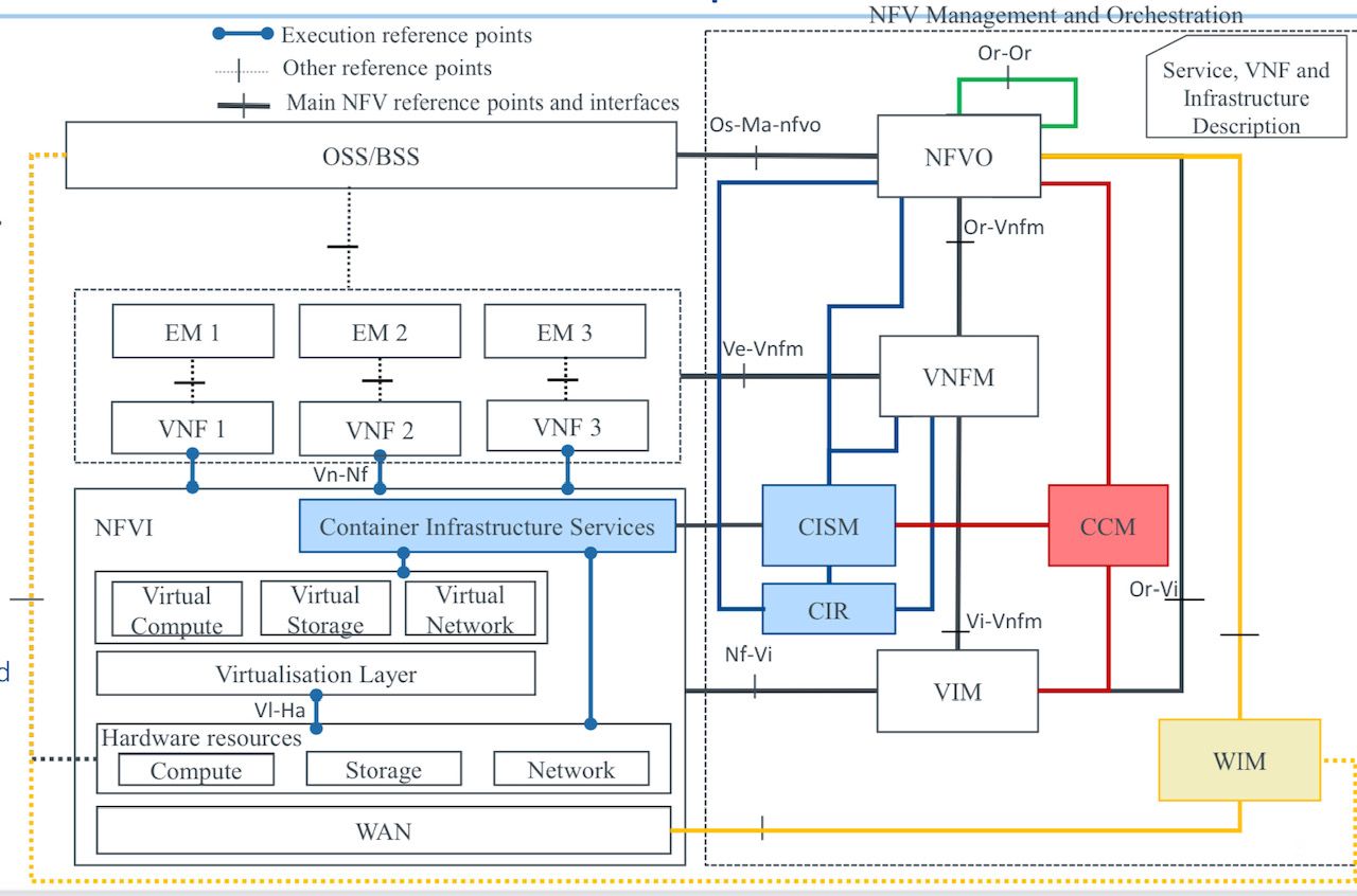


 Deutsche Telekom’s ongoing ORAN trial in Berlin uses key components from the ONF including the SD-Fabric, 5G and 4G core functions, and the uONOS near real-time RAN Intelligent controller (RIC). Source: ONF, DT.