
A career in technology market analysis
John Lively reflects on a 30-year career.
It was a typical workday in 1989, sitting through a meeting announcing the restructuring of Corning’s planar coupler business.
The speaker’s final words were, “Lively, you’ll be doing forecasting.” It changed my life and set my career path for the next 30-plus years.
No one grows up with a desire to be a market analyst. Indeed, I didn’t ask for the job. What made it possible was an IBM PC and LOTUS 1-2-3 in my marine biology lab in the early 1980s (a story for another time).
After a stop at MIT for an MBA, this led to a job in Corning’s fledgling PC support team in 1985. Then it was Corning’s optical fibre business cost-modelling fibre-to-the-home networks on a PC, working with Bellcore and General Instrument engineers. From there, it was to forecast market demand for planar couplers in the FTTH market.
In the following decade, I had various market forecasting roles within Corning’s optical fibre and photonics businesses.
Each time I tried to put forecasting behind me by taking a marketing or product management job, management said they needed me to return to forecasting due to some crisis or another (thank you, Bernie Ebbers).
In 1999, I had an epiphany. If Corning thinks I’m better at forecasting than anything else, perhaps I should become a professional forecaster in a company whose product is forecasts.
Just then, through fate or coincidence, I received a call from fellow MIT alum Dana Cooperson who said her firm, RHK, was desperate for people and did I know anyone who might be interested?
For the uninitiated, that’s code for ‘would you be interested in joining us?’.
I joined just in time to enjoy the remaining months of the boom, followed by a bust in 2001. But all the while learning to be a market analyst in a new context. While at Corning, I had been both a producer and procurer of market research. At RHK, I was strictly a producer.
More importantly, there was a direct link between my words and spreadsheets and money coming in. It was exhilarating.
Working remotely
Thanks to the newly deployed cable modem/ HFC technology that I had been cost-modelling a decade earlier, I was working from home.
I have worked from home ever since, and I can say that remote working does work well for some people and jobs.
Some lessons I’ve learned include:
- Working from home works best if the entire firm, not just a few people, are doing it.
- Home working doesn’t mean you can’t travel, pandemics notwithstanding.
- Home workers need to have clear deliverables that they can be judged against. Give them responsibility for something tangible, with an unambiguous deadline.
- Requiring time-tracking sheets or online monitoring of home workers is insulting and demotivating.
- Companies must support home workers by investing in quality internet services and conferencing software/ equipment on both sides of the link
Required skills
By joining RHK, I had moved from a Fortune 500 company to one of 100 employees. Over the next two decades, I would move between large and small companies. I prefer small companies because it’s clear who contributes to their success and who doesn’t. Poor performers have nowhere to hide in a company of six people.
After more than 30 years in the market research arena, I have views on the role of a market analyst and the talents necessary to be a good one.
The goal of market analysis is to find information, analyse it, draw conclusions, then package and communicate it.
Doing market research is like assembling a jigsaw puzzle, from which several pieces are missing. Or, like a chef who must create a healthy, enjoyable meal from an assortment of good and bad raw ingredients.
A technology market analyst should be intellectually curious, have a solid background in sciences and technology, and have broad industry knowledge, i.e., understand the jargon, the tech, and the companies.
The analyst also needs to write concisely and quickly, is fluent in Excel, PowerPoint, and Word, is a great communicator and is approachable, likeable, and outgoing.
Of course, finding all the requisite skills in one person is rare, and larger companies commonly divide duties into specialities like data collection, analysis, and communication.
In small companies, this may not be overt but happens to a degree just the same.
Most importantly, a market analyst must be comfortable with uncertainty.
One never has all the pieces, and you must be OK filling in missing data points via extrapolation, intuition, historical parallels, or other means. And be comfortable admitting your mistakes and adjusting your findings when new data surfaces.
I believe this is why those with a scientific background are better suited to market research than engineers. Scientists are taught scepticism and revision as a way of life, while engineers seek the certainty of the ‘right’ answer.
Periods of note
Throughout my career, I’ve lived through interesting times.
Starting in 1985, it was the introduction of the first PCs into Corning and establishing their first email system, electronic newsletter, word processing, and expert-learning systems.
Then, in the mid-1990s working in the early days of amplified DWDM systems and when the EDFA business doubled its output yearly.
Then came the Internet bubble and optical industry boom/bust of 1999-2001, when dozens of companies were founded by a couple of PhDs with a PowerPoint presentation. At one point in 2000, my optical components practice at RHK had over 100 subscribing companies.
It was weird living through an episode that we knew would someday be written about, like the Dutch tulip mania of 1634.
More recently, and I believe, with a more positive outcome, it is/ has been fascinating to watch companies like Alphabet, Amazon, and Meta utilise a globally connected internet to become the first truly global communications, media, and retail companies.
Moreover, these companies transcend national, cultural, and language boundaries, connecting a billion or more users. And in the process, inventing hyperscale data centres, which in turn allow hundreds and thousands of other companies to ‘cloudify’ as well, extending their global reach.
Of all the innovations and changes taking place today, this is one I will continue to follow with wonder and amazement.
The promise of these companies is so great that I’m hopeful they will become beacons of positive change around the world in the 21st century.
Innovation has been breathtaking in optics. For example, coherent transport, the far-out science stuff of technical talks at my first OFC in 1988, is in commercial use.
We blithely speak of optical transceivers capable of Terabit-per-second speeds without stopping to think how amazing it is that anything, anywhere, could be made to turn off and on again, one TRILLION times a second!
It simply defies human understanding, and yet we make it easy.
A view of now
Today, it’s easy to be convinced that things are falling apart, between Russia’s war against Ukraine, COVID, economic turmoil, screwed-up supply chains, and populist politicians.
But I take solace that I’ve seen things like this before and lived through them. As a child, scenes of the Vietnam war were on the news every evening. But finally, there was peace in Vietnam.
In the 1970s, we had an oil embargo and sky-high gas prices. It also ended.
In the 1980s, inflation ran hot, pushing my student loan interest rate to 13%. But I paid it off, and rates came down.
AIDS struck fear and stoked prejudice for years, claiming my aunt and uncle before scientists uncovered its secrets and developed effective treatments.
So it will be with COVID. History shows that humans tire of strife and disease and will work to conquer our worst problems eventually.
Surprises
Two things come to mind regarding industry surprises over the last 30 years.
One is that optical technology keeps advancing. Despite how challenging each new generation seems, bit by bit and idea by idea, the industry collectively comes up with a solution, and the subsequent speed hike is commercialised.
Another is how people find ways to use it no matter how much bandwidth is created. RHK founder, John Ryan, was fond of telling us, “Bandwidth is like cupboard space; it’s never left empty for long.”
Another surprising thing is how long the interpersonal bonds formed at RHK have lasted.
Though it was just a flash in time, many of those who were there in 2000 remain connected as friends and colleagues more than 20 years later.
Several such alumni work at LightCounting now.
Climate Change
While doing all this, looking backwards and reflecting on change, I couldn’t help dwelling on another major problem we face today: climate change.
Forestalling climate change is the one thing I believe where humans are failing. But unfortunately, the causes are so rooted in our global socio-economic systems that citizens and governments are not capable of inflicting the necessary sacrifices on themselves.
I fear the worst-case scenarios are coming soon, with shifting temperature zones and rising seas. In response, many people, plants, and animals will migrate, following favourable conditions north or south or inland as the case may be, significantly increasing competition for resources of all kinds.
I also fear authoritarian governments may prove more effective at providing protection for some, and avoiding utter chaos, than our precious but fragile democracies.
A role for tech giants
I think the internet and companies with global reach can play a role in combatting the worst impacts of climate change.
Some of the hyperscalers, telecom operators, and equipment companies have been leaders in reducing carbon emissions.
I hope the interconnectedness and massive computing power of companies like Meta and Alphabet can be used to solve these large-scale problems.
My last thought is the realisation that when I eventually ease into retirement and cut back on travel, I may never get a chance to personally thank all the friends and colleagues I have made along the way.
People who have assisted my career, believed in me, educated me, and made me think differently, smile, and laugh.
So, just in case, I’ll say it here – thank you one and all – you made a difference to me.
It’s also been fun.

Broadcom samples the first 51.2-terabit switch chip

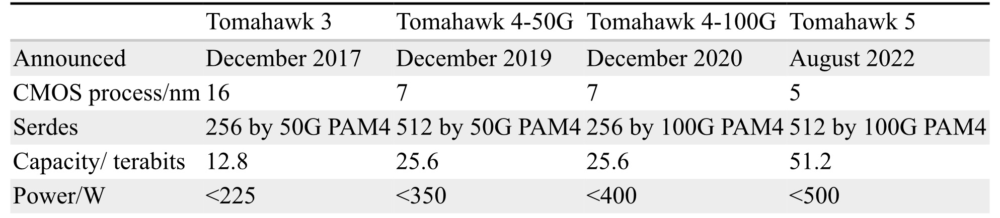
- Broadcom’s Tomahawk 5 marks the era of the 51.2-terabit switch chip
- The 5nm CMOS device consumes less than 500W
- The Tomahawk 5 uses 512, 100-gigabit PAM-4 (4-level pulse amplitude modulation) serdes (serialisers-deserialisers)
- Broadcom will offer a co-packaged version combining the chip with eight 6.4 terabit-per-second (Tbps) optical engines
Part 1: Broadcom’s Tomahawk 5
Broadcom is sampling the world’s first 51.2-terabit switch chip.
With the Tomahawk 5, Broadcom continues to double switch silicon capacity every 24 months; Broadcom launched the first 3.2-terabit Tomahawk was launched in September 2014.
“Broadcom is once again first to market at 51.2Tbps,” says Bob Wheeler, principal analyst at Wheeler’s Network. “It continues to execute, while competitors have struggled to deliver multiple generations in a timely manner.”
Tomahawk family
Hyperscalers use the Tomahawk switch chip family in their data centres.
Broadcom launched the 25.6-terabit Tomahawk 4 in December 2019. The chip uses 512 serdes, but these are 50-gigabit PAM-4. At the time, 50-gigabit PAM-4 matched the optical modules’ 8-channel input-output (I/O).
Certain hyperscalers wanted to wait for 400-gigabit optical modules using four 100-gigabit PAM-4 electrical channels, so, in late 2020, Broadcom launched the Tomahawk4-100G switch chip, which employs 256, 100-gigabit PAM-4 serdes.
Tomahawk 5 doubles the 100-gigabit PAM-4 serdes to 512. However, given that 200-gigabit electrical interfaces are several years off, Broadcom is unlikely to launch a second-generation Tomahawk 5 with 256, 200-gigabit PAM-4 serdes.
Switch ICs
Broadcom has three switch chip families: Trident, Jericho and the Tomahawk.
The three switch chip families are needed since no one switch chip architecture can meet all the markets’ requirements.
With its programable pipeline, Trident targets enterprises, while Jericho targets service providers.
According to Peter Del Vecchio, Broadcom’s product manager for the Tomahawk and Trident lines, there is some crossover. For example, certain hyperscalers favour the Trident’s programmable pipeline for their top-of-rack switches, which interface to the higher-capacity Tomahawk switches chips at the aggregation layer.
Monolithic design
The Tomahawk 5 continues Broadcom’s approach of using a monolithic die design.
“It [the Tomahawk5] is not reticule-limited, and going to [the smaller] 5nm [CMOS process] helps,” says Del Vecchio.
The alternative approach – a die and chiplets – adds overall latency and consumes more power, given the die and chiplets must be interfaced. Power consumption and signal delay also rise whether a high-speed serial or a slower, wider parallel bus is used to interface the two.
Equally, such a disaggregated design requires an interposer on which the two die types sit, adding cost.
Chip features
Broadcom says the capacity of its switch chips has increased 80x in the last 12 years; in 2010, Broadcom launched the 640-gigabit Trident.
Broadcom has also improved energy efficiency by 20x during the same period.
“Delivering less than 1W per 100Gbps is pretty astounding given the diminishing benefits of moving from a 7nm to a 5nm process technology,” says Wheeler.
“In general, we have achieved a 30 per cent plus power savings between Tomahawk generations in terms of Watts-per-gigabit,” says Del Vecchio.

These power savings are not just from advances in CMOS process technology but also architectural improvements, custom physical IP designed for switch silicon and physical design expertise.
“We create six to eight switch chips every year, so we’ve gotten very good at optimising for power,” says Del Vecchio
The latest switch IC also adds features to support artificial intelligence (AI)/ machine learning, an increasingly important hyperscaler workload.
AI/ machine learning traffic flows have a small number of massive ‘elephant’ flows alongside ‘mice’ flows. The switch chip adds elephant flow load balancing to tackle congestion that can arise when the two flow classes mix.
“The problem with AI workloads is that the flows are relatively static so that traditional hash-based load balancing will send them over the same links,” says Wheeler. “Broadcom has added dynamic balancing that accounts for link utilisation to distribute better these elephant flows.”
The Tomahawk 5 also provides more telemetry information so data centre operators can better see and tackle overall traffic congestion.
The chip has added virtualisation support, including improved security of workloads in a massively shared infrastructure.
Del Vecchio says that with emerging 800-gigabit optical modules and 1.6 terabit ones on the horizon, the Tomahawk 5 is designed to handle multiples of 400 Gigabit Ethernet (GbE) and will support 800-gigabit optical modules.
The chip’s 100-gigabit physical layer interfaces are combined to form 800 gigabit (8 by 100 gigabit), which is fed to the MAC, packet processing pipeline and the Memory Management Unit to create a logical 800-gigabit port. “After the MAC, it’s one flow, not at 400 gigabits but now at 800 gigabits,” says Del Vecchio.
Market research firm, Dell’Oro, says that 400GbE accounts for 15 per cent of port revenues and that by 2026 it will rise to 57 per cent.
Broadcom also cites independent lab test data showing that its support for RDMA over Converged Ethernet (RoCE) matches the performance of Infiniband.
“We’re attempting to correct the misconception promoted by competition that Infiniband is needed to provide good performance for AI/ machine learning workloads,” says Del Vecchio. The tests used previous generation silicon, not the Tomahawk 5.
“We’re saying this now since machine learning workloads are becoming increasingly common in hyperscale data centres,” says Del Vecchio.
As for the chip’s serdes, they can drive 4m of direct attached copper cabling, with sufficient reach to connect equipment within a rack or between two adjacent racks.
Software support
Broadcom offers a software development kit (SDK) to create applications. The same SDK is common to all three of its switch chip families.
Broadcom also supports the Switch Abstraction Interface (SAI). This standards-based programming interface sits on top of the SDK, allowing the programming of switches independent of the silicon provider.
Broadcom says some customers prefer to use its custom SDK. It can take time for changes to filter up, and a customer may want something undertaken that Broadcom can develop quickly using its SDK.
System benefits
Doubling the switch chip’s capacity every 24 months delivers system benefits.That is because implementing a 51.2-terabit switch using the current generation Tomahawk 4 requires six such devices.

Now a single 2-rack-unit (2RU) Tomahawk 5 switch chip can support 64 by 800-gigabit, 128 by 400-gigabit and 256 by 200-gigabit modules.
These switch boxes are air-cooled, says Broadcom.
Co-packaged optics
In early 2021 at a J.P Morgan analyst event, Broadcom revealed its co-packaged optics roadmap that highlighted Humboldt, a 25.6-terabit switch chip co-packaged with optics, and Bailly, a 51.2-terabit fully co-packaged optics design.
At OFC 2022, Broadcom demonstrated a 25.6Tbps switch that sent half of the traffic using optical engines.
Also shown was a mock-up of Bailly, a 51.2 terabit switch chip co-packaged with eight optical engines, each at 6.4Tbps.
Broadcom will offer customers a fully co-packaged optics Tomahawk 5 design but has not yet given a date.
Broadcom can also support a customer if they want tailored connectivity with, say, 3/4 of the Tomahawk 5 interfaces using optical engines and the remainder using electrical interfaces to front panel optics.
ADCs key for high baud-rate coherent systems

Increasing the baud rate of coherent modems benefits optical transport. The higher the baud rate the more data can be sent on a wavelength, reducing the cost-per-bit of traffic.
But engineers have become so good at designing coherent systems that they are now approaching the Shannon limit.
At the OFC show earlier this year, Ciena showcased a coherent module operating at 107 gigabaud (GBd). And last year, Acacia, now part of Cisco, announced its next-generation 1.2 terabits-per-second (Tbps) wavelength coherent module operating at up to 140GBd.
The industry believes that increasing the baud rate to 240+GBd is possible, but each new symbol-rate hike is challenging.
All the components in a modem – the coherent DSP and its digital-to-analogue (DAC) and analogue-to-digital (ADC) converters, the optics, and the analogue drive circuitry – must scale in lockstep.
Gigabaud and giga-samples
Coherent DSPs continue to improve in optical performance with each new CMOS process. The latest DSPs will use 5nm CMOS, while the semiconductor industry is developing 3nm CMOS and beyond.
Optical device performance is also scaling. For example, a 220GBd thin-film lithium niobate modulator has been demonstrated in the lab, while photodetectors will also achieve similar rates.
However, the biggest challenge facing coherent modem engineers is the analogue drive circuitry and the coherent DSP’s ADCs and DACs.
A key performance metric is its sampling rate measured in giga-samples-per-second (Gsps).

According to Nyquist, a signal needs to be sampled at twice its baud rate to be perfectly reconstructed. But that doesn’t mean sampling is always done at twice the baud rate. Instead, depending on the DSP implementation, the sampling rate is typically 1.2-1.6x the symbol rate.
“So, for a 200 gigabaud coherent modem, the DSP’s converters must operate at 240+ giga-samples per second,” says Tomislav Drenski, marketing manager, wireline, at Socionext Europe.
Socionext
Socionext is a system-on-chip specialist founded in 2015 with the combination of the system LSI divisions of Fujitsu and Panasonic, with its headquarters in Japan. Its European arm focuses on mixed-signal design, especially ADC, DACs and serialisers/ deserialisers (Serdes).
The company has developed 8-bit converters for several generations of long-haul optical designs, at 200Gbps, 400Gbps and greater than 1Tbps (see bottom photo). These optical systems used ADCs and DACs operating at 65, 92 and 128Gsps, respectively.
Socionext works with leading coherent optical module and network system providers but is also providing 5G and wireless ASIC solutions.
“We design the ADCs and DACs, which are ultra-high-speed, state-of-the-art circuit blocks, while our partners have their ideas on how the DSP should look,” says Drenski. “They provide us the DSP block, and we integrate everything into one chip.”
It is not just the quality of the circuit block that matters but how the design is packaged, says Drenski: “If the crosstalk or the losses in the package are too high, then whatever you have got with the IP is lost in the packaging.”
Any package-induced loss or added capacitance decreases bandwidth. And bandwidth, like sampling rate, is key to achieving high baud-rate coherent systems.
Design considerations
An important ADC metric is its resolution: the number of bits it uses to sample a signal. For high-performance coherent designs, 8-bit ADCs are used. However, because of the high sampling rate required and the associated jitter performance, the effective number of bits (ENOB) – an ADC metric – reduces to some 6 bits.
“People are asking for 10-bit converters for newer generations of design; these are shorter reach, not ultra-long-haul,” says Drenski.
Extra bits add fidelity and enable the recovery of higher-order modulated signals. Still, for ultra-long-haul, where the optical loss is more significant, using a 10-bit ADC makes little sense.
For 5G and wireless applications, higher resolutions, even going up to 14bit, is the recent trend. But such solutions use a lower sampling rate – 30Gsps – to enable the latest, direct-RF applications.

ADC architecture
An interleaved architecture enables an 8-bit ADC to sample a signal 128 billion times a second.
At the input to the ADC sits a sample-and-hold circuit. This circuit feeds a hierarchy of interleaved ‘sub-ADCs’. The interleaving goes from 1 to 4, then 4 to 16, 16 to 64, with the sub-ADCs all multiplexed.
“You take the signal and sample-and-hold it, then push everything down to many sub-ADCs to have the necessary speed at the end, at the output,” says Drenski.
These sub-ADCs must be aligned, and that requires calibration.
An ADC has three key metrics: sampling rate, bandwidth and ENOB. All three are interdependent.
For example, if you have a higher bandwidth, you will have a higher frequency, and clock jitter becomes a limiting factor for ENOB. Therefore, the number of sub-ADCs used must be well balanced and optimised to realise the high sampling frequencies needed without affecting ENOB. The challenge for the designer is keeping the gain, bias and timing variations to a minimum.
Drenski says designing the ADC is more challenging than the DAC, but both share common challenges such as clock jitter and also matching the path lengths of the sub-DACs.
240 gigabaud coherent systems
Can the bandwidth of the ADC reach 240+GBd?
“It all comes down to how much power you can spend,” says Drenski. “The more power you can spend to linearise, equalise, or optimise, the better.”
Noise is another factor. The amount of noise allowed determines how far the bandwidth can be increased. And with higher bandwidth, there is a need for higher clock speeds. “If we have higher clock speeds, we have higher complexity, so everything gets more complicated,” says Drenski.
The challenges don’t stop there.
Higher sampling rates mean the number of sub-ADCs must be increased, affecting circuit size and power consumption. And limiting the power consumption of the coherent DSP is a constant challenge.
At some point, the physical limitations of the process – the parasitics – limit bandwidth, independent of how the ADC circuitry is designed.
Coherent optics specialists like Acacia, Nokia, ADVA and Lumentum say that 220-240 gigabaud coherent systems are possible and will be achieved before the decade’s end.
Drenski agrees but stresses just how challenging this will be.
For him, such high baud rate coherent systems will only be possible if the electronics and optics are tightly co-integrated. Upping the bandwidth of each essential element of the coherent system, like the coherent DSP’s ADCs and DACs, is necessary but will not work alone.
What is needed is bringing both worlds together, the electronics and the optics.

Europe's first glimpse of a live US baseball game

It is rare to visit a museum dedicated to telecoms, never mind one set in beautiful grounds. Nor does it often happen that the visit coincides with an important anniversary for the site.
La Cité des Télécoms, a museum set in 11 hectares of land in Pleumeur-Bodou, Brittany, France, is where the first TV live feed was sent by satellite from the US to Europe.
The Telstar 1 communications satellite was launched 60 years ago, on July 10, 1962. The first transmission that included part of a live Chicago baseball game almost immediately followed.
By then, a vast horn radio antenna had been constructed and was awaiting the satellite’s first signals. The Radôme houses the antenna, an inflated dome-shaped skin to protect it from the weather. The antenna is built using 276 tonnes of steel and sits on 4,000 m3 of concrete. Just the bolts holding together the structure weigh 10 tonnes. It is also the largest inflated unsupported dome in the world.
The antenna continued to receive satellite transmissions till 1985. The location was then classed as a site of national historical importance. The huge horn antenna is unique since the twin antenna in the US has been dismantled.
The Cité des Télécoms museum was opened in 1991 and the site is a corporate foundation supported by Orange.
History of telecoms
A visitor to the museum is guided through a history of telecoms.
The tour begins with key figures of telecom such as Samuel Morse, Guglielmo Marconi, Lee de Forest and Thomas Edison. Lesser known inventors are also included, like Claude Chappe, who developed a semaphore system that eventually covered all of France.
The tour moves on to the advent of long-distance transmission of messages using telegraphy. Here, a variety of exquisitely polished wooden telegraphy systems are exhibited. Also included are rooms that explain the development of undersea cables and the advent of optical fibre.

In the optical section, an exhibit allows a user to point a laser at different angles to show how internal reflection of an optical fibre always guides the incident light to the receiver.
Four video displays expertly explain to the general public what is single-mode fibre, optical amplification, wavelength-division multiplexing, forward error correction, and digital signal processing.
The digital age
Radio waves and mobile communications follow before the digital world is introduced, starting with George Boole and an interactive display covering Boolean algebra. Other luminaries introduced include Norbert Wiener and Claude Shannon.
There are also an impressive collection of iconic computing and communications devices, including an IBM PC, the Apple II, an early MacBook, generations of mobile phones, and the French’s effort to computerise the country, the Minitel system, which was launced in 1982 and was only closed down in 2012.
The tour ends with interactive exhibits and displays covering the Web, Bitcoin and 5G.
The Radôme
The visit’s highlight is the Radôme.
On entering, you arrive in a recreated office containing 1960s engineering paraphernalia – a technical drawing board, slide rules, fountain pens, and handwritten documents. A guy (in a video) looks up and explains what is happening in the lead-up to the first transmission.

You then enter the antenna control centre and feel the tension and uncertainty as to whether the antenna will successfully receive the Telstra transmission. From there, you enter the vast dome housing the antenna.
TV displays take you through the countdown to the first successful transmission. Then a video display projected onto the vast ceiling gives a whistle-stop tour of the progress made since 1962: images sent from the moon landing in 1969, live World Cup football matches in 1970 through to telecom developments of the 1980s, 1990s, and 2000s.
The video ends with a glimpse of how telecoms may look in future.
Future of telecoms
The Radôme video is the closest the Cité des Télécoms museum comes to predicting the future and more would have been welcome.
But perhaps this is wise since, when you exit the Radome, a display bordering a circular lawn shows each key year’s telecom highlight from 1987 to 2012.
In 1987, the first optical cable linked Corsica to mainland Europe. The following year the first transatlantic optical cable (TAT-8) was deployed, while Bell Labs demonstrated ADSL in 1989.
The circular lawn display continues. In 1992, SMS was first sent, followed by the GSM standard in 1993. France Telecom’s national network became digital in 1995. And so it goes, from the iPhone in 2007 to the launch of 4G in Marseille in 2012.
There the display stops. There is no mention of Google, data centres, AI and machine learning, network functions virtualization, open RAN or 6G.

A day out in Brittany
The Radôme and the colossal antenna are a must-see, while the museum does an excellent job of demystifying telecoms. The museum is located in the Pink Granite Coast, a prime tourist attraction in Brittany.
Perhaps the museum’s key takeaway is how quickly digitisation and the technologies it has spawned have changed our world.
What lies ahead is anyone’s guess.

Hyperscalers' needs drive a new class of coherent DSP

Coherent digital signal processors (DSPs) companies have supported two families of coherent chips for some time. That’s because no single coherent DSP can meet all the market’s requirements.
The coherent DSP used for highest-performance optical transmissions must include advanced coding techniques, forward error correction, and a high symbol rate to send as much data as possible on a single wavelength and maximise reach.
In contrast, a DSP for coherent pluggable modules needs to be power-efficient and compact to meet the optical module’s power envelope and size constraints; a 400ZR QSFP-DD and a CFP2-DCO 400ZR+ being examples.
According to Ciena, now there is a need for a third category of coherent DSP for 1.6 terabit-per-second (Tbps) and 3.2Tbps transmissions over short distances for next-generation switch routers.
Carrying data centre payloads
The need comes from the hyperscalers, as with most emerging coherent optical applications. The new coherent DSP design is needed since it is the only way to support multi-terabit data rates for this application, says Ciena.
“Data centre switch routers with new 51.2- and 102.4-terabit switch chipsets will need greater than 400 gigabit-per-wavelength connectivity,” said Helen Xenos, senior director, portfolio marketing at Ciena, during a talk at NGON & DCI World, held in Barcelona in June.
The coherent DSP will connect equipment within a data centre and between data centre buildings on campus. A 1-10km reach for the 1.6Tbps or 3.2Tbps wavelength transmissions is needed using an industry-standard pluggable such as a QSFP-DD or a OSFP pluggable form factor.
“It would have to be a specific, very low-cost design,” says Xenos.
Coherent evolution
Applications using coherent optical technology continue to grow.
Subsea, long-haul, metro, and 80-120km data centre interconnect are all well-known markets for coherent optics, said Xenos. Now, coherent is moving to the access network and for unamplified single-channel links.
“There is no one coherent optical design that will be cost-optimal across all of these applications,” said Xenos. “This is why multiple coherent optical modem designs are required.”
Xenos last presented at NGON & DCI World in pre-pandemic 2019. Then, the questions were whether 800-gigabit wavelengths would be needed and what optical performance 400-gigabit coherent pluggables would deliver.
Much has since changed. There has been a broad deployment of optical transport equipment using 800-gigabit wavelengths while the coherent pluggable market has gone from strength to strength.
For the high-end, up to 800 gigabits per wavelength, 7nm CMOS DSPs are used, operating at a symbol rate of 90-110 gigabaud (GBd).
For 400-gigabit coherent pluggables operating, the symbol rate is 60-70GBd, while the optics used is mainly silicon photonics.
800-gigabit market
Ciena started shipping 800-gigabit capable optical modules in April 2020.
Since then, the company has seen strong uptake, with hyperscalers leading the way.

Also, a broad deployment of colourless, flexible grid optical line systems has helped 800-gigabit technology adoption.
Xenos cited, among others, Altibox, which brings high capacity connectivity from Norway to key digital hubs in Europe.
“They turned up the longest 800-gigabit wavelength between Copenhagen and Amsterdam, and that was over 1,100 kilometres,” she said.
400-gigabit pluggables
Xenos points out that there has been a halving of the power-per-bit at 400Gbps.
 Source: Ciena.
In 2017, Ciena offered a 400-gigabit 60GBd modem design in a 5×7-inch package.
“Now we have a pluggable 400-gigabit QSFP-DD at 60GBd pluggable, so the same type of design, the same simple feature set required with a 400ZR,” said Xenos.
Optical performance is also being pushed to 70GBd in the QSFP-DD, with the module having a higher output power.
Near-term designs
Ciena says the next two to three generations of coherent DSPs will use 5nm and 3nm CMOS.
New promising materials for optical modulation are emerging, such as thin-film lithium niobite, and barium titanate, which is compatible with silicon photonics.
“[A] Higher baud [rate] will reduce cost-per-bit and get more capacity using a single wavelength,” says Xenos. “Also, there will be more intelligence and programmability as we move forward to enable more automated networks.”
She says a 160GBd symbol rate is needed to send 800 gigabits over long-distance spans.
The key for all the different modem designs is to develop something better while choosing the right technologies so that new products are available promptly.
“It’s essential to make the right technology choice that will give the right reliability and be commercially available,” says Xenos.
Three nanometre CMOS promises more significant performance benefits for a DSP design, but developing the process technology is challenging for the leading chip fabrication plants. In addition, a 3nm CMOS process will be costly.
Award
Ciena won the optical vendor of the year award, one of the five prizes presented at the NGON & DCI World show.
Changing the radio access network for good

The industry initiative to open up the radio access network, known as open RAN, is changing how the mobile network is architected and is proving its detractors wrong.
So says a recent open RAN study by market research company, LightCounting.
“The virtual RAN and open RAN sceptics are wrong,” says Stéphane Téral, chief analyst at LightCounting.
Japan’s mobile operators, Rakuten Mobile and NTT Docomo, lead the world with large-scale open RAN deployments. Meanwhile, many leading communications service providers (CSPs) continue to trial the technology with substantial deployments planned around 2024-25.
Japan’s fourth and newest mobile network operator, Rakuten Mobile, deployed 40,000 open RAN sites with 200,000 radio units by the start of 2022.
Meanwhile, NTT Docomo, Japan’s largest mobile operator, deployed 10,000 sites in 2021 and will deploy another 10,000 this year.
NTT Docomo has shown that open RAN also benefits incumbent operators, not just new mobile entrants like Rakuten Mobile and Dish Networks in the US that can embrace the latest technologies as they roll out their networks.
Virtual RAN and open virtual RAN
Traditional RANs use a radio unit and a baseband unit from the same equipment supplier. Such RAN systems use proprietary interfaces between the units, with the vendor also providing a custom software stack, including management software.
The vendor may also offer a virtualised system that implements some or all of the baseband unit’s functions as software running on server CPUs.
A further step is disaggregating the baseband unit’s functions into a distributed unit (DU) and a centralised unit (CU). Placing the two units at different locations is then possible.
A disaggregated design may also be from a single vendor but the goal of open RAN is to enable CSPs to mix and match RAN components from different suppliers. Accordingly, the virtual RAN using open interfaces, as specified by the O-RAN Alliance, is an open virtual RAN system.
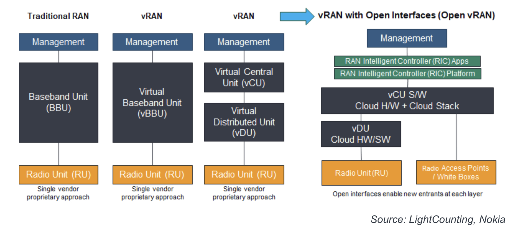
The diagram shows the different architectures leading to the disaggregated, virtualised RAN (vRAN) architecture.
Open virtual RAN comprises radio units, the DU and CU functions that can be implemented in the cloud, and the RAN Intelligent Controller (RIC), the brain of the RAN, which runs applications.
Several radio units may be connected to a virtual DU. The radio unit and virtual DU may be co-located or separate, linked using front-haul technology. Equally, the CU can host several virtual DUs depending on the networking requirements, connected with a mid-haul link.
Rakuten Mobile has deployed the world’s largest open virtual RAN architecture, while NTT Docomo has the world’s largest brownfield open RAN deployment.
NTT Docomo’s deployment is not virtualised and is not running RAN functions in software.
“NTT Docomo’s baseband unit is not disaggregated,” says Téral. “It’s a traditional RAN with a front-haul using the O-RAN Alliance specification for 5G.”
NTT Docomo is working to virtualise the baseband units and the work is likely to be completed in 2023.
Opening the RAN
NTT Docomo and the MGMN Alliance were working on interoperability between RAN vendors 15 years ago, says Téral. The Japanese mobile operator wanted to avoid vendor lock-in and increase its options.
“NTT Docomo was the only one doing it and, as such, could not enjoy economies of scale because there was no global implementation,” says Téral.
Wider industry backing arrived in 2016 with the formation of the Telecom Infra Project (TIP) backed by Meta (Facebook) and several CSPs to design network architectures that promoted interoperability using open equipment.
The O-RAN Alliance formed in 2018 was another critical development. With over 300 members, the O-RAN Alliance has ten working groups addressing such topics as defining the interfaces between RAN functions to standardise the open RAN architecture.
The O-RAN Alliance realised it needed to create more flexibility to enable boxes to be interchanged, says Téral, and started in the RAN to allow any radio unit to work with any virtual DU.
Geopolitics is the third element to kickstart open RAN. Removing Chinese equipment vendors Huawei and ZTE from key markets brought Open RAN to the forefront as a way to expand suppliers.
Indeed, Rakuten Mobile was about to select Huawei for its network, but it decided in 2018 to adopt open RAN instead because of geopolitics.
“Geopolitics added a new layer and, to some extent, accelerated the development of open RAN,” he says. “But it does not mean it has accelerated market uptake.”
That’s because the first wave of 5G deployments by the early adopter CSPs seeking a first-mover advantage is ending. Indeed, the uptake in 5G’s first three years has eclipsed the equivalent rollout of 4G, says LightCounting.
To date, over 200 of 800 mobile operators worldwide have deployed 5G.
Early 5G adopters have gone with traditional RAN suppliers like Ericsson, Nokia, Samsung, NEC and Fujitsu. And with open RAN only now hitting its stride, it has largely missed the initial 5G wave.
Open RAN’s next wave
For the next two years, then, the dominant open RAN deployments will continue to be those of Rakuten Mobile and NTT Docomo, to which can be added the network launches from Dish Networks in the US, and 1&1 Drillisch of Germany, which is outsourcing its buildout to Rakuten Symphony.
Rakuten Mobile’s vendor offshoot, Rakuten Symphony, set up to commercialise Rakuten’s open RAN experiences, is also working with Dish Networks on its deployment.
Rakuten Mobile hosts its own 5G network, including open RAN in its data centres. Dish is working with cloud player Amazon Web Services to host its 5G network. Dish’s network is still in its early stages, but the mobile operator can host its network in Amazon’s cloud because it uses a cloud-native implementation that includes Open RAN.
The next market wave for Open RAN will start in 2024-25 when the leading CSPs begin to turn off their 3G and start deploying Open RAN for 5G.
It will also be helped by the second wave of 5G rollouts those 600 operators with LTE networks. However, this second 5G cycle may not be as large as the first cycle, says Téral, and there will be a lag between the two cycles that will not be helped if there is a coming economic recession.
Specific leading CSPs that were early cheerleaders for open RAN has since dampened their deployment plans, says Téral. For example, Telefónica and Vodafone first spoke in 2019 of 1,000s of site deployments but have scaled back their deployment plans.
The leading CSPs explain their reluctance to deploy open RAN due to its many challenges. One is interoperability issues; despite the development of open interfaces, getting the different vendors’ components to work together is still a challenge.
Another issue is integration. Disaggregating the various RAN components means someone must stitch them together. Certain CSPs do this themselves, but there is a need for system integrators, and this is a challenge.
Téral believes that while these are valid concerns, Rakuten and NTT Docomo have already overcome such complications; open RAN is now deployed at scale.
These CSPs are also reluctant to end their relationships with established suppliers.
“The service providers’ teams have built relationships and are used to dealing with the same vendors for so long,” says Téral. “It’s very complicated for them to build new relationships with somebody else.”
More RAN player entrants
Rakuten Symphony has assembled a team with tremendous open RAN experience. AT&T is one prominant CSP that has selected Rakuten Symphony to help it with network planning and speed up deployments.
NTT Docomo working with four vendors, has got their radio units and baseband units to work with each other. In addition, NTT Docomo is also promoting its platform dubbed OREC (5G Open RAN Ecosystem) to other interested parties.
NEC and Fujitsu, selected by NTT Docomo, have also gained valuable open RAN experience. Fujitsu is a system integrator with Dish while NEC is involved in many open RAN networks in Europe, starting with Telefónica.
There is also a commercial advantage for these systems vendors since Rakuten Mobile and NTT Docomo are the leading operators, along with DISH and 1&1, deploying open RAN for the next two years.
That said, the radio unit business continues to look up. “There is no cycle [with radio units]; you still have to add radio units at some point in particular parts of the network,” says Téral.
But for open RAN, those vendors not used by NTT Docomo and Rakuten Mobile must wait for the next deployment wave. Vendor consolidation is thus inevitable; Parallel Wireless being the first shoe to drop with its recently announced wide-scale layoffs.
So while open RAN has expanded the number of vendor suppliers, further acquisitions should be expected, as well as companies folding that will not survive until the next deployment wave, says Téral.
And soon at the chip level too
There is also a supply issue with open RAN silicon.
With its CPUs and FlexRAN software, Intel dominates the open RAN market. However, the CSPs acknowledge there is no point in expanding RAN suppliers if there is a vendor lock-in at the chip level, one layer below.
Téral says several chip makers are working with system vendors to enter the market with alternative solutions. These include ARM-based architectures, AMD-Xilinx, Qualcomm, Marvell’s Octeon family and Nvidia’s BlueField-3 data processing unit.
The CSPs are also getting involved in promoting more chip choices. For example, Vodafone has set up a 50-strong research team at its new R&D centre in Malaga, Spain, to work with chip and software companies to develop the architecture of choice for Open RAN to expand the chip options.
Outlook
LightCounting forecasts that the open vRAN market will account for 13 per cent of the total global RAN sales in 2027, up from 4 per cent in 2022.
A key growth driver will be the global switch to open virtual RAN in 2024-25, driven by the large Tier 1 CSPs worldwide.
“Between 2025 and 2030, you will see a mix of open RAN, and where it makes sense in parts of the network, traditional RAN deployments too,” says Téral.

OpenLight's integrated-laser silicon photonics platform

- OpenLight is an independent silicon photonics company backed by Synopsys and Juniper Networks
- The company was created by carving out the silicon photonics arm of Juniper
- The establishment of OpenLight and its open platform highlights the growing maturity of silicon photonics as new applications emerge beyond datacom and telecom
OpenLight is coming to market with an open silicon photonics platform that includes integrated lasers and gain blocks.
Juniper has a long relationship with Synopsys, using its electronic-photonic design automation (EPDA) tools.
So when Juniper said it was spinning out its silicon photonics group, Synopsys was keen to partner. The result is OpenLight, of which Synopsys has a 75 per cent stake costing $67.5 million.
Thomas Mader, OpenLight’s chief operating officer and formerly head of Juniper’s silicon photonics unit, says OpenLight is the first company to offer an open platform that includes monolithically integrated lasers, optical amplifiers and modulators.
Juniper Networks and Synopsys
Juniper gained its silicon photonics technology in 2016 when it acquired Aurrion for $165 million.
Aurrion was a fabless silicon photonics start-up from the University of California, Santa Barbara, with a heterogeneous integration silicon photonics process that includes III-V materials, enabling integrated lasers as part of a photonic circuit.
OpenLight is now making this technology available through its partnership with the foundry Tower Semiconductor.
Juniper’s interests are mainly datacom and telecom, but it recognises the emerging opportunities for silicon photonics such as Lidar, optical computing, high-performance computing and optical interconnect.
“With this kind of technology, you want to drive volumes,” says Mader.

Juniper saw spinning out the unit and opening up access to the technology as the best way to drive volumes and reduce costs. The arrangement also benefits Juniper’s own technology needs.
Synopsys, meanwhile, believes it is the right time to back the OpenLight venture.
“We think it [the open platform] is a great opportunity for growth for Synopsys’s EPDA tools,” says John Koeter, senior vice president of marketing and strategy, solutions group at Synopsys.
OpenLight will give Synopsys insight into how the market is evolving and benefit the company’s tools and, eventually, its IP.
Business model
OpenLight is licensing its process design kit (PDK), the files that model Tower’s fabrication process. A company can enter into an agreement with Tower, access the PDK and design its silicon photonics device.
“What we are offering through Tower, and what we spent significant effort developing and showing Tower how to do, is monolithically integrating lasers and optical gain,” says Mader. “Tower is the first time we’re on a volume eight-inch [wafer] process.”
Juniper entered into a partnership with Tower Semiconductor in 2019.
“We are doing the first MPW [multi-project wafer] this summer with Tower on this process,” says Mader.
OpenLight is also providing designs it has developed and validated for several customers. “But we are not selling PICs [photonic integrated circuits]; that is not part of our plan,” says Mader.
OpenLight intends to partner with other foundries to make more widely available integrated-laser designs.

For now, though, OpenLight is focussed on ratifying its roadmap for the next two years.
“We’re going to be busy building out the component library for Tower to keep customers interested because better components make better circuits,” says Daniel Sparacin, vice president of business development and strategy at OpenLight.
OpenLight offers a 100-gigabit modulator and is working on its next-generation 200-gigabit modulator.
“We’re mostly O-band right now, and we have C-band coming up in the roadmap very shortly,” says Sparacin.
Applications
OpenLight has 400 and 800-gigabit optical designs for the data centre to help customers bring to market their PIC developments.
The company is also seeing interest from Lidar customers, particularly those pursuing coherent-based designs.
“The main reason is the integrated laser,” says Mader. “Otherwise, with standard silicon photonics, you have to attach a laser separately, which doesn’t scale well to multiple channels.” That’s because attaching multiple lasers impacts yield.
Lidar also benefits from on-chip optical amplification. “When you have a complex chip, you have a lot of losses,” says Mader.
OpenLight is working with firms pursuing optical computing for machine learning which promises greater power efficiency. “There are several of them coming to us because we can put hundreds or thousands of indium phosphide elements monolithically on a chip,” says Mader.
OpenLight says it has no position regarding co-packaged optics and whether a design uses an external light source or integrated lasers.
It believes co-packaged optics designs will eventually use integrated light sources, but its technology supports both and can even be used to make external light sources.
Overall, OpenLight says it is working with dozens of companies.
Design tools and integration
Synopsys has been an early mover with its integrated optical design automation tools. The tools include:
- OptoCompiler, a photonic IC design environment.
- The OptSim photonic circuit and system simulator.
- The Sentaurus TCAD and RSoft Photonic Device tools for process modelling and device design.
Working closely with OpenLight will benefit Synopsys’s tool environment, says Koeter. Synopsys is adding functionalities and design capabilities to its tools to support the integration of lasers. OpenLight is also providing Synopsys feedback on what will improve the experience of using its design platform.
Synopsys is one of three leading electronic design automation (EDA) tool companies. However, design tools for photonics are a more recent development.
“EDA quite a while ago is where photonic design is now going,” says Mader.
Integration is the underlying trend driving optics.
“We see the scaling already with 400- and 800-gigabit for datacom and some of the other applications; you see the shift to silicon photonics,” says Mader. “The higher the complexity, the more you see it shifting this way because there’s a cost advantage with the integrated laser and optical gain.”
Photonics may not come close to chip designs with billions of transistors. Still, photonic designs that go beyond four-channel design to ones with 32 or 64 channels or optical computing with hundreds or thousands of components are emerging.
“So you see a scaling even though it’s decades behind the electronics field,” says Mader.
With monolithically integrated lasers, yields remain high, whereas scaling a design with discrete components results in unacceptable yields.
“And so we will be able to go where you can’t go otherwise,” says Mader. “It’s not billions, but even dozens [of components] at this point is revolutionary.”
Intel adds multi-channel lasers to its silicon photonics toolbox
Intel has developed an 8-lane parallel-wavelength laser array to tackle the growing challenge of feeding data to integrated circuits (ICs).
Optical input-output (I/O) promises to solve the challenge of getting data into and out of high-end silicon devices.
These ICs include Ethernet switch chips and ‘XPUs’, shorthand for processors (CPUs), graphics processing units (GPUs) and data processor units (DPUs).
The laser array is Intel’s latest addition to its library of silicon photonics devices.
Power wall
A key challenge facing high-end chip design is the looming ‘power wall’. The electrical I/O power consumption of advanced ICs is rising faster than the power the chip consumes processing data.
James Jaussi, senior principal engineer and director, PHY research lab at Intel Labs, says if this trend continues, all the chip’s power will be used for communications and none will be left for processing, what is known as the power wall.
One way to arrest this trend is to use optical rather than electrical I/O by placing chiplets around the device to send and receive data optically.
Using optical I/O simplifies the electrical I/O needed since the chip only sends data a short distance to the adjacent chiplets. Once in the optical domain, the chiplet can send data at terabit-per-second (Tbps) speeds over tens of meters.
However, packaging optics with a chip is a significant design challenge and changes how computing and switching systems are designed and operated.

Laser array
Intel has been developing silicon photonics technology for two decades. The library of devices includes ring-resonators used for modulation and detection, photo-detectors, lasers, and semiconductor optical amplifiers.

Intel can integrate lasers and gain blocks given its manufacturing process allows for the bonding of III-V materials to a 300mm silicon wafer, what is known as heterogeneous integration.
The company has already shipped over 6 million silicon photonics-based optical modules – mainly its 100-gigabit PSM-4 and 100-gigabit CWDM-4 – since 2016.
Intel also ships such modules as the 100G LR4, 100G DR/FR, 200G FR4, 400G DR4 and 400G FR4. The company says it makes two million optical modules a year.
Now Intel Labs has demonstrated a laser array that integrates eight distributed feedback (DFB) lasers for wavelength-division multiplexing (WDM) transmissions. In addition, the laser array is compliant with the CW-WDM multi-source agreement.
“This is a much more difficult design,” says Haisheng Rong, senior principal engineer, photonics research at Intel Labs. “The challenge here is that you have a very small channel spacing of 200GHz.”
Each laser’s wavelength is defined by the structure of the silicon waveguide – less than 1 micron wide and tens of microns long – and the periodicity of a Bragg reflector grating.
The lasers in the array are almost identical, says Rong, their difference being defined by the Bragg grating’s period. There is a 0.2nm difference in the grating period of adjacent – 200GHz apart – lasers. For 100GHz spacing, the grating period difference will need to be 0.1nm.
Specifications
The resulting eight wavelengths have uniform separation. Intel says each wavelength is 200GHz apart with a tolerance of plus or minus 13GHz, while the lasers’ output power varies by plus or minus 0.25dB.
Such performance is well inside the CW-WDM MSA specifications that call for a plus or minus 50GHz tolerance for 200GHz channel spacings and plus or minus 1dB variability in output power.
Rong says that using a 200GHz channel enables a baud rate of 64 gigabaud (GBd) or 128GBd. Intel has already demonstrated its electronic and photonic ICs (EIC/ PIC) operating at 50 gigabit-per-second (Gbps) and 112Gbps.
In future, higher wavelength counts – 16- and 32-channel designs – will be possible, as specified by the CW-WDM MSA.
The laser array’s wavelengths vary with temperature and bias current. For example, the laser array operates at 80oC, but Intel says it can work at 100oC.
Products
The working laser array is the work of Intel Labs, not Intel’s Silicon Photonics Products Division. Intel has yet to say when the laser array will be adopted in products.
But Intel says the technology will enable terabit-per-second (Tbps) transmissions over fibre and reach tens of meters. The laser array also promises 4x greater I/O density and energy efficiency of 0.25 picojoules-per-bit (pJ/b), two-thirds that of the PCI Express 6.0 standard.
Another benefit of optical I/O is low latency, under 10ns plus the signal’s time of flight, determined by the speed of light in the fibre and the fibre’s length.
An electrical IC is needed alongside the optical chiplet to drive the optics and control the ring-resonator modulators and lasers. The chip uses a 28nm CMOS process and Intel is investigating using a 22nm process.
Optical I/O goals
Intel announced in December 2021 that it was working with seven universities as part of its Integrated Photonics Research Center.
The goal is to create building-block circuits that will meet optical I/O needs for the next decade-plus, says Jaussi.
Intel aims to demonstrate by 2024 sending 4Tbps over a fibre while consuming 0.25pJ/b.

Marvell plans for CXL's introduction in the data centre

The open interconnect Compute Express Link (CXL) standard promises to change how data centre computing is architected.
CXL enables the rearrangement of processors (CPUs), accelerator chips, and memory within computer servers to boost efficiency.
“CXL is such an important technology that is in high focus today by all the major cloud hyperscalers and system OEMs,” says Thad Omura, vice president of flash marketing at Marvell.
Semiconductor firm Marvell has strengthened its CXL expertise by acquiring Tanzanite Silicon Solutions.
Tanzanite was the first company to show two CPUs sharing common memory using a CXL 2.0 controller implemented using a field-programmable gate array (FPGA).
Marvell intends to use CXL across its portfolio of products.
Terms of the deal for the 40-staff Tanzanite acquisition have not been disclosed.
Data centre challenges
Memory chips are the biggest item spend in a data centre. Each server CPU has its own DRAM, the fast volatile memory overseen by a DRAM controller. When a CPU uses only part of the memory, the rest is inactive since other server processors can’t access it.
“That’s been a big issue in the industry; memory has consistently been tied to some sort of processor,” says Omura.
Maximising processing performance is another issue. Memory input-output (I/O) performance is not increasing as fast as processing performance. Memory bandwidth available to a core has thus diminished as core count per CPU has increased. “These more powerful CPU cores are being starved of memory bandwidth,” says Omura.
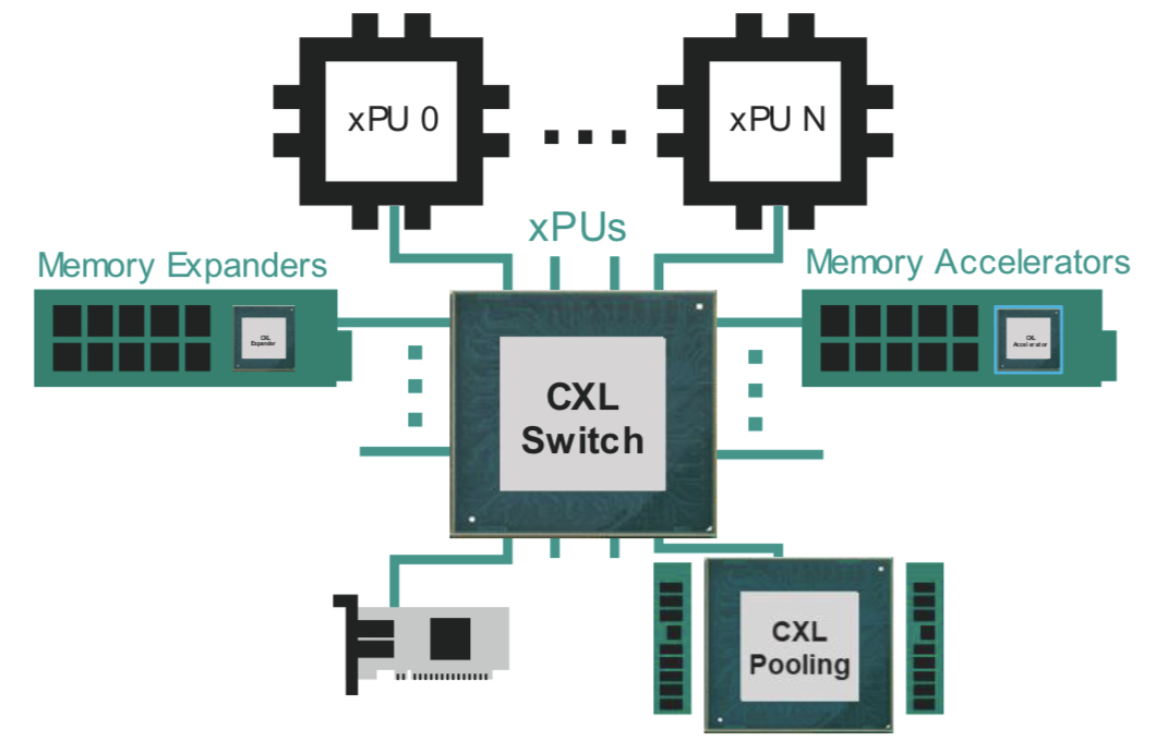
CXL tackles both issues: it enables memory to be pooled improving usage overall while new memory data paths are possible to feed the cores.
CXL also enables heterogeneous compute elements to share memory. For example, accelerator ICs such as graphic processing units (GPUs) working alongside the CPU on a workload.
CXL technology
CXL is an industry-standard protocol that uses the PCI Express (PCIe) bus as the physical layer. PCI Express is used widely in the data centre; PCIe 5.0 is coming to market, and the PCIe 6.0 standard, the first to use 4-level pulse-amplitude modulation (PAM-4), was completed earlier this year.
In contrast, other industry interface protocols such as OpenCAPI (open coherent accelerator processor interface) and CCIX (cache coherent interconnect for accelerators) use custom physical layers.
“The [PCIe] interface feeds are now fast enough to handle memory bandwidth and throughput, another reason why CXL makes sense today,” says Omura.
CXL supports low-latency memory transactions in the tens of nanoseconds. In comparison, the non-volatile memory express storage (NVMe), which uses a protocol stack run on a CPU, has tens of microseconds transaction times.
“The CXL protocol stack is designed to be lightweight,” says Omura. “It doesn’t need to go through the whole operating system stack to get a transaction out.”
CXL enables cache coherency, which is crucial since it ensures that the accelerator and the CPU see the same data in a multi-processing system.
Memory expansion
The first use of CXL will be to simplify the adding of memory.
A server must be opened when adding extra DRAM using a DIMM (dual in-line memory module). And there are only so many DIMM slots in a server.
The DIMM also has no mechanism to pass telemetry data such as its service and bit-error history. Cloud data centre operators use such data to oversee their infrastructure.
Using CXL, a memory expander module can be plugged into the front of the server via PCIe, avoiding having to open the server. System cooling is also more straightforward since the memory is far from the CPU. The memory expander’s CXL controller can also send telemetry data.
CXL also boosts memory bandwidth. When adding a DIMM to a CPU, the original and added DIMM share the same channel; capacity is doubled but not the interface bandwidth. Using CXL however opens a channel as the added memory uses the PCIe bus.
“If you’re using the by-16 ports on a PCIe generation five, it [the interface] exceeds the [DRAM] controller bandwidth,” says Omura.
Pooled memory
CXL also enables memory pooling. A CPU can take memory from the pool for a task, and when completed, it releases the memory so that another CPU can use it. Future memory upgrades are then added to the pool, not an individual CPU. “That allows you to scale memory independently of the processors,” says Omura.
The likely next development is for all the CPUs to access memory via a CXL switch. Each CPU will no longer needs a local DRAM controller but rather it can access a memory expander or the memory pool using the CXL fabric (see diagram above).
Going through a CXL switch adds latency to the memory accesses. Marvell says that the round trip time for a CPU to access its local memory is about 100ns, while going through the CXL switch to pooled memory is projected to take 140-160ns.
The switch can also connect a CXL accelerator. Here, an accelerator IC is added to memory which can be shared in a cache coherent manner with the CPU through the switch fabric (see diagram above).
I/O acceleration hardware can also be added using the CXL switch. Such hardware includes Ethernet, data processing unit (DPU) smart network interface controllers (smartNICs), and solid-state drive (SSD) controllers.
“Here, you are focused on accelerating protocol-level processing between the network device or between the CPU and storage,” says Omura. These I/O devices become composable using the CXL fabric.
More CXL, less Ethernet
Server boxes in the data are stacked. Each server comprises CPUs, memory, accelerators, network devices and storage. The servers talk to each other via Ethernet and other server racks using a top-of-rack switch.
But the server architecture will change as CXL takes hold in the data centre.

“As we add CXL into the infrastructure, for the first time, you’re going to start to see disaggregate memory,” says Omura. “You will be able to dynamically assign memory resources between servers.”
For some time yet, servers will have dedicated memory. Eventually, however, the architecture will become disaggregated with separate compute, memory and I/O racks. Moreover, the interconnect between the boxes will be through CXL. “Some of the same technology that has been used to transmit high-speed Ethernet will also be used for CXL,” says Omura.
Omura says deployment of the partially-disaggregated rack will start in 2024-25, while complete disaggregation will likely appear around the decade-end.
Co-packaged optics and CXL
Marvell says co-packaging optics will fit well with CXL.

“As you disaggregate memory from the CPU, there is a need to have electro-optics drive distance and bandwidth requirements going forward,” says Nigel Alvares, vice president of solutions marketing at Marvell.
However, CXL must be justified from a cost and latency standpoint, limiting its equipment-connecting span.
“The distance in which you can transmit data over optics versus latency and cost is all being worked out right now,” says Omura. The distance is determined by the transit time of light in fibre and the forward error correction scheme used.
But CXL needs to remain very low latency because memory transactions are being done over it, says Omura: “We’re no longer fighting over just microseconds or milliseconds of networking, now we’re fighting over nanoseconds.”
Marvell can address such needs with its acquisition of Inphi and its PAM-4 and optical expertise, the adoption of PAM-4 encoding for PCIe 6.0, and now the addition of CXL technology.

ADVA and II-VI’s coherent partnership

- ADVA and II-VI have jointly developed a 100-gigabit coherent DSP
- Both companies plan to use the 2.0-2.5W, 7nm CMOS Steelerton DSP for a 100ZR QSFP28 module
- II-VI’s ASIC design team engineered the DSP while ADVA developed the silicon photonics-based optics.
ADVA and II-VI have joined forces to define a tiny coherent digital signal processor (DSP) that fits inside a QSFP28 optical module.
The Steelerton DSP can send a 100-gigabit dense wavelength-division multiplexing (DWDM) transmission over 80-120km, carrying wireless backhaul and access traffic.
“It is backhaul of broadband, it is backhaul of mobile, and it definitely moves outdoors,” says Christoph Glingener, CTO at ADVA.
The module also serves metro networks with its 300km reach using optical amplification.
II-VI and ADVA now join such established coherent players as Ciena, Huawei, Infinera, Nokia as well as Marvell, NEL, and Acacia, now part of Cisco.
Effect Photonics announced at OFC earlier this year its coherent market entry with its acquisition of the Viasat DSP team.
Motivation
ADVA says it entered the coherent DSP market after failing to find a design suited for backhaul, a coherent market that promises highest unit volumes.
Backhaul has become even more important market for ADVA given its merger with broadband equipment maker ADTRAN.
II-VI also notes how access rates are moving from 10 to 100 gigabits.
“We were looking to develop a DSP capable to target a market that is underserved and where we can differentiate. This analysis led us to the 100ZR with a purpose-built DSP solution” says John DeMott, vice president product management, coherent and tunable product lines at II-VI.
The 100-gigabit coherent market for access contrasts with 400-gigabit coherent that uses modules such as 400ZR and 400ZR+ to connect data centres.
ADVA did consider existing suppliers’ coherent DSPs but deemed them too big and power-hungry for this application. This is what led to the II-VI partnership.
“We found a partner in II-VI that was willing to do this, but to get to the required power envelopes, we needed a 7nm DSP,” says Glingener. “And 7nm CMOS technology is not cheap.“
II-VI has a staff of mixed-signal and ASIC engineers in Germany that designed the Steelerton chip.
The two firms now have their own 100-gigabit DSP and can start developing coherent product roadmaps.
Applications
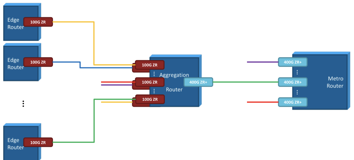
The 100ZR module will be deployed at aggregation sites.
ADVA shows how the 100ZR module is used for edge aggregation (see diagram).


Another application is 100-gigabit data-centre interconnect (DCI) for enterprises; hyperscalers require 400 gigabit and higher rates for DCI.
II-VI says the DSP is suited for access and metro applications. The 100ZR module fits a wavelength in a 50GHz channel to enable 96 DWDM wavelengths across the C-band. The 100ZR module has a maximum reach of 300km when used with amplification.
“The 22dB loss budget supports up to 80km without in-line amplification and up to 300km with in-line amplification, limited by chromatic dispersion,” says DeMott.
II-VI highlights several use-cases for the 100ZR module.
One is IP-over-DWDM, connecting edge routers to an aggregation router (see diagram) or a muxponder. The aggregated 100-gigabit wavelengths are sent to a metro router using a 400-gigabit 400ZR+ coherent module. II-VI also has 400ZR+ modules.
Two factors dictate the 100ZR module design: power consumption and the form factor.
Even a module power consumption of 10W is too high for access. Also, the DSP and optics must fit inside a QSFP28 since this is a common form factor for access equipment uplinks.
The resulting DSP has a power consumption of 2.0-2.5W and the chip is a fifth the size of other 7nm coherent DSPs. The 100ZR QSFP28 module – the DSP and optics – consumes 5.0-5.5W.
The DSP is stripped down to its essential features to achieve the power target. For example, the DSP uses one modulation format only: dual-polarisation, quadrature phase-shift keying (DP-QPSK).
“You de-feature the DSP down to a level that you can meet the power envelope, and it is not that complicated anymore,” says Glingener.
ADVA developed the silicon photonics analogue front end for the module that uses a single laser. To fit the DSP and the optics in a QSFP28 also proved an integration challenge.
The Steelerton DSP is taped out and both companies expect to have 100ZR prototype modules in the second half of this year.
What next
ADVA is planning a 100ZR+ module that will have enhanced optical performance that will be available in prototype form in early 2023.
ADVA’s coherent module interest remains broadband. Possible developments include a 5nm CMOS 200-gigabit DSP or a cheaper, more power-efficient, second-generation 100-gigabit design.
ADVA is also exploring concepts such as a parallel design, a 4x100G implementation.
Meanwhile, II-VI is looking at high-end coherent designs, which may include multiple sources for silicon photonics
“The next obvious steps are 800 gigabits and 1.6 terabits,” says DeMott. “There is a lot of [industry] activity, so those would be directions we’re considering.” II-VI has in-house optics for high-end coherent designs.
There will be a market for 800-gigabit coherent modules, says DeMott, but hyperscalers already are asking for 1.6-terabit designs.
“These are divergent DSPs,” says DeMott. “You can’t do a DSP that does 1.6 terabits, 800 gigabits and 400 gigabits; it’s either a 1.6-terabit or a 400/ 800-gigabit DSP design.”