Nokia jumps a class with its PSE-6s coherent modem
- The 130 gigabaud (GBd) PSE-6s coherent modem is Nokia’s first in-house design for high-end optical transport systems
- The PSE-6s can send an 800 gigabit Ethernet (800GbE) payload over 2,000km and 1.2 terabits of data over 100km.
- Two PSE-6s DSPs can send three 800GbE signals over two 1.2-terabit wavelengths
Nokia has unveiled its latest coherent modem, the super coherent Photonic Service Engine 6s (PSE-6s) that will power its optical transport platforms in the coming years.
The PSE-6s comes three years after Nokia announced its current generation of coherent digital signal processors (DSPs): the PSE-Vs DSP for the long-haul and the compact PSE-Vc for the coherent pluggable market.
Nokia is only detailing the PSE-6s; its next-generation coherent modem for pluggables will be a future announcement.
Nokia will demonstrate the PSE-6s at the upcoming OFC show in March while field trials involving systems using the PSE-6s will start in the year’s second half.
Reducing cost per bit
In 2020, Nokia bought Elenion, a silicon photonics company specialising in coherent optics.
The PSE-6s is Nokia’s first in-house coherent modem – the coherent DSP and associated optics – targeting the most demanding optical transport applications.
Nokia points out that coherent systems started approaching the Shannon limit two generations ago.
In the past, operators could reduce the cost of optical transport by sending more data down a fibre; upgrading the optical signal from 100 to 200 to 400 gigabit required only a 50GHz channel.
“You were getting more fibre capacity with each generation,” says Serge Melle, director of product marketing, optical networks at Nokia. And this helped the continual reduction of the cost-per-bit metric.
But with more advanced DSPs, implemented using 16nm, 7nm, and now 5nm CMOS, going to a higher symbol rate and hence data rate requires more spectrum, says Melle.
Increasing the symbol rate is still beneficial. It allows more data to be sent using the same modulation scheme or transmitting the same data payload over longer distances.
“So one of the things we are looking to do with the PSE-6s is how do we still enable a lower total cost of ownership even though you don’t get more capacity per wavelength or fibre,” says Melle.

Symbol rate classes
Coherent optics from the leading vendors use a symbol rate of 90-107 gigabaud (GBd), while Cisco-owned Acacia’s latest 1.2-terabit coherent modem in a CIM-8 module operates at 140GBd.
Acacia uses a classification system based on symbol rate. First-generation coherent systems operating at 30-34GBd are deemed Class 1. Class 2 doubles the baud rates to 60-68GBd, the symbol rate window used for 400ZR coherent optics, for hyperscalers to connect equipment across their data centres up to 120km apart.
The DSPs from the leading optical transport systems vendors operating at 90-107GBd are an intermediate step between Class 2 and Class 3 using Acacia’s classification. In contrast, Acacia has jumped directly from Class 2 to Class 3 with its 140GBd CIM-8 coherent modem.
Competitors view Acacia’s classification scheme as a marketing exercise and counter that their 90-107GBd optical transport systems benefited customers for over two years.
Nokia’s 90GBd PSE-Vs can send 400 gigabits using quadrature phase-shift keying (QPSK) over 3,000km. This contrasts with its earlier 67GBd PSE-3s that sends 400GbE up to 1,000km using 16-QAM.
However, with the PSE-Vs, Nokia, unlike its optical transport competitors, Infinera, Ciena and Huawei, decided not to support 800-gigabit wavelengths.
Nokia argued that 7nm CMOS, 90-100GBd coherent optics tops out at 600 gigabit when used for distances of several hundred kilometers, while metro-regional distances are more economically served using 400-gigabit pluggable optics such as the CFP2 implementing 400ZR+.
With the 130Gbd PSE-6s, Nokia has a Class 3 coherent modem with the PSE-6s capable of sending 800 gigabits more than 2,000km.
The PSE-6s also doubles the maximum data rate of the PSE-Vs to 1.2 terabits per wavelength. However, at 1.2 terabits, the reach is 100-plus km, valuable for very high capacity metro transport and data centre interconnect.
Scale, reach and power consumption per bit
Nokia highlights the PSE-6s’ main three performance metric improvements.
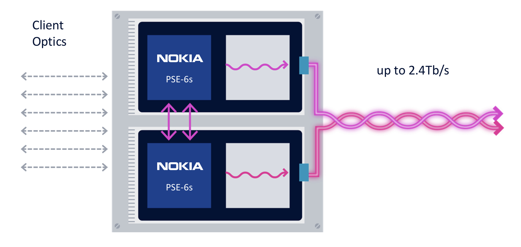
First, the coherent modem delivers scaling: two coherent optical engines fit on a line card to deliver 2.4 terabits to transport emerging high-speed services such as 800GbE.
The two PSE-6s are linked using a dedicated interface to share the client-side signals (see diagram).
“We are not the only ones introducing a 5nm solution, but I think we are the only ones that allow two DSPs to work together,” says Melle.
Without the interface, a single 800GbE and up to four 100GbE clients or a 400GbE client can be sent over each DSP’s 1.2-terabit wavelength. Adding the interface, an operator can send three uniform 800GbE clients, with the interface splitting the third 800GbE client between the two DSPs.
“In a single line card, you can stripe the three 800-gigabit services rather than have to deploy three separate line cards in the network,” says Melle.
Nokia is not detailing the interface used to link the DSPs but said that the interface is used for data only and not to share signal processing resources between the ASICs.
“There is an extra amount of circuitry to share the client bandwidth across the two DSPs, but it is not high power consuming, and most transponders have some circuitry between the clients and the DSP,” says Melle. “So the incremental ‘power tax’ is marginal; it doesn’t add any significant power overhead.”
The resulting 2.4-terabit transmission is sent as two 1.2-terabit wavelengths, each occupying a 150GHz-wide channel. Existing systems that operate at 90-107GBd typically use a 112.5GHz channel for an 800-gigabit transmission, so the PSE-6s delivers a fibre capacity benefit.
The two wavelengths can be bonded, as in a two-channel ‘super-channel’, or sent to separate locations.
The second improvement is optical performance. For example, an 800-gigabit payload can travel over 2,000km. Nokia claims this is 3x the reach of existing commercial optical transport systems.
The improved transmission performance is achieved using a combination of the 130GBd baud rate, probabilistic constellation shaping (PCS), and improved forward error correction (FEC). Melle says the contributions to the improvement are 90 per cent baud rate and 10 per cent due to coherent modem algorithm tweaks.
“Baud rate is king; that is what really drives this improved performance,” says Melle.
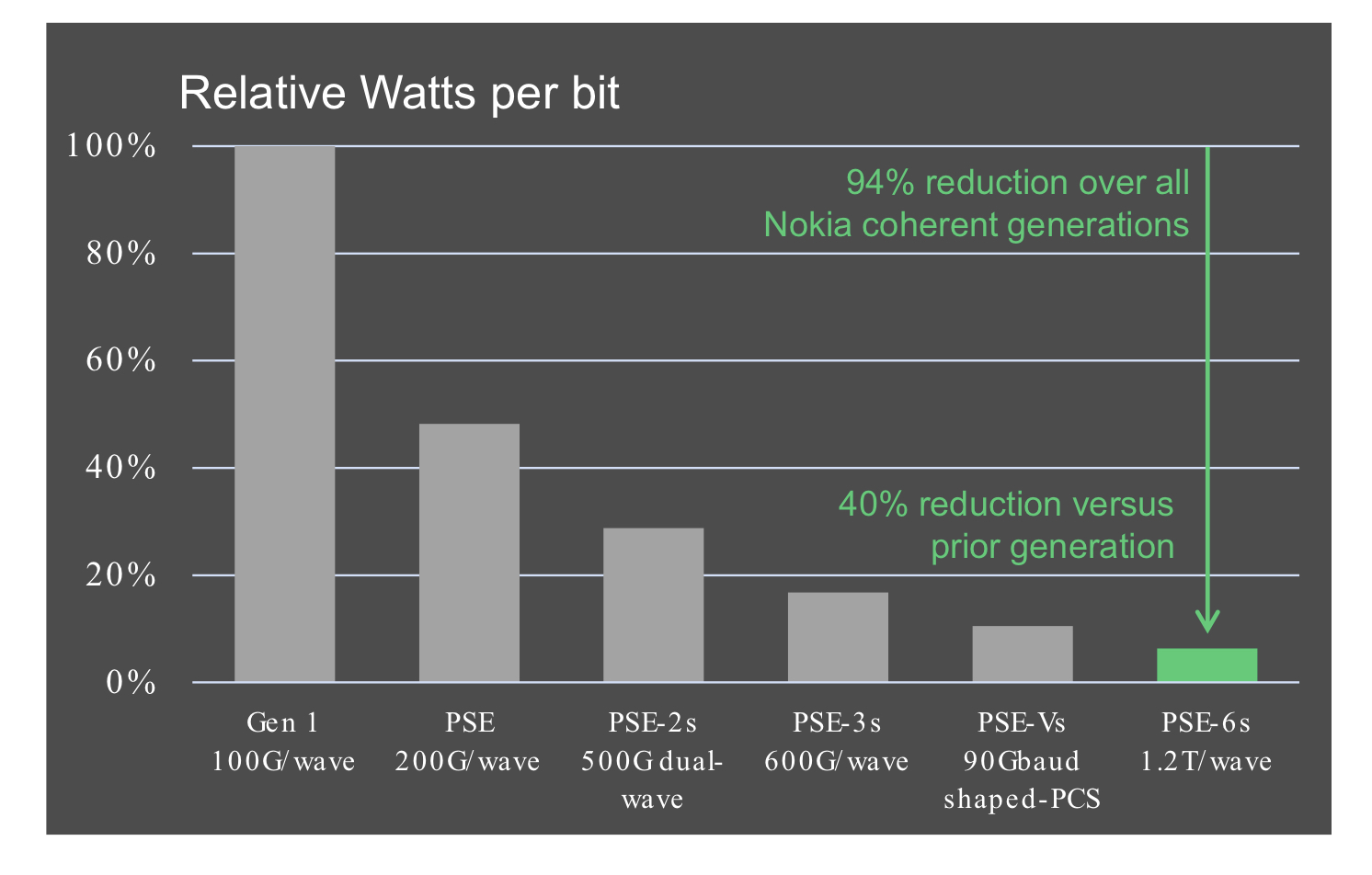
The third benefit is reduced power consumption at the device and system (networking) levels.
Using a 5nm finFET CMOS process to make the PSE-6s DSP ASIC and developing denser line cards (two modems per card) means systems will consume 60 per cent less power than Nokia’s existing coherent technology.
According to Nokia, the PSE-6s optical engine consumes 40 per cent fewer Watts per bit compared to the PSE-Vs.
Nokia 1830 transport systems
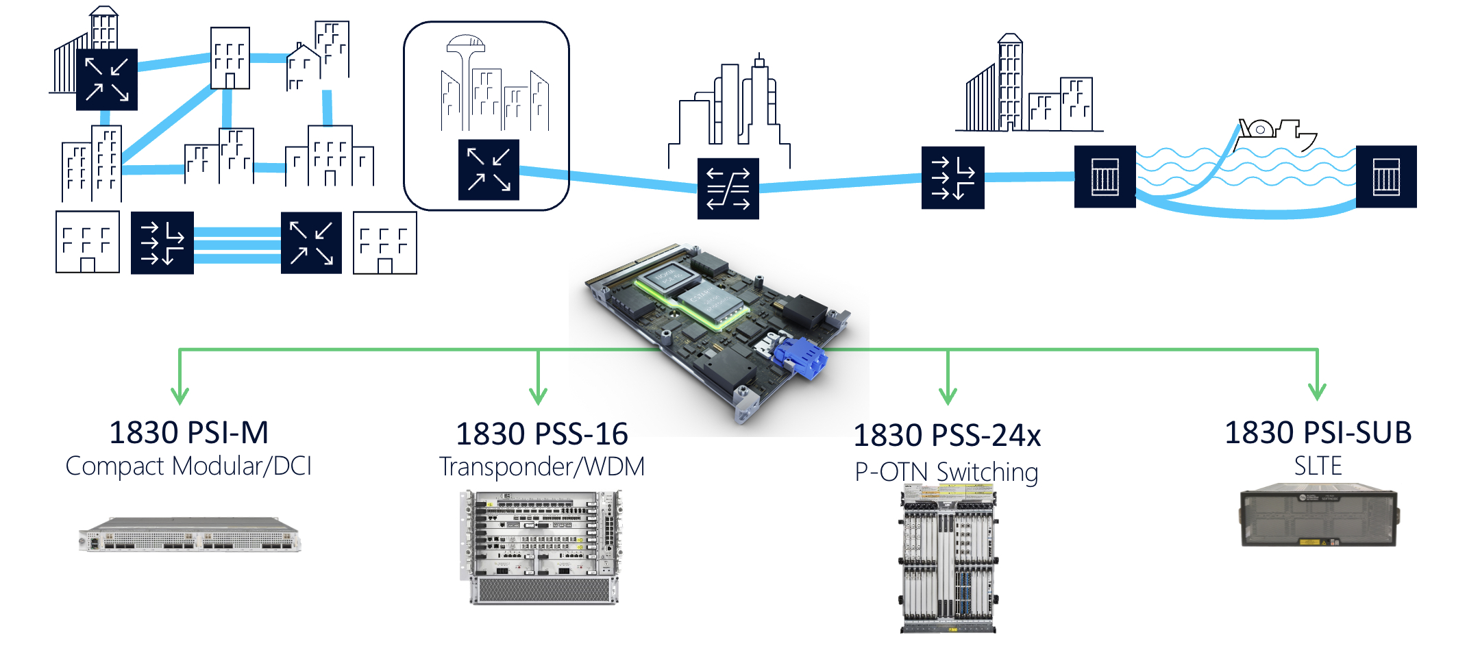
The PSE-6s line cards fit into Nokia’s existing range of 1830 transport platforms.
These include the 1830 PSI-M compact modular data centre interconnect, the 1830 PSS-16 transponder and WDM line system, the 1830 PSS-24x P-OTN and switching chassis, and the 1830 PSI-SUB subsea line-terminating equipment.
For example, the PSI-M platform can hold two line cards, each with two PSE-6s.
How to shepherd a company’s technologies for growth

CTO interviews part 3: Dr Julie Eng
- Eng is four months into her new role as CTO of Coherent.
- Previously, she headed Finisar’s transceiver business and then the 3D sensing business, first at Finisar and then at II-VI. II-VI changed its name to Coherent in September 2022
- “CTO is one of these roles that has no universal definition,” says Eng
ulie Eng loved her previous role.
She had been heading II-VI’s (now Coherent’s) 3D sensing unit after being VP of engineering at Finisar’s transceiver business. II-VI bought Finisar in 2019.
She moved across to a new 3D sensing business while still at Finisar. The 3D sensing unit was like a start-up within a large company, she says.
II-VI and Finisar had been competitors in the 3D sensing market. Eng headed the combined units after Finisar’s acquisition.
She enjoyed the role and wasn’t looking to change when the CEO asked her to become Coherent’s CTO.
“To become CTO of the new Coherent – to help define the future of this company which is a five-plus going on six billion dollar company – that is pretty exciting,” says Eng.
The “New” Coherent
Coherent combines a broad portfolio of technologies from II-VI, Finisar, and the firm Coherent which II-VI acquired in 2022.
Just within lasers, Coherent’s portfolio spans from devices 1mm wide that are sold into mobile phones to the former Coherent’s lasers that are meters wide and used for OLED manufacturing.
Being CTO is different from Eng’s line-management roles, which had set, tangible annual goals.
Her role now is to shepherd the company’s technologies and grow the business over the long term.
Eng has been familiarising herself with the company’s technologies. To this aim, Eng is drawing on deep technological expertise across the company’s units.
Luckily, lasers are already covered, she quips.
“One of the things that I always somehow had a knack for is interacting with customers, sensing opportunities, and then figuring out how our technologies can help customers solve their problems,” says Eng.
It is a skill she successfully transferred to the consumer – 3D sensing – business but now it will be needed on a broader scale.
Eng is also making connections across technology units within the company as she seeks to identify new technologies and new market opportunities.
Her CTO role also allows her to engage with every Coherent customer across the company’s many markets.
She admits being CTO is challenging. One issue is grappling with the breadth of technologies the company has. Another is how to assess her works’ impact.
She and the CEO have discussed how best to use her time to benefit the company. Eng has also talked to other companies’ CTOs about the role and what works for them.
“It’s very interesting; CTO is one of these roles that has no universal definition,” says Eng.
Technologies to watch
Eng highlights several developments when asked about noteworthy technologies.
For communications, this is the year when 200 gigabits per lane will likely be achieved.
“The first transceivers I worked on were [SONET/SDH] OC-3 which is 155 megabits per second (Mbps),” she says. “Is wasn’t even a transceiver back then; it was discrete transmitters and receivers.”
That the industry has accelerated technology to achieve multiple lanes of 200 gigabit-per-second (Gbps) in a pluggable module is remarkable, she says.
Eng also notes Coherent’s work on a continuous-wave laser integrated with a Mach-Zehnder modulator – a DMZ – to enable 200 gigabits per lane.
The company is also active in life sciences and health monitoring. Communications, especially during the pandemic, showed its importance in people’s lives. “But life sciences and health-related products have a much more direct impact on people,” says Eng. “That is not something I’ve had direct exposure to.”
Life sciences and health monitoring is a segment where optics and optical devices will play a growing role over time.
Medical devices often originate in research environments such as hospital labs before becoming medical instruments. From the lab, they go to clinical. “What we are talking about here is going from lab to clinical to therapeutics,” she says.
The US Chips Act also heartens Eng: “It was about time for the US to prioritise semiconductors.”
Low-power coherent DSPs
Coherent and ADVA jointly developed a low-power coherent digital signal processor (DSP) and optics design for a 100-gigabit ZR (100ZR) design that fits within a QSFP28 module.
“We have an internal DSP team, and they are developing DSPs for the coherent optics market,” says Eng, adding that having the design team gives Coherent options.
Meanwhile, the debate about direct detection technology versus coherent optics continues.
As optical lane speed increases from 100 gigabits to 200 gigabits, the question remains what reach will direct detection achieve before running out of steam?
With 200 gigabits per lane, 800 gigabit modules can be achieved using four optical lanes, while for 1.6 terabits, eight lanes will be used.
Eng is confident that direct detection will support 10km at these speeds. Beyond 10km, direct detection becomes much more of a challenge, and coherent is an option.
“The real question is will coherent optics meet the size, cost and power consumption expectations of the data centre customers on a timeframe that meets their needs,” says Eng.
Having in-house DSP technology means Coherent can undertake design trade-offs and make the right decisions, she says.
After 1.6 terabits, the design options include increasing the lane rate, using more than eight channels or adopting more advanced modulation schemes.
“We look at the application, the timeline that the product needs to be released, the readiness of the technology, we do measurements – simulations – and we make objective decisions based on the results,” says Eng.
Whatever the prevalent technology is, says Eng, that technology will continue to improve since that is the livelihood of many companies.
“All of us, as an industry, are going to put our all into extending the technologies we currently have,” says Eng. So, when it comes to direct detection versus coherent, everyone will push direct detect technology as far as possible.
“Getting up to 1.6 terabits [using direct detect], that is pretty good,” says Eng. “That is going to last us a pretty long time.”
Materials
Coherent’s toolbox of material systems covers indium phosphide, silicon photonics, and gallium arsenide. It also has silicon carbide, a semiconductor suited for high-power transistors used for power electronics applications.
“We have all the technologies, we use the best technology for the product, and we use good engineering judgement,” says Eng.
Rather than favour indium phosphide or silicon photonics, Eng’s segmentation starts with whether the design is directly modulated or externally modulated.
Until now, up to 50 gigabits per lane has been well served by directly modulated lasers. This has used indium phosphide or, in the case of VCSELs, gallium arsenide.
“In general, directly modulated is the lower cost because the die is tiny, and often it is the lowest power,” says Eng.
But increasing the speed beyond 50Gbps gets more complicated with directly modulated lasers. This is where externally modulated lasers come in.
“Once you are already talking about an externally modulated solution, we start looking at the trade-offs between indium phosphide and silicon photonics,” says Eng.
The laser remains indium phosphide, so the bake-off concerns the modulator and the passive optics.
What indium phosphide brings is better electro-optics performance, while silicon photonics brings the benefits of integration.
“So if there is a high-lane count – lots of passives – or an opportunity to use one laser over multiple modulators, these can be complicated designs, and silicon photonics can help reduce the size,” says Eng.

Pluggables and co-packaged optics
With 200 gigabits per lane becoming available, there is a clear roadmap for 800-gigabits and 1.6-terabit pluggables.
“Customers like pluggables, and I don’t think people should underestimate that,” says Eng, adding that continued innovation will extend their lifetime.
“There are flyover cables between the switch ASIC and the modules, vertical line cards have been proposed, and we have shown board-mounted optical assemblies,” she says.
At some point, co-packaged optics may be the right solution, says Eng. But that will depend on the application’s specification, issues such as bandwidth, size, cost, power consumption and reliability.
“People will only transition to optical input-output when extending pluggables doesn’t make sense anymore,” says Eng. “I think it is probably five-plus years away, but there are probably error bars on that.”
Coherent’s activities include using indium phosphide manufacturing for external laser sources for co-package optics. “And we are working on silicon photonics,” she says.
Coherent is also working on co-packaging VCSELs with high-performance chips. “Not all applications require a 2km reach,” she says.

The coming decade’s opportunities
Eng’s thoughts about the growth opportunities for the coming decade are, not surprisingly, viewed through Coherent’s markets focus.
She highlights four segments: communications, industrial, instrumentation, and electronics.
Fibre-optics communications will continue to grow with bandwidth. The opportunities for innovation include datacom and coherent optics.
She also notes growing interest in free-space optics and satellite communications.
“I see money being spent on that and maybe that is a place where someone like ourselves, with a lot of optics as well as bigger lasers, can play a role,” says Eng.
Precision manufacturing uses lasers in the industrial segment. Eng cites cutting, welding and marking as examples.
“We have elements used for battery manufacturing which is increasing due to electric cars,” she says.
Excimer lasers are also used for OLED and microLED display manufacturing.
“We even have optics in extreme UV steppers [used for advanced process node chip manufacturing],” she says.
For instrumentation, much of the growth is around health life sciences. Coherent makes optics that are used inside PCR testers for COVID-19. It also has engineers working on solid state lasers used for flow cytometry (the sorting of cells). She also cites gene sequencing equipment and medical imaging.
Coherent’s electronics segment refers to the consumer market. Growth here for optics and lasers include AR/VR goggles and the metaverse, wearable health monitoring, and automotive.
For automotive, lasers are used for lidar and in-cabin sensing, such as driver and passenger monitoring.
Silicon carbide is also a growth market, and its uses include the wireless market and power devices for electric vehicles.
“I like the communications market, which we see as growing, but for us, with such a broad portfolio, there are many of these other markets and products that I see as exciting for the remainder of this decade,” says Eng.

Microchip expands the choice of 1.6-terabit Ethernet PHYs
Microchip Technology has enlarged its portfolio of 1.6-terabit physical layer (PHY) Ethernet chips targeting next-generation switch and router line cards.
In 2021, Microchip announced its PM6200 Meta-DX2L (‘L’ standing for light), its first 1.6-terabit Meta-DX2 PHY that uses 112-gigabit PAM-4 (4-level pulse-amplitude modulation) serialiser/ deserialisers (series).
Microchip has now added four more 1.6-terabit Ethernet PHYs dubbed Meta-DX2+.
Like the Meta-DX2L, the PHYs are implemented using a 6nm CMOS process while the ‘plus’ signifies added features.
The Meta-DX2L is used for such tasks as retiming, for a signal sent across the system’s backplane, for example, and has a ‘gearbox’ feature that translates between 28, 56 and 112-gigabit data rates.
With the Meta-DX2+ PHYs, Microchip has added port aggregation and security hardware.

Security and flexibility
Microchip stresses the compact nature of its 1.6-terabit PHYs.
”We see that [compactness] as very important to our customers as they seek to double capacity and design dense systems,” says Stephen Docking, senior manager of product marketing, communications business unit at Microchip.
Security is important for cloud and enterprise, and Microchip claims it has the first PHYs supporting 1.6-terabit of capacity with MACsec and IPsec.
MACsec is used to secure traffic between distributed data centre buildings across a campus or a metropolitan region. IPsec is used for enterprise-wide area networks (WANs) where traffic goes through nodes, some of which may not support encryption.
“The intention is that we can offload those encryption engines having to be in a packet processor or switch device in a system,” says Docking.
The Meta-DX2 1.6-terabit PHYs can interface with 400-gigabit client-side pluggables, emerging 800 gigabit QSFP-DD800s, and upcoming 1.6-terabit OSFP-XD optical modules.
The 1.6 terabit PHYs effectively have two 800-gigabit cores that support rates from 1 to 800 Gigabit Ethernet.
One-gigabit Ethernet is supported as it is still used by enterprises, while 800-gigabit is soon to be deployed, says Docking.
Enterprises also require new switch devices so the 112-gigabit serdes is necessary, but many sub-100 gigabit rates remain in use. Microchip has added its XpandIO feature that aggregates low-speed ports – 1GbE, 10GbE, 25GbE, 50GbE – into the 112-gigabit PAM-4 lane to improve system efficiency.
New packet processor designs have 112-gigabit serdes. If lower rate speeds are fed directly to the packet processor, bandwidth is wasted. Microchip’s XpandIO feature aggregates these lower rates to better match the packet processor’s serdes speed.
The Meta-DX2+ PHY, like the Meta-DX2L, also feature a hitless 2:1 multiplexer. The multiplexer function is suited for central architecture switch platforms where the system intelligence resides on a central card. In contrast, the connecting line cards are relatively simple, comprising PHYs and optical modules.
In such systems, because of the central role of the platform’s switch card, a standby card is included. If the primary card fails, the backup card kicks in, whereby all the switch’s line cards connect to the backup. The 2:1 multiplexer feature in the PHY means each line card is interfaced with both switch cards: the primary and the backup.
The Meta-DX2 PHY family
The Meta-DX2 PHYs are split into two groupings, the PHYs in each group are hardware compatible such that one line card design is needed.
One group has three PHYs: the PM6200 (the Meta-DX2L), the PM6216 (the Meta-DX2+ PHY with encryption engines), and the PM6210 (a Meta-DX2+ with encryption and XpandIO). All three measure 23x30mm.
The two other Meta-DX2+ PHYs – the PM6214 and the PM6218 (with encryption) – are larger ICs, 33x33mm. This is because the PHYs have 48, 100-gigabit serdes instead of 32 serdes of the first group.
The extra 16 100-gigabit serdes enable the PHYs to support, for example, 16 100-gigabit lanes (1.6-terabit) when connected to a switch IC as well as 32 lanes of 50-gigabit serdes used in 8×50-gigabit 400-gigabit QSFP-DD modules.
“The PHY package size, in this case, is larger,” says Docking. “But even with that, we still have a net 20 per cent reduction in total area.” That can make a difference between fitting in a one rack unit (1RU) design rather than 2RU.
All PHYs share a common software development kit. The software kit also supports the switch abstraction interface standard. “This decouples the operating systems from the underlying hardware,” says Dorking.
The Meta-DX2+ PHYs have been sampling since the final quarter of 2022 and the chips are available for prototypes.
Applications
The PHY portfolio caters for several classes of system designs. Microchip cites cloud and enterprise data centre switches and routers, service provider routers, encryption boxes, and optical transport platforms.

Microchip says that the Meta-DX2L was released to address the first generation of higher capacity line cards where retiming and gearbox rate changes are essential.
The remaining 1.6-terabit PHYs available now better address system vendors’ second-generation card designs that typically add features such as encryption.
What next?

A next obvious PHY family will be when the 224-gigabit electrical interface becomes available.
Microchip says it has invested more in this generation of 112-gigabit series-based PHYs than previous generations and it expects 112-gigabit serdes to be more of a ‘workhorse’ than in the past.
“I think what you will find is more 112-gigabit based solutions rather than every new investment cycle being a new line rate,” says Kevin So, director, product line management and marketing, communications business unit at Microchip.
It will not be the cadence of investments that changes, rather those investments will likely be anchored around the 112-gigabit electrical interface.
DustPhotonics readies its first optical engine
- DustPhotonics has a silicon photonics modulator capable of 200 gigabits per lane
- The start-up also has developed a precision laser-attach scheme
Ronnen Lovinger waves as he approaches the local train station. DustPhotonics’ CEO is taking me to the company’s offices on the outskirts of Modi’in, halfway between Tel Aviv and Jerusalem.
The site has a striking view of a landscape also halfway between Israel’s flat coastal plain and the steep hills of Jerusalem.
Lovinger has been CEO of DustPhotonics since 2021. Before that, he was chief operating officer (COO) at Innoviz Technologies, joining the lidar firm after 18 years at Mellanox, now part of Nvidia.
Strategic pivotStrategic pivot
DustPhotonics was founded in 2017 and has a staff of 46, 30 being R&D engineers.
The company began by developing multi-mode short-reach, up to 100m, optical transceivers and cables, first at 100 gigabits and then at 400 gigabits.
The start-up also made a single-mode transceiver using discrete components. The company planned to develop an integrated version using silicon photonics, a programme it started in 2018.
DustPhotonics gained a significant design win for its multi-mode transceiver with a customer who was to also act as its channel to market. DustPhotonics then spent two years investing in a high-volume production line in Thailand.
But the anticipated high-volume orders failed to materialise. “After those two years, we shipped 1,000s, not 100,000s of units,” says Lovinger. “It wasn’t the customer’s fault; the market where we had differentiation changed.”

DustPhotonics was forced to change tack. Instead of making modules, it decided to use its silicon photonics expertise to make optical engines.
“Silicon photonics is a very flexible platform, and you can integrate different technologies as well,” says Yoel Chetrit, CTO and vice president of R&D at DustPhotonics. “This gives us a roadmap that is not limited by the standard bandwidth restriction.”
Now the start-up has a 400-gigabit DR4 optical engine, dubbed Carmel, whose qualification is expected to be completed this month. Two DR4 engines enable an 800-gigabit DR8 that fits in an OSFP module.
Lovinger says that at the upcoming OFC show, to be held in March, the company will provide details to customers about the Carmel 8, a single-chip optical engine for 800G DR8 that is small enough to fit within a QSFP-DD module.
DustPhotonics also offers design services. The company it chooses only those projects that promise new markets and customers.
DustPhotonics’s chairman is Avigdor Willenz, a noted Israeli entrepreneur who founded Galileo Technology, was acquired by Marvell, and was chairman of such firms as Annapurna Labs, bought by Amazon, and AI chip company, Habana Labs, bought by Intel.
“He has been in the networking industry for over 30 years,” says Lovinger. “He knows how the architecture of the data centre looks now and how it will be in the future.”
Willenz also has contacts at key large companies and the hyperscalers. “He gets DustPhotonics a foot in the door,” says Lovinger.
1.6 terabit direct-detect modules
DustPhotonics is competing with much larger photonics players that have silicon photonics and indium-phosphide and can make their lasers. These players also sell optical transceivers.
Lovinger stresses that DustPhotonics has its strengths.
“Silicon photonics is a very difficult technology; the bar is very high in the expertise you need,” he says. “Many [firms] are trying, but it is difficult to get there.”
The company has developed a precision laser-attach scheme to the photonic integrated circuit (PIC) that has a sub-micron accuracy. The scheme results in the efficient coupling of light to the PIC. The company uses standard off-the-shelf continuous-wave lasers operating at 1310nm.
The efficiency of the laser attach scheme means two lasers can power an eight-channel design, reducing cost and overall power consumption, says Chetrit.
The company also has a highly stable silicon-photonics modulator that does not need to be temperature controlled and will operate at 200 gigabits per lane.
There is an ongoing industry debate as to whether direct-detect designs can meet all the reaches – 500m, 2km, and 10km – for next-generation 1.6-terabit (8x200Gbps) optical modules. If not, coherent optics will be needed.
“[Achieving] The 2km reach is really a challenge of power and the quality of the modulation,” says Chetrit. DustPhotonics says its direct-detect optical engines will support 1.6-terabit optical modules with a 2km reach.
At last year’s OFC (2022), hyperscalers wondered whether a ‘coherent-light’ design would be needed, says Lovinger: “But things have changed this year; 200 gigabit-per-lane direct detect will happen.”
Two hyperscalers have told DustPhotonics that if it can do this, it will be a game-changer.
“We looked at direct detect versus coherent, and there is no question, going to coherent is just too expensive and too power-hungry,” says Lovinger, adding that using coherent would double costs.
Status
DustPhotonics’ optical engines will be targeted at two markets. One is for pluggable module makers; the other is to supply physical layer (PHY) chip companies that also want optical engines to expand their product portfolio offerings.
The company also offers design capabilities, from photonic elements to complete products. “We don’t call ourselves an [optical] ASIC company, but it may be a similar model,” says Lovinger.
The meeting ends with a quick tour of DustPhotonics’ labs. It is here that R&D takes place, and the lab can sample build up to 1,000 optical engine products a month.
DustPhotonics recently chose Fabrinet as the outsourced assembly and test (OSAT) company. It will do the wafer dicing, burn-in, testing and packaging which will allow for production volumes much higher than in the DustPhotonics lab.
Tower Semiconductor is the silicon photonics foundry DustPhotonics is using.
“When we selected them, Tower had a mature PDK (process design kit), a very flexible process we can work with,” says Chetrit.
The industrial park where DustPhotonics is located is relatively quiet while down the road there is a much busier one. But DustPhotonics chose this one, says Lovinger, and the staff like it here. This is understandable, seeing the views from the elevated office terrace.
Lovinger then drives me to the station in time for my train to Tel Aviv and beyond.

Deutsche Telekom explains its IP-over-DWDM thinking
Telecom operators are always seeking better ways to run their networks. In particular, operators regularly scrutinise how best to couple the IP layer with their optical networking infrastructure.
The advent of 400-gigabit coherent modules that plug directly into an IP router is one development that has caught their eye.
Placing dense wavelength division multiplexing (DWDM) interfaces directly onto an IP router allows the removal of a separate transponder box and its interfacing.
IP-over-DWDM is not a new concept. However, until now, operators have had to add a coherent line card, taking up valuable router chassis space.

Now, with the advent of compact 400-gigabit coherent pluggables developed for the hyperscalers to link their data centres, telecom operators have realised that such pluggables also serve their needs.
BT will start rolling out IP-over-DWDM in its network this year, while Deutsche Telekom has analysed the merits of IP-over-DWDM.
“The adoption of IP-over-DWDM is the subject of our techno-economical studies,” says Werner Weiershausen, senior architect for the transport network at Deutsche Telekom.
Network architecture
Deutsche Telekom’s domestic network architecture comprises 12 large nodes where IP and OTN backbones align with the underlying optical networking infrastructure. These large nodes – points of presence – can be over 1,000km apart.
Like many operators, Deutsche Telekom has experienced IP annual traffic growth of 35 per cent. The need to carry more traffic without increasing costs has led the operators to adopt coherent technology, with the symbol rate rising with each new generation of optical transport technology.
A higher channel bit rate sends more data over an optical wavelength. The challenge, says Weiershausen, is maintaining the long-distance reaches with each channel rate hike.
Deutsche Telekom’s in-house team forecasts that IP traffic growth will slow down to a 20 per cent annual growth rate and even 16 per cent in future.
Weiershausen says this is still to be proven but that if annual traffic growth does slow down to 16-20 per cent, bandwidth growth issues will remain; it is just that they can be addressed over a longer timeframe.
Bandwidth and reach are long-haul networking issues. Deutsche Telekom’s metro networks, which are horse-shoe-shaped, have limited spans overall.
“For metro, our main concern is to have the lowest cost-per-bit because we are fibre- and spectrum-rich, and even a single DWDM fibre pair per metro horseshoe ring offer enough bandwidth headroom,” says Weiershausen. “So it’s easy; we have no capacity problem like the backbone. Also there, we are fibre-rich but can avoid the costly activation of multiple parallel fibre trunks.”
IP-over-DWDM
IP-over-DWDM is increasingly associated with adding pluggable optics onto an IP core router.
“This is what people call IP-over-DWDM, or what Cisco calls it hop-by-hop approach,” says Dr Sascha Vorbeck, head of strategy and architecture IP-core & transport networks at Deutsche Telekom.

Cisco’s routed optical networking – its term for the hop-by-hop approach – uses the optical layer for point-to-point connections between IP routers. As a result, traffic switching and routing occur at the IP layer rather than the optical layer, where optical traffic bypass is performed using reconfigurable optical add/drop multiplexers (ROADMs).
Routed optical networking also addresses the challenge of the rising symbol rate of coherent technology, which must maintain the longest reaches when passing through multiple ROADM stages.
Deutsche Telekom says it will not change its 12-node backbone network to accommodate additional routing stages.
“We will not change our infrastructure fundamentally because this is costly,” says Weiershausen. “We try to address this bandwidth growth with technology and not with the infrastructure change.”
Deutsche Telekom’s total cost-of-ownership analysis highlights that optical bypass remains attractive compared to a hop-by-hop approach for specific routes.
However, the operator has concluded that the best approach is to have both: some hop-by-hop where it suits its network in terms of distances but also using optical bypass for longer links using either ROADM or static bypass technology.
“A mixture is the optimum from our total cost of ownership calculation,” says Weiershausen. “There was no clear winner.”
Strategy
Deutsche Telecom favours coherent interfaces on its routers for its network backbone because it wants to simplify its network. In addition, the operator wants to rid its network of existing DWDM transponders and their short reach – ‘grey’ – interfaces linking the IP router to the DWDM transponder box.
“They use extra power and are an extra capex [capital expenditure] cost,” says Weiershausen. “They are also an additional source of failures when you have in-line several network elements. That said, heat dissipation of long-reach coherent optical DWDM interfaces limited the available IP router interfaces that could have been activated in the past.
For example, a decade ago, Deutsche Telecom tried to use IP-over-DWDM for its backbone network but had to step back to use an external DWDM transponder box due to heat dissipation problems.
The situation may have changed with modern router and optical interface generations, but this is under further study by Deutsche Telecom and is an essential prerequisite for its evolution roadmap.
Deutsche Telecom is still using traditional DWDM equipment between the interconnection of IP routers with grey interfaces. Deutsche Telecom undertook an evaluation in 2020 and calculated a traditional DWDM network versus a hop-by-hop approach. Then, the hop-by-hop method was 20 per cent more expensive. Deutsche Telecom plans to redo the calculations to see if anything has changed.
The operator has yet to decide whether to adopt ZR+ coherent pluggable optics and a hop-by-hop approach or use more advanced larger coherent modules in its routers. “This is not decided yet and depends on pricing evolution,” says Weiershausen.
With the volumes expected for pluggable coherent optics, the expectation is they will have a notable price advantage compared to traditional high-performance coherent interfaces.
But Deutsche Telekom is still determining, believing that conventional coherent interfaces may also come down markedly in price.
SDN controller
Another issue for consideration with IP-over-DWDM is the software-defined networking (SDN) controller.
IP router vendors offer their SDN controllers, but there also is a need for working with third-party SDN controllers.
For example, Deutsche Telekom is a member of the OpenROADM multi-source agreement and has pushed for IP-over-DWDM to be a significant application of the MSA.
But there are disaggregation issues regarding how a router’s coherent optical interfaces are controlled. For example, are the optical interfaces overseen and orchestrated by the OpenROADM SDN controller and its application programming interface (API) or is the SDN controller of each IP router vendor responsible for steering the interfaces?
Deutsche Telekom says that a compromise has been reached for the OpenROADM MSA whereby the IP router vendors’ SDN controllers oversee the optics but that for the solution to work, information is exchanged with the OpenROADM’s SDN controller.
“That way, the path computation engine (PCE) of the optical network layer, including the ROADMs, can calculate the right path to network the traffic. “Without information from the IP router, it would be blind; it would not work,” says Weiershausen.
Automation
Weiershausen says it is not straightforward to say which approach – IP-over-DWDM or a boundary between the IP and optical layers – is easier to automate.
“Principally, it is the same in terms of the information model; it is just that there are different connectivity and other functionalities [with the two approaches],” says Weiershausen.
But one advantage of a clear demarcation between the layers is the decoupling of the lifecycles of the different equipment.
Fibre has the longest lifecycle, followed by the optical line system, with IP routers having the shortest of the three, with new generation equipment launched every few years.
Decoupling and demarcation is therefore a good strategy here, notes Weiershausen.

Drut's agile optical fabric for the data centre
A US start-up has developed a photonic fabric for the data centre that pulls together the hardware needed for a computational task.
Drut Technologies offers management software and a custom line card, which, when coupled with the optical switch, grabs the hardware required for the workload.
“You can have a server with lots of resource machines: lots of graphic processing units (GPUs) and lots of memory,” says Bill Koss, CEO of Drut. “You create a machine, attach a workload to it and run it; forever, for a day, or 15 minutes.”
Drut first showcased its technology supporting the PCI Express (PCIe) bus over photonics at server specialist, SuperMicro’s exhibition stand, at the Supercomputing 22 show held last November in Dallas, Texas.
“This is a fully reconfigurable, direct-connect optical fabric for the data centre,” says Koss.
Drut says hyperscalers use between 40 and 60 per cent of the hardware in their data centres. With direct connectivity, resources can be used as needed and released, improving overall hardware utilisation.
Optical circuit switching
Drut’s system is a second recent example of a company using optics for the data centre to establish reconfigurable photonic paths between endpoints, referred to as optical circuit switching.
Google revealed in August 2022 that it had developed its own MEMS-based optical switch design, which the hyperscaler has used for several years in its data centres.
The optical circuit switches are used instead of the highest tier of Ethernet switches – the spine layer – in Google’s data centres.
Using optical circuit switching reduces networking costs by 30 per cent and power consumption by over 40 per cent. The optical switch layer also enables more efficient and less disruptive upgrading of the server endpoints.
Koss says the difference between its design and Google’s is scale: “Ours is more granular.”
Drut says its solution will enable racks of optically-attached machines, but unlike Google, the optical switching is much closer to the end equipment. Indeed, it is a second fabric independent of the data centre’s tiered Ethernet switches.

Product architecture
The main three elements of Drut’s technology are an FPGA-based line card, the fabric-manager software and a third-party optical switch.
Drut’s line card, the iFIC 1000, has an FPGA and four 100-gigabit transceivers. “That is as much as we can fit on,” says Koss.

The company uses its own transport protocol that runs over the fabric, an ‘out-of-band’ network design.
“You can dynamically attach and detach, and the machine doesn’t go into crazy land,” says Koss.
The fabric manager knows all the ports of the switch and the endpoints and sets up the desired system configurations.
With the fabric management software and the FPGA, the system can configure banks of graphic processing units (GPUs).
Drut has also demonstrated linking memory over its photonic fabric, although this is in development and still unavailable as a product.
Drut says a primary challenge was developing the FPGA that takes the out-of-band signalling off the main bus and supports it over the optical fabric.
A photonic fabric design promises to change the nature of a server. A user will request CPUs, accelerators such as GPUs and FPGAs, and memory, as needed, for each workload.
The merits of using an optical switch include its support for multiple ports, i.e. the switch’s large radix, and its being interface-speed agnostic.
The photonic switch also has a lower latency than switch ICs and simplifies cabling. “It is all single-mode fibre pluggable optics,” says Koss.

Status
Drut is developing a second line card which will use a larger FPGA. Each card generation will expand the number of optical ports to scale the endpoints supported.
The company is also working with a co-packaged optics player on a design for a hyperscaler.
“We use pluggable optics today because co-packaged optics isn’t available,” says Koss.
The advantage of co-packaged optics is that it will increase the port density on each line card and hence the overall scaling.
Koss says that Drut already has two customers: an enterprise and a cloud provider.
Drut, which means ‘high tempo’ in Sanskrit, has so far secured two rounds of funding.
“We did a good-sized seed round in June 2021 and closed a bigger seed extension last September; not an easy task in 2022,” says Koss. “We added Boston Seed Capital and another firm as new investors as well.”
The company has sufficient funding till 2024 and is talking to new investors for a Series A funding round.

Lumentum’s CTO discusses photonic trends
CTO interviews part 2: Brandon Collings
- The importance of moving to parallel channels will only increase given the continual growth in bandwidth.
- Lumentum’s integration of NeoPhotonics’ engineers and products has been completed.
- The use of coherent techniques continues to grow, which is why Lumentum acquired the telecom transmission product lines and staff of IPG Photonics.
“It has changed quite significantly given what Lumentum is engaging in,” he says. “My role spans the entire company; I’m engaged in a lot of areas well beyond communications.”
A decade ago, the main focus was telecom and datacom. Now Lumentum also addresses commercial lasers, 3D sensing, and, increasingly, automotive lidar.
Acquisitions
Lumentum was busy acquiring in 2022. The deal to buy NeoPhotonics closed last August. The month of August was also when Lumentum acquired IPG Photonics’ telecom transmission product lines, including its coherent digital signal processing (DSP) team.
NeoPhotonics’ narrow-linewidth tunable lasers complement Lumentum’s modulators and access tunable modules. Meanwhile, the two companies’ engineering teams and portfolios have now been merged.
NeoPhotonics was active in automotive lidar, but Lumentum stresses it has been tackling the market for several years.
“It’s an area with lots of nuances as to how it is going to be adopted: where, how fast and the cost dependences,” says Collings. “We have been supplying illuminators, VCSELs, narrow-linewidth lasers and other technologies into lidar solutions for several different companies.”
Lumentum gained a series of technological capabilities and some products with the IPG acquisition. “The big part was the DSP capability,” says Collings.
ROADMs
Telecom operators have been assessing IP-over-DWDM anew with the advent of coherent optical modules that plug directly into an IP router.
Cisco’s routed optical networking approach argues the economics of using routers and the IP layer for traffic steering rather than at the optical layer using reconfigurable optical add-drop multiplexers (ROADMs).
Is Lumentum, a leading ROADM technology supplier, seeing such a change?
“I don’t think there is a sea change on the horizon of moving from optical to electrical switching,” says Collings. “The reason is still the same: transceivers are still more expensive than optical switches.”
That balance of when to switch traffic optically or electrically remains at play. Since IP traffic continues to grow, forcing a corresponding increase in signalling speed, savings remain using the optical domain.
“There will, of course, be IP routers in networks but will they take over ROADMs?” says Collings. “It doesn’t seem to be on the horizon because of this growth.”
Meanwhile, the transition to more flexible optical networking using colourless, directionless, contentionless (CDC) ROADMs, is essentially complete.
Lumentum undertook four generations of switch platform design in the last decade to enable CDC-ROADM architectures that are now dominant, says Collings.
Lumentum moved from a simple add-drop to a route-and-select and a colourless, contentionless architecture.
A significant development was Lumentum’s adoption of liquid-crystal-on-silicon (LCOS) technology that enabled twin wavelength-selective switches (WSSes) per node that adds flexibility. LCOS also has enabled a flexible grid which Lumentum knew would be needed.
“We’re increasingly using MEMS technology alongside LCOS to do more complex switching functions embedded in colourless, directionless and contentionless networks today,” says Collings.
Shannon’s limit
If the last decade has been about enabling multiplexing and demultiplexing flexibility, the next challenge will be dealing with Shannon’s limit.
“We can’t stuff much more information into a single optical fibre – or that bit of the amplified spectrum of the optical fibre – and go the same distance,” says Collings. “We’ve sort of tapped out or reached that capacity.”
Adding more capacity requires amplified fibre bandwidth, such as using the L-band alongside the C-band or adding a second fibre.
Enabling such expansion in a cost- and power-efficient way will be fundamental, says Collings, and will define the next generation of optical networks.
Moreover, he expects consumer demand for bandwidth growth to continue. More sensing and more up-hauling of data to the cloud for processing will occur.
Accordingly, optical transceivers will continue to develop over the next decade.
“They are the complement requirement for scaling bandwidth, cost and power effectively,” he says.
Parallelism
Continual growth of bandwidth over the next decade will cause the industry to experience technological ceilings that will drive more parallelism in communications.
“If you look in data centres and datacom interconnects, they have long moved to parallel interface implementations because they felt that bandwidth ceiling from a technological, power dissipation or economic reason.”
Coherent systems have a symbol rate of 128 gigabaud (GBd), and the industry is working on 256GBd systems. Sooner or later, the consensus will be that the symbol rate is fast enough, and it is time to move to a parallel regime.
“In large-scale networks, parallelism is going to be the new thing over the next ten years,” says Collings.
Coherent technology
Collings segments the coherent optical market into three.
There are high-end coherent designs for long-haul transport developed by optical transport vendors such as Ciena, Cisco, Huawei, Infinera and Nokia.
Then there are designs such as 400ZR developed for data centre interconnect. Here a ‘pretty aggressive’ capability is needed but not full-scale performance.
At the lower end, there are application areas where direct-detect optics is reaching its limit. For example, inside the data centre, campus networks and access networks. Here the right solution is coherent or a ‘coherent-light’ technology that is a compromise between direct detection and full-scale coherence used for the long haul.
“So there is emerging this wide continuum of applications that need an equal continuum of coherent technology,” says Collings.
Now that Lumentum has a DSP capability with the IPG acquisition, it can engage with those applications that need solutions that use coherent but may not need the highest-end performance.
800 gigabits and 1.6 terabits
There is also an ongoing debate about the role of coherent for 800-gigabit and 1.6-terabit transceivers, and Collings says the issues remain unclear.
There’s a range of application requirements: 500m, 2km, and 10km. A direct-detect design may meet the 500m application but struggle at 2k and break down at 10km. “There’s a grey area, just in this simple example,” he says.
Also, the introduction of coherent should be nuanced; what is not needed is a long-haul 5,000km DSP. It is more a coherent-light solution or a borrowing from coherent technologies, says Collings: “You’re still trying to solve a problem that you can almost do with direct detect but not quite.”
The aim is to use the minimum needed to accomplish the goal because the design must avoid paying the cost and power to implement the full complement coherent long-haul.
“So that’s the other part of the grey area: how much you borrow?” he says. “And how much do you need to borrow if you’re dealing with 10km versus 2km, or 800 gigabits versus 1.6 terabits.”
Data centres are already using parallel solutions, so there is always the option to double a design through parallelism.
“Eight hundred gigabit could be the baseline with twice as many lanes as whatever we’re doing at 400 gigabits,” he says. “There is always this brute force approach that you need to best if you’re going to bring in new technologies.”
Optical interconnect
Another area Lumentum is active is addressing the issues of artificial intelligence machine-learning clusters. The machine-learning architectures used must scale at an unprecedented rate and use parallelism in processors, multiple such processors per cluster, and multiple clusters.
Scaling processors requires the scaling of their interconnect. This is driving a shift from copper to optics due to the bandwidth growth involved and the distances: 100, 200 and 400 gigabits and lengths of 30-50 meters, respectively.
The transition to an integrated optical interconnect capability will include VCSELs, co-packaged optics, and much denser optical connectivity to connect the graphic processing units (GPUs) rather than architectures based on pluggables that the industry is so familiar with, says Collings.
Co-packaged optics address a power dissipation interconnect challenge and will likely first be used for proprietary interconnect in very high density GPU artificial intelligence clusters.
Meanwhile, pluggable optics will continue to be used with Ethernet switches. The technology is mature and addresses the needs for at least two more generations.
“There’s an expectation that it’s not if but when the switchover happens to co-packaged optics and the Ethernet switch,” says Collings.
Material systems
Lumentum has expertise in several material systems, including indium phosphide, silicon photonics and gallium arsenide.
All these materials have strengths and weaknesses, he says.
Indium phosphide has bandwidth advantages and is best for light generation. Silicon is largely athermal, highly parallelisable and scalable. Staff joining from NeoPhotonics and IPG have strengthened Lumentum’s silicon photonics expertise.
“The question isn’t silicon photonics or indium phosphide. It’s how you get the best out of both material systems, sometimes in the same device,” says Collings. “Sticking in one sandbox is not going to be as competitive as being agile and having the ability to bring those sandboxes together.”
The Metaverse and the network
CTO interviews part 1: Stephen Alexander
“The inability to precisely predict how we’ll use it [the Metaverse], and how it will change our daily life, is not a flaw. Rather, it is a prerequisite for the Metaverse’s disruptive force.”
The Metaverse: And How it Will Revolutionize Everything by Matthew Ball, 2022.
CTO Interview
Stephen Alexander’s trusty 20-year-old dishwasher finally stopped working during the pandemic.
Unfortunately, getting spare parts shipped to the US was impossible, so Alexander, the CTO of Ciena (pictured), resorted to ‘how-to’ YouTube videos and got bits from eBay.
It highlighted the power of the online experience, something set to ramp significantly with the advent of the Metaverse.
The Metaverse refers to immersive virtual worlds where people will meet to socialise, learn, work and play.
During the pandemic, Ciena also experienced how the online experience can benefit work. The company used the network to guide remote data centre staff wearing virtual-reality headsets in operating its equipment.
Ciena also used high-resolution audio-visual equipment to continue development work during the pandemic. A solitary engineer in the lab would conduct measurements, sending the results to engineers working remotely.
“So we had started down this path where it [the Metaverse] is not just gaming but has got some interesting business applications,” says Alexander.
Metaverse survey
Ciena commissioned a recent survey on the Metaverse and its work uses. The systems vendor wanted to know how the customers of its customers view the emerging technology and how they would use it.
“What it [the Metaverse] represents for us is a use case,” says Alexander. “It’s an application space for this [networking] infrastructure we are all building.”
The study surveyed 15,000 people worldwide. Nearly all (96%) see the value of virtual meetings, while more than three-quarters (78%) say they would use more immersive experiences such as the Metaverse. However, two in five (38%) of the respondents said unreliable networking performance was a concern holding their organisations back.
Alexander, like many, spent his days in virtual meetings during the pandemic. In the mornings, he would talk to teams in Europe, in the middle of the day to the Americas, and in the evenings to the Asia Pacific. “It was a very efficient use of time,” he says.
But such tools are less effective for getting to know people. “You don’t have the ability to go to dinner, have coffee, go for a drink, that sort of thing,” he says.
Online meetings of up to 20 people are also limiting. Conversations are one-to-many unlike an in-person meeting where multiple parallel interactions occur.
“With a more immersive Metaverse environment where you have a virtual-reality capability, maybe we can start to do those things,” he says.
Alexander says that with the many areas of interactions, you can ask how many would be improved using augmented reality/ virtual reality.
Healthcare and education
Alexander experienced other benefits of online interactions, such as telemedicine, during the pandemic. But also some shortfalls. “What could have been done to improve the online education experience?” he says.
In a Metaverse-enabled world, education could enable high-school students to experience different types of work before deciding their career path. They could ‘join’ professionals – an airline pilot, a nurse, a doctor – to experience their working day.
“You plop on the headset, or you go into your ‘holodeck’ or advanced zoom environment and spend some hours or a day experiencing what that person’s life is like and what they do,” says Alexander. “That’s a huge educational potential enabled by this augmented reality/ virtual reality-enhanced world.”
Takeaways
One takeaway from Ciena’s commissioned survey is how widespread the acceptance of this future development is, says Alexander. There is also a broad interest in using the Metaverse for business applications.
The survey also highlighted some intriguing ideas.
Alexander says he looks forward to catching up with a former work colleague, but that this rarely happens due to their day-to-day commitments.
“You can imagine this world where his avatar and my avatar run into each other, and they talk about what’s going on in their lives and all the other things,” says Alexander. “And they come back, and we get a download from the evening.”
Network upshot
Alexander says that for some years, he has been saying that the network must get faster, the cloud has to get closer to the network edge, and infrastructure must get more intelligent.
These trends will benefit the Metaverse.
Latency is one crucial networking performance parameter.
Any end-device connected to the cloud has specific requirements regarding how it interacts and the latency it needs. For example, a latency of 100ms is ok when watching streaming video, but for gaming, that is too long; a headset requires a latency in the tens of milliseconds. Controlling an automated forklift truck is even more demanding. Here, tolerable latency is in single-digit milliseconds.
“That tells you, in some sense, where the edge of the cloud has to be,” says Alexander. “It just says that from the device to the cloud and back, it better be a certain physical distance as there is the speed of light issue.”
Network capacity also plays a role if the edge device generates enormous amounts of data – a petabyte, for example – and there is a timeliness to receiving an answer, even if it is a yes or no.
What network endpoints generate such massive amounts of data?
Alexander cites the example of synthesised designer drugs based on a person’s human genome. “If you have cancer, knowing that and getting the drug today, this week, this month is a whole lot different than getting it next year,” he says.
Other examples driving bandwidth he cites include military and agriculture (crops and livestock) applications.
“This is why this kind of a survey is so useful to us because we can go to our customers, whether they be cloud hyper-giants or to service providers and have a conversation about not what they are provisioning today, but what they’re going to provision in two to five years,” says Alexander.
This helps Ciena have better conversations with its customers about what they will need and should consider.
Planning
Staff at Ciena don’t yet have the word ‘Metaverse’ in their job titles.
Instead, staff are developing the next-generation WaveLogic coherent digital signal processor (DSP) family to drive the lowest cost-per-bit, highest capacity for fibre. Other Ciena employees are addressing network intelligence and automation; while others still are tackling routing, switching and the dynamic edge.
All applications require some flavour of these technologies, says Alexander.
The Metaverse is in its infancy in terms of use cases, with gaming being one prominant example.
“But you can imagine this can go for education, healthcare, and normal business interactions,” says Alexander. “It gets people’s juices flowing; look at the potential once we have high-capacity, low-latency connections to the cloud, and cloud is instantiated in enough local data centres that you can process things very quickly.”
Once that happens, people across industries will ask what they can do.
“That’s where you’re going to start to see the kind of the vectors of progress get established,” he says. “But common things that we see – capacity, connectivity, the ability to have a simpler, faster, more dynamic edge – those are key to enabling all this.”
Taking a unique angle to platform design

- A novel design based on a vertical line card shortens the trace length between an ASIC and pluggable modules.
- Reducing the trace length improves signal integrity while maintaining the merits of using pluggables.
- Using the vertical line card design will extend for at least two more generations the use of pluggables with Ethernet switches.
The travelling salesperson problem involves working out the shortest route on a round-trip to multiple cities. It’s a well-known complex optimisation problem.
Novel design that shortens the distance between an Ethernet switch chip and the front-panel optics
Systems engineers face their own complex optimisation problem just sending an electrical signal between two points, connecting an Ethernet switch chip to a pluggable optical module, for example.
Sending the high-speed signal over the link with sufficient fidelity for its recovery requires considerable electronic engineering design skills. And with each generation of electrical signalling, link distances are getting shorter.
In a paper presented at the recent ECOC show, held in Basel, consultant Chris Cole, working with Yamaichi Electronics, outlined a novel design that shortens the distance between an Ethernet switch chip and the front-panel optics.
The solution promises headroom for two more generations of high-speed pluggables. “It extends the pluggable paradigm very comfortably through the decade,” says Cole.
Since ECOC, there are plans to standardise the vertical line card technology in one or more multi-source agreements (MSAs), with multiple suppliers participating.
“This will include OSFP pluggable modules as well as QSFP and QSFP-DD modules,” says Cole.
Shortening links
Rather than the platform using stacked horizontal line cards as is common today, Cole and Yamaichi Electronics propose changing the cards’ orientation to the vertical plane.
Vertical line cards also enable the front-panel optical modules to be stacked on top of each other rather than side-by-side. As a result, the pluggables are closer to the switch ASIC; the furthest the high-speed electrical signalling must travel is three inches (7.6cm). The most distant span between the chip and the pluggable with current designs is typically nine inches (22.8cm).
“The reason nine inches is significant is that the loss is high as we reach 200 gigabits-per-second-per-lane and higher,” says Cole.
Current input-output proposals
The industry is pursuing several approaches to tackle such issues as the issues associated with high-speed electrical signalling and also input-output (I/O) bandwidth density.
One is to use twinaxial cabling instead of electrical traces on a printed circuit board (PCB). Such ‘Twinax’ cable has a lower loss, and its use avoids developing costly advanced-material PCBs.
Other approaches involve bringing the optics closer to the Ethernet switch chip, whether near-packaged optics or the optics and chip are co-packaged together. These approaches also promise higher bandwidth densities.
Cole’s talk focussed on a solution that continues using pluggable modules. Pluggable modules are a low-cost, mature technology that is easy to use and change.
However, besides the radio frequency (RF) challenges that arise from long electrical traces, the I/O density of pluggables is limited due to the size of the connector, while placing up to 36 pluggables on the 1 rack unit-high (1RU) front panel obstructs the airflow used for cooling.
Platform design
Ethernet switch chips double their capacity every two years. Their power consumption is also rising; Broadcom’s latest Tomahawk 5 consumes 500W.
The power supply a data centre can feed to each platform has an upper limit. It means fewer cards can be added to a platform if the power consumed per card continues to grow.
The average power dissipation per rack is 16kW, and the limit is around 32kW, says Cole. This refers to when air cooling is used, not liquid cooling.
He cites some examples.
A rack of Broadcom’s 12.8-terabit Tomahawk 3 switch chip – either with 32, 1RU or 16, 2RU cards with two chips per card – and associated pluggable optics consume over 30kW.
A 25.6-terabit Tomahawk 4-based chassis supports 16 line cards and consumes 28kW. However, using the recently announced Tomahawk 5, only eight cards can be supported, consuming 27KW.
“The takeaway is that rack densities are limited by power dissipation rather than the line card’s rack unit [measure],” says Cole.
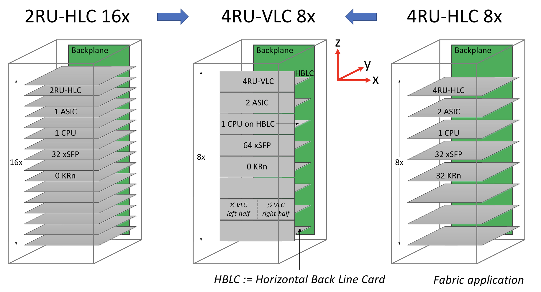
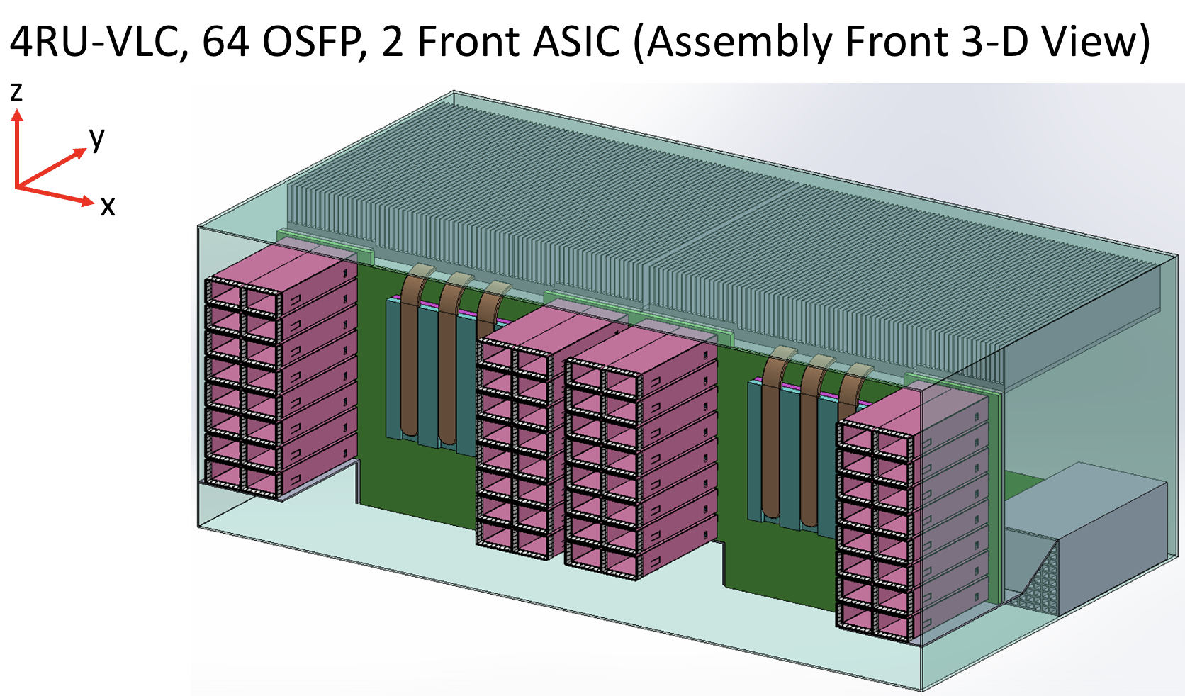
Vertical line card
The vertical line card design is 4RU high. Each card supports two ASICs on one side and 64 cages for the OSFP modules on the other.
A 32RU chassis can thus support eight vertical cards or 16 ASICs, equivalent to the chassis with 16 horizontal 2RU line cards.
The airflow for the ASICs is improved, enabling more moderate air fans to be used compared to 1RU or 2RU horizontal card chassis designs. There is also airflow across the modules.
“The key change in the architecture is the change from a horizontal card to a vertical card while maintaining the pluggable orientation,” says Cole.
As stated, the maximum distance between an ASIC and the pluggables is reduced to three inches, but Cole says the modules can be arranged around the ASIC to minimise the length to 2.5 inches.
Alternatively, if the height of the vertical card is an issue, a 3RU card can be used instead, which results in a maximum trace length of 3.5 inches. “[In this case], we don’t have dedicated air intakes for the CPU,” notes Cole.
Cole also mentioned the option of a 3RU vertical card that houses one ASIC and 64 OSFP modules. This would be suitable for the Tomahawk 5. However, here the maximum trace length is five inches.
Vertical connectors
Yamaichi Electronics has developed the vertical connectors needed to enable the design.
Cole points out that, unlike a horizontal connector, a vertical one uses equal-length contacts. This is not the case for a flat connector, resulting in performance degradation since a set of contacts has to turn and hence has a longer length.
Cole showed the simulated performance of an OSFP vertical connector with an insertion loss of over 70GHz.
“The loss up to 70GHz demonstrates the vertical connector advantage because it is low and flat for all the leads,” says Cole. “So this [design] is 200-gigabit ready.”
He also showed a vertical connector for the OSFP-XD with a similar insertion loss performance.
Also shown was a comparison with results published for Twinax cables. Cole says this indicates that the loss of a three-inch PCB trace is less than the loss of the cable.
“We’ve dramatically reduced the RF maximum length, so we had solved the RF roadblock problem, and we maintain the cost-benefit of horizontal line cards,” says Cole.
The I/O densities may be unchanged, but it preserves the mature technology’s benefits. “And then we get a dramatic improvement in cooling because there are no obstructions to airflow,” says Cole.
Vladimir Kozlov, CEO of the market research firm, LightCounting, wondered in a research note whether the vertical design is a distraction for the industry gearing up for co-packaged optics.
“Possibly, but all approaches for reducing power consumption on next-generation switches deserve to be tested now,” said Kozlov, adding that adopting co-packaged optics for Ethernet switches will take the rest of the decade.
“There is still time to look at the problem from all angles, literally,” said Kozlov

Lockheed Martin looks to pooling and optical I/O
Electronic systems must peer into ever-greater swathes of the electromagnetic spectrum to ensure a battlefield edge.
Michael HoffSuch electronic systems are used in ground, air, and sea vehicles and even in space.
The designs combine sensors and electronic circuitry for tasks such as radar, electronic warfare, communications and targeting.
Existing systems are custom designs undertaking particular tasks. The challenge facing military equipment makers is that enhancing such systems is becoming prohibitively expensive.
One proposed cost-saving approach is to develop generic radio frequency (RF) and sensor technology that can address multiple tasks.
“Now, each sensor will have to satisfy the requirements for all of the backend processing,” says Michael Hoff, senior research engineer at Lockheed Martin Advanced Technology Laboratories.
Such hardware will be more complex but upgrading systems will become simpler and cheaper. The generic sensors can also be assigned on-the-fly to tackle priority tasks as they arise.
“This is a foundational architectural shift that we see having relevance for many applications,” says Hoff.
Generic sensing
The proposed shift in architectural design was discussed in a paper presented at the IEEE International Symposium on Phased Array Systems and Technology event held in October.
Co-authored by Lockheed Martin and Ayar Labs, the paper focuses on generic sensing and the vast amount of data it generates.
Indeed, the data rates are such that optical interconnect is needed. This is where Ayar Labs comes in with its single-die electro-optical I/O chiplet.
Lockheed Martin splits sensing into two categories: RF sensing and electro-optic/ infrared (or EO/IR). Electro-optic sensors are used for such applications as high-definition imaging.
“When we talk about platform concepts, we typically lump EO/IR into one category,” says Hoff. The EO/IR could be implemented using one broadband sensor or with several sensors, each covering specific wavelengths.
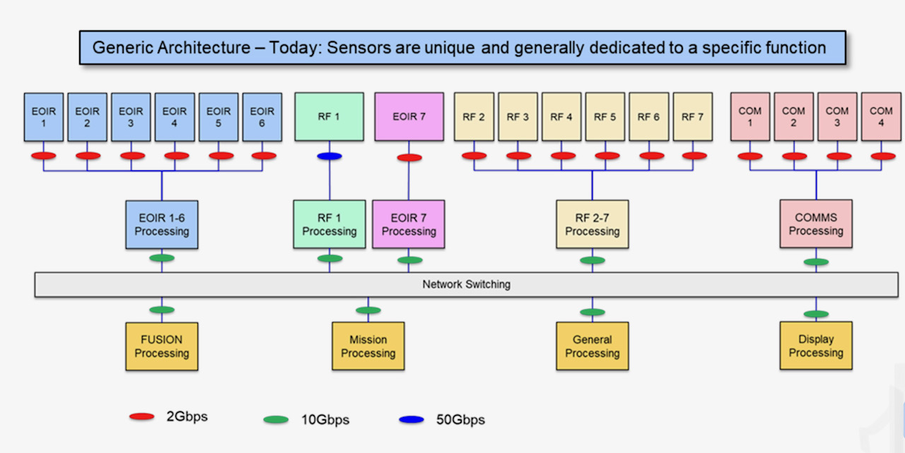
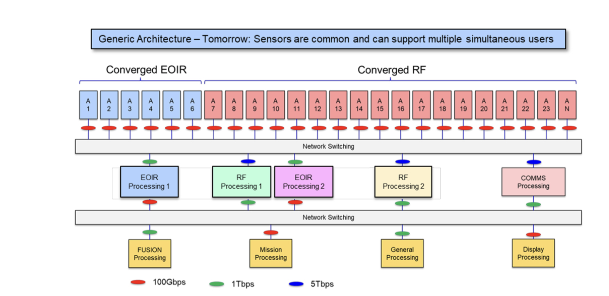
A representation of current systems is shown above. Here, custom designs comprising sensors, analogue circuitry, and processing pass data to mission-processing units. The mission equipment includes data fusion systems and displays.
Lockheed Martin proposed architecture uses two generic sensor types – RF and EO/IR – which can be pooled as required (see diagram below).
For example, greater resources may need to be diverted urgently to the radar processing at the expense of communications that can be delayed.
“It’s a more costly individual development, but because it can be shared across different applications and in different teams, cost savings come out ahead,” says Hoff.
An extra networking layer is added to enable the reconfigurability between the sensors and the mission functions and processing systems that use, process, and digest the dat
Optical interconnect
Data traffic generated by modern military platforms continues to rise. One reason is that the frequencies sensed are approaching millimetre-wave. Another is that phased-array systems are using more elements so that more data streams must be be digitised and assessed.
Lockheed Martin cites as an example a military platform comprising 16 phased-array antennas, each with 64 elements.
Each element is sampled with a 14-bit, 100 gigasample-per-second analogue-to-digital converter. The data rate is further doubled since in-phase and quadrature channels are sampled. Each phased array thus generates 179.2 terabits-per-second (Tbps) while the total system data is 2.87 petabits-per-second.
Algorithms at the sensor source can trim the raw data by up to 256x, reducing each antenna’s data stream to 700Gbps, or 11.2Tbps overall.
Optical communications is the only way to transport such vast data flows to the mission processors, says Lockheed Martin.
Multi-chip modules
Any interconnect scheme must not only transfer terabits of data but also be low power and compact.
“The size, weight and power constraints, whether an optical transceiver or processing hardware, get more constrained as you move towards the sensor location,” says Hoff.
The likelihood is that integrated photonics is going to be required as bandwidth demand increases and as the interconnect gets closer to the sensor, he says.
Lockheed Martin proposes using a multi-chip module design that includes the optics, in this case, Ayar Labs’s TeraPhy chiplet.
The TeraPhy combines electrical and silicon photonics circuitry on a single die. Overall, the die has eight transceiver circuits, each supporting eight wavelengths. In turn, each wavelength carries 32 gigabit-per-second (Gbps) of data such that the 54mm2 die transmits 2Tbps in total.
Lockheed Martin has compared its proposed multi-chip module design that includes integrated optics with a discrete solution based on mid-board optics.
The company says integrated optics reduced the power consumed by 5x, from 224W to 45W, while the overall area is reduced a dozen fold, from 3,527 mm2 to 295mm2.
“You’re going to need optical interconnects at many different points,” says Hoff; the exact locations of these multi-chip modules being design-dependent.
Charles Wuischpard, CEO of Ayar Labs, points out that the TeraPhy is built using macro blocks to deliver 2Tbps.
“There are customer opportunities that require far less bandwidth, but what they want is a very tiny chip with very low energy consumption on the input-output [I/O] transport,” says Wuischpard. “There are different areas where the size, weight and power benefits come into play, and it may not all be with our single chiplet solution that we offer.”
Investor
Lockheed Martin became a strategic investor in Ayar Labs in 2019.
“We see this [Ayar Labs’ optical I/O technology] as a foundational technology that we want to be out in front of and want to be first adopters of,” says Hoff.