
The market opportunity for linear drive optics
A key theme at OFC earlier this year that surprised many was linear drive optics. Its attention at the optical communications and networking event was intriguing because linear drive – based on using remote silicon to drive photonics – is not new.
“I spoke to one company that had a [linear drive] demo on the show floor,” says Scott Wilkinson, lead analyst for networking components at Cignal AI. “They had been working on the technology for four years and were taken aback; they weren’t expecting people to come by and ask about it. “
The cause of the buzz? Andy Bechtolsheim, famed investor, co-founder and chief development officer of network switching firm Arista Networks and, before that, a co-founder of Sun Microsystems.
“Andy came out and said this is a big deal, and that got many people talking about it,” says Wilkinson, author of a recent linear drive market research report.
Linear Drive
A data centre’s switch chip links to the platform’s pluggable optics via an electrical link. The switch chip’s serialiser-deserialiser (serdes) circuitry drives the signal across the printed circuit board to the pluggable optical module. A digital signal processor (DSP) chip inside the pluggable module cleans and regenerates the received signal before sending it on optically.
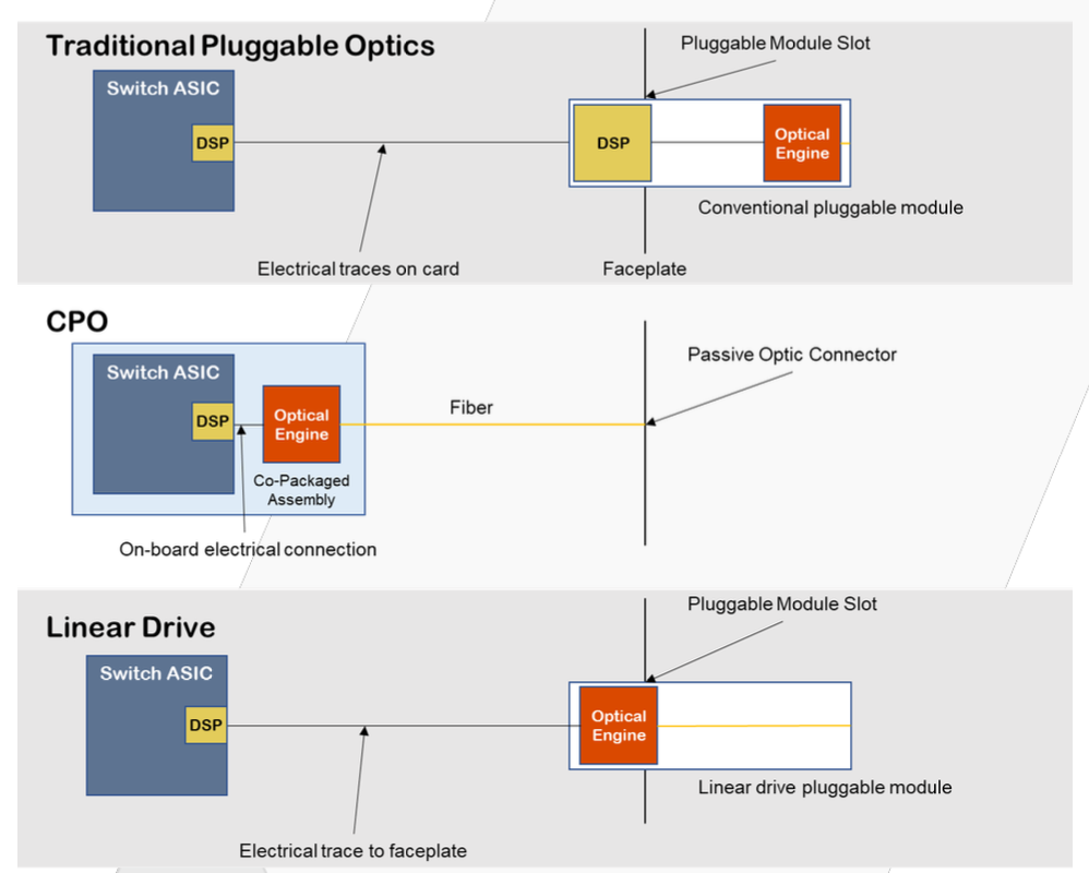
With linear drive optics, the switch ASIC’s serdes directly drives the module optics, removing the need for the module’s DSP chip. This cuts the module’s power consumption by half.
The diagram above contrasts linear drive optics compared with traditional pluggables and the emerging technology of co-packaged optics where the optics are adjacent to the switch chip and are packaged together. Linear drive optics can be viewed as a long-distance variant of co-packaged optics that comntinues to advance pluggable modules.
Proponents of linear drive claim that the power savings are a huge deal. “There will probably also be some cost savings, but it is not entirely clear how big they will be,” says Wilkinson. “But the only thing people want to discuss is the power savings.”
Misgivings
If linear drive’s main benefit is reducing power consumption, the technology’s sceptics counter with several technical and business issues.
One shortfall is that a module’s electrical and optical lanes must match in number and hence data rate. If there is a mismatch, the signal speeds must be translated between the electrical and optical lane rates, known as gearboxing. This task requires a DSP. Linear drive optics is thus confined to 800-gigabit optical modules: 800GBASE-DR8 and 800-gigabit 2xFR4. “There are people who think that at least 800 Gig – eight lanes in and eight lanes out – will continue to exist for a long time,” says Wilkinson.
Another question mark concerns the use of optics for artificial intelligence workloads. Adopters of AI will be early users of 200 gigabit-per-lane optics, requiring a gearbox-performing DSP.
Moreover, the advent of 200-gigabit electrical lanes will challenge serdes developers and, hence, linear drive designs. “It will be a technical challenge, the distances will be shorter, and some think it may never work,” says Wilkinson. “No matter how good the serdes is, it will not be easy.”
Co-packaged optics will also hit its stride once 200-gigabit serdes-based switch chips become available.
Another argument is that there are many ways to save power in the data centre; if linear drive introduces complications, why make it a priority?
Linear drive optics requires the switch chip vendors to develop high-quality serdes. Wilkinson says the leading switch vendors remain agnostic to linear drive, which is not a ringing endorsement. And while hyperscalers are investing time and resources into linear-drive technology, none have endorsed the technology such that they can withdraw at any stage without penalty.
“There is one story for linear drive and many stories against it,” admits Wilkinson. “When you compile them, it’s a pretty big story.”
Market opportunity
Cignal AI believes linear-drive optics will prove a niche market, with 800-gigabit linear-drive modules capturing 10 per cent of overall 800-gigabit pluggable shipments in 2027.
Wilkinson says the most promising example of the technology is active optical cables, where the modules and cables are a closed design. And while many companies are invested in the technology, and it will be successful, the opportunity will not be as significant as the proponents hope.

Agent of change

Dave Welch on how entrepreneurial problem-solving skills can tackle some of society’s biggest challenges
Dave Welch is best known for being the founder and chief innovation officer at Infinera, the optical equipment specialist. But he has a history of involvement in social causes.
In 2012, Welch went to court to fight for the educational rights of children in schools in California, a story covered by newspapers in the US and abroad and featured on the front cover of Time magazine.
“Ultimately, we lost,” says Welch. “But the facts of these [school] practices and their link to a poor educational outcome were confirmed and never disputed.”
Welch recently co-founded NosTerra Ventures, a non-profit organisation tackling challenging social issues. These Grand Challenges, as NosTerra calls them, cover housing, energy and environment, access to healthcare, public education, democracy, and information security, issues more suited to a presidential debate.
“NosTerra aims to identify key societal issues to contribute to, identify differentiated strategies and appropriate entrepreneurs, and help get those launched,” explains Welch. Nosterra has added partners, equivalent to a board of directors, to guide the organisation and ensure its strategies make sense. “We are not a Bill Gates or a Michael Bloomberg, but the object, frankly, is to make an organisation that can have the same influence on how we address these problems,” says Welch.
Welch says his involvement stems from being gifted with various opportunities, creating a responsibility to the greater society. Moreover, these issues define the quality of a society, so it is crucial to address them. “It’s also personally very rewarding to figure out what you can do to help,” says Welch.
Strategy for change
NosTerra works to identify what it must do to contribute to a solution and do it in a differentiated fashion, to make a structural change that improves things over time.
Welch returns to the example of public education and establishing the right to a quality education. “That’s a doable task, and trust me, we will reach out to the Bloombergs and the Gates to ask them for their help,” says Welch.
Energy and the environment is another example. Welch says there is much debate about the topic, which is only right given its impact. But less is discussed about the future direction of energy.
Welch sits on the Natural Resources Defense Council board, an important non-profit organisation, and is involved in setting strategies. He believes NosTerra can pursue various activities, including investing in technologies or creating the opportunity for its partners to invest directly. “In this case, the vehicles of change are that we absolutely need new technologies,” he says, citing the extreme example of fusion to shorter-term battery technologies.
NosTerra also believes it can use politics and influence what Welch calls factual prioritisation Developing solutions to significant problems by 2035 results in a markedly different approach to a 2060 timeframe. “If I’m a government or organisation, where do I want to spend my next pile of money?” says Welch. “What is shocking is that there isn’t a go-to validated model to run such scenarios on.”
Some organisations, such as the US Department of Energy, do have detailed models, but there is no open-source trusted model to see what impact short-term and longer-term investments will have. NosTerra is looking to address this with an open-source energy model so that if the Government is willing to invest $100 billion, it can identify what will give it the best return.
“I applaud the financial attack on the system to convert our energy sources, but I’m also a little appalled at the prioritisation of some of where we spend our money,” says Welch. “We can do some things to help there.”
NosTerra is busy creating a community around these areas to develop solutions to get ‘some of these things done’. Any NosTerra success will not be evident in one or two years but more likely five or ten years.
Welch stresses such ventures is not new to Silicon Valley. “David Packard and Bill Hewlett, those guys not only ran an incredible company [Hewlett-Packard or HP], but they were plugged into their community and sat on school boards,” he says. “I still find Silicon Valley is made up of people that care and work with the community.”
Welch is still fully involved at Infinera. “My added value [at Infinera] is the 40 years of watching telecom technologies develop and watching markets change,” he says. He provides creative thought, a perspective on technologies and why customers and markets will adopt specific directions. He also helps with prioritising what technologies Infinera should develop that will make a difference.
“I love that area,” he says.

The long arm of PCI Express
- Optical is being added as a second physical medium to the PCI Express (PCIe) data transfer protocol.
- PCI Express is an electrical standard, but now the Peripheral Component Interconnect Special Interest Group (PCI-SIG) has created a working group to standardise PCIe’s delivery optically.
- PCI-SIG is already developing copper cabling specifications for the PCI Express 5.0 and 6.0 standards.
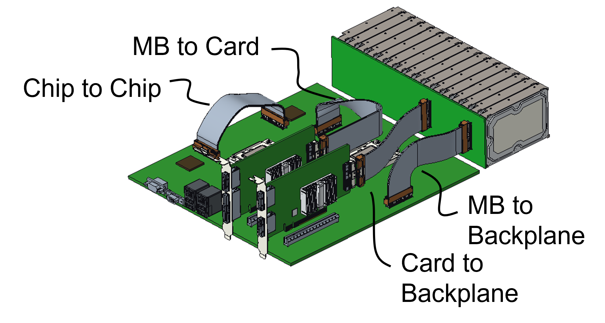
Since each generation of PCIe doubles the data transfer rate, PCI-SIG member companies want copper cabling to help with the design of high-speed PCIe interconnects on a printed circuit board (PCB), between PCBs, and between racks (see diagram).
“We’ve seen a lot of interest over recent months for an optical cable that will support PCI Express,” says Al Yanes, PCI-SIG president and chairperson.
He cites the trends of the decreasing cost and size of optics and how silicon photonics enables the adding of optics alongside ASICs.
“We have formed a workgroup to deliver an optical cable,” says Yanes. “There are many applications, but one is a longer-distance reach for PCI Express.”
“It is a void in the market [the lack of optical support for PCIe], and it needs to be filled,” says Bill Koss, CEO of Drut Technologies. “These efforts tend to take longer than estimated, so better to start sooner.”
Drut has developed a PCIe over photonics solution as part of its photonic direct connect fabric for the data centre.
The data centre is going photonic, says Koss, so there is a need for such working standards as photonics get closer to processors.
The PCIe protocol
PCIe is used widely across many industries.
In the data centre, PCIe is used by general-purpose microprocessors and accelerator chips, such as FPGAs, graphics processing units and AI hardware, to connect to storage and network interface cards.
The PCIe bus uses point-to-point communications based on a simple duplex scheme – serial transmissions in both directions which is referred to as a lane.
The bus can be bundled in various lane configurations – x1, x2, x4, x8, x12, x16 and x32 – with x4, x8 and x16 the configurations most used.
The first two PCIe versions, 1.0 and 2.0, delivered 2.5 and 5 giga transfers-per-second (GT/s) per lane per direction, respectively.
A transfer refers to an encoded bit. The first two PCIe versions use an 8b/10b encoding scheme such that for every ten-bit payload sent, 8 bits are data. This is why the data transfer rates per lane per direction are 2Gbps and 4Gbps (250 and 500 gigabytes per second), respectively.
With PCIe 3.0, the decision was made to increase the transfer rate to 8GT/s per lane, which assumed that no equalisation would be needed to counter inter-symbol interference at that speed. However, equalisation was required, which explains why PCIe 3.0 adopted 8GT/s and not 10GT/s.
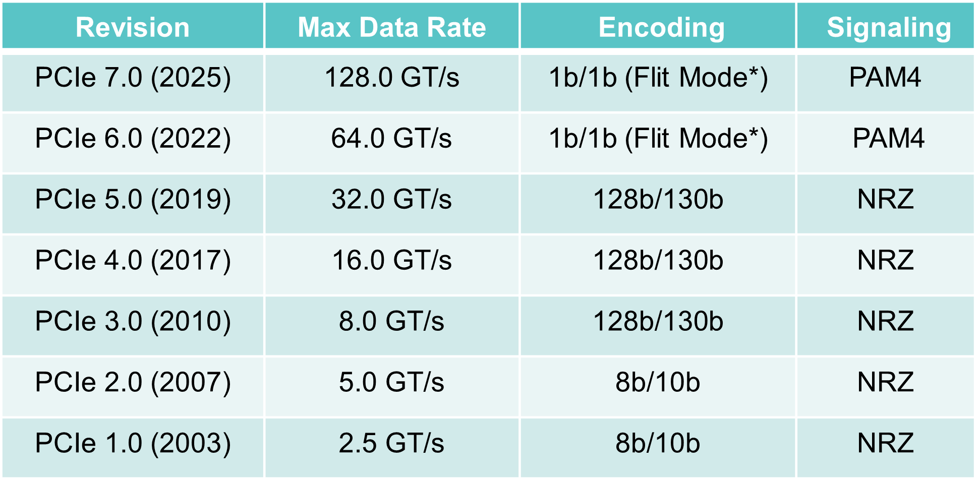
Another PCIe 3.0 decision was to move to a 128b/130b scheme to reduce the encoding overhead from 20 per cent to over 1 per cent. Now the transfer and bit rates are almost equal from the PCIe 3.0 standard onwards.
PCIe 4.0 doubles the transfer rate from 8GT/s to 16GT/s, while PCIe 5.0 is 32GT/s per lane per direction.
Since then, PCIe 6.0 has been specified, supporting 64GT/s per lane per direction. PCIe 6.0 is the first standard for 4-level pulse amplitude modulation (PAM4) signalling.
Now the PCIe 7.0 specification work is at version 0.3. PCIe 7.0 uses PAM-4 to deliver 128GT/s per lane per direction. The standard is expected to be completed in 2025, with industry adoption in 2027.
Optical cabling for PCIe
The PCI Express 5.0 and 6.0 copper cabling specifications are expected by the year-end. The expected distance using copper cabling and retimers is 5-6m.
The reach of an optical PCIe standard will ‘go a lot further’ than that, but how far is to be determined.
Yanes says optical cables for PCIe will also save space: “An optical cable is not as bulky nor as thick as a copper cable.”
Whether the optical specification work will support all versions of PCIe is to be determined.
“There’s some interest to support them all; the copper solution supports all the negotiations,” says Yanes. “It’s something that needs to be discussed, but, for sure, it will be the higher speeds.”
The working group will decide what optical options to specify. “We know that there are some basic things that we need to do to PCI Express technology to make it support optics,” says Yanes.
The working group aims to make the specification work generic enough that it is ‘optical friendly’.
“There are many optical techniques in the industry, and there is discussion as to which of these optical techniques is going to be the winner in terms of usage,” says Yanes. “We want our changes to make PCI Express independent of that discussion.”
The organisation will make the required changes to the base specification of PCIe to suit optical transmission while identifying which optical solutions to address and build.
PCI-SIG will use the same Flit Mode and the same link training, for example, while the potential specification enhancements include coordinating speed transitions to match the optics, making side-band signals in-band, and making the specification more power-efficient given the extended reach.
Pluggable optical modules, active optical cables, on-board optics, co-packaged optics and optical input-output are all optical solutions being considered.
An optical solution for PCIe will also benefit technologies such as Compute Express Link (CXL) and the Non-Volatile Memory Express (NVMe) protocols implemented over PCIe. CXL, as it is adopted more broadly, will likely drive new uses that will need such technology.
The PCIe optical working group will complete the specifications in 12-18 months. Yanes says a quicker working solution may be offered before then.

From 8-bit micros to modelling the brain
Part 1: An interview with computer scientist, Professor Steve Furber
Steve Furber is renowned for architecting the 32-bit reduced instruction set computer (RISC) processor from Acorn Computer, which became the founding architecture for Arm.
Arm processors have played a recurring role in Furber’s career. He and his team developed a clockless – asynchronous – version of the Arm, while a specialist Arm design has been the centrepiece building block for a project to develop a massively-parallel neural network computer.
Origins
I arrive at St Pancras International station early enough to have a coffee in the redeveloped St Pancras Renaissance London Hotel, the architecturally striking building dating back to the 19th century that is part of the station.
The train arrives on time at East Midlands Parkway, close to Nottingham, where Professor Steve Furber greets me and takes me to his home.
He apologises for the boxes, having recently moved to be closer to family.
We settle in the living room, and I’m served a welcome cup of tea. I tell Professor Furber that it has been 13 years since I last interviewed him.
Arm architecture
Furber was a key designer at Acorn Computer, which developed the BBC Microcomputer, an early personal computer that spawned a generation of programmers.
The BBC Micro used a commercially available 8-bit microprocessor, but in 1983-84 Acorn’s team, led by Furber, developed a 32-bit RISC architecture.
The decision was bold and had far-reaching consequences: the Acorn RISC Machine, or ARM1, would become the founding processor architecture of Arm.
Nearly 40 years on, firms have shipped over 250 billion Arm-based chips.
Cambridge
Furber’s interest in electronics began with his love of radio-controlled aircraft.
He wasn’t very good at it, and his Physics Master at Manchester Grammar School helped him.
Furber always took a bag with him when flying his model plane, as he often returned with his plane in pieces; he refers to his aircraft as ‘radio-affected’ rather than radio-controlled.
Furber was gifted at maths and went to Cambridge, where he undertook the undergraduate Mathematical Tripos, followed by the Maths Part III. Decades later, the University of Cambridge recognised Maths Part III as equivalent to a Master’s.
“It [choosing to read maths] was very much an exploration,” says Furber. “My career decisions have all been opportunistic rather than long-term planned.”
At Cambridge, he was influenced by the lectures of British mathematician James Lighthill on biofluid dynamics. This led to Furber’s PhD topic, looking at the flight of different animals and insects to see if novel flight motions could benefit jet-engine design.
He continued his love of flight as a student by joining a glider club, but his experience was mixed. When he heard of a fledgling student society building computers, he wondered if he might enjoy using computers for simulated flight rather than actual flying.
“I was one of the first [students] that started building computers,” says Furber. “And those computers then started getting used in my research.”
The first microprocessor he used was the 8-bit Signetics 2650.
Acorn Computers
Furber’s involvement in the Cambridge computer society brought him to the attention of Chris Curry and Hermann Hauser, co-founders of Acorn Computers, a pioneering UK desktop company.
Hauser interviewed and recruited Furber in 1977. Furber joined Acorn full-time four years later after completing his research fellowship.
Hauser, who co-founded venture capital firm Amadeus Capital Partners, said Furber was among the smartest people he had met. And having worked in Cambridge, Hauser said he had met a few.
During design meetings, Furber would come out with outstandingly brilliant solutions to complex problems, said Hauser, who led the R&D department at Acorn Computers.
BBC Micro and the ARM1
The BBC’s charter was to educate the public and broadcast programmes highlighting microprocessors.
The UK broadcaster wanted to educate in detail about what microprocessors might do and was looking for a computer to provide users with a hands-on perspective via TV programmes.
When the BBC spoke to Acorn, it estimated it would need 12,000 machines. Public demand was such that 1.5 million Acorn units were sold.
The computer’s success led Acorn to consider its next step. Acorn had already added a second processor to the BBC Micro, and Acorn had expanded its computer portfolio, including the Acorn Cambridge workstation. But by then, microprocessors were moving from 8-bit to 16-bits.
Acorn’s R&D group lab-tested leading 16-bit processors but favoured none.
One issue was that the processors would not be interruptible for relatively long periods – when writing to disk storage, for example, yet the BBC Micro used processor interrupts heavily.
A second factor was that memory chips accounted for much of the computer’s cost.
“The computer’s performance was defined by how much memory bandwidth the processor could access, and those 16-bit processors couldn’t use the available bandwidth; they were slower than the memory,” says Furber. “And that struck us as just wrong.”
While Furber and colleagues were undecided about how to proceed, they began reading academic papers on RISC processors, CPUs designed on principles different to mainstream 16-bit processors.
“To us, designing the processor was a bit of a black art,” says Furber. “So the idea that there was this different approach, which made the job much simpler, resonated with us.”
Hauser was very keen to do ambitious things, says Furber, so when Acorn colleague, Sophie Wilson, started discussing designing a RISC instruction set, they started work but solely as an exploration.
Furber would turn Wilson’s processor instructions and architecture designs into microarchitecture.
“It was sketching an architecture on a piece of paper, going through the instructions that Sophie had specified, and colouring it in for what would happen in each phase,” says Furber.
The design was scrapped and started again each time something didn’t work or needed a change.
“In this sort of way, that is how the ARM architecture emerged,” says Furber.
It took 18 months for the first RISC silicon to arrive and another two years to get the remaining three chips that made up Acorn’s Archimedes computer.
The RISC chip worked well, but by then, the IBM PC had emerged as the business computer of choice, confining Acorn to the educational market. This limited Acorn’s growth, making it difficult for the company to keep up technologically.
Furber was looking at business plans to move the Arm activity into a separate company.
“None of the numbers worked,” he says. “If it were going to be a royalty business, you’d have to sell millions of them, and nobody could imagine selling such numbers.”
During this time, a colleague told him how the University of Manchester was looking for an engineering professor. Furber applied and got the position.
Arm was spun out in November 1990, but Furber had become an academic by then.

Asynchronous logic
Unlike most UK computing departments, Manchester originated in building machines. Freddy Williams and Tom Kilburn built the first programmed computer in 1948. Kilburn went on to set up the department.
“The department grew out of engineering; most computing departments grew out of Maths,” says Furber.
Furber picked asynchronous chip design as his first topic for research, motivated by a desire to improve energy efficiency. “It was mainly exploring a different way to design chips and seeing where it went,” says Furber.
Asynchronous or self-timed circuits use energy only when there’s something useful to do. In contrast, clocked circuits burn energy all the time unless they turn their clocks off, a technique that is now increasingly used.
Asynchronous chips also have significant advantages in terms of electromagnetic interference.
“What a clock does on the chip is almost as bad as you can get when it comes to generating electrical interference, locking everything to a particular frequency, and synchronising all the current pulses is exactly that,” says Furber.
The result was the Amulet processor series, asynchronous versions of the Arm, which kept Furber and his team occupied during the 1990s and the early 2000s.
In the late 1990s, Arm moved from making hard-core processors to synthesised ones. The issue was that the electronic design automation (EDA) tools did not synthesise asynchronous designs well.
While Furber and his team learnt how to build chips – the Amulet3 processor was a complete asynchronous system-on-chip – the problem shifted to automating the design process. Even now, asynchronous design EDA tools are lagging, he says.
In the early 2000s, Furber’s interest turned to neuromorphic computing.
The resulting SpiNNaker chip, the programable building block of Furber’s massively parallel neural network, uses asynchronous techniques, as does Intel’s Loihi neuromorphic processor.
“There’s always been a synergy between neuromorphic and asynchronous,” says Furber.
Implementing a massive neural network using specialised hardware has been Furber’s main interest for the last 20 years, the subject of the second part of the interview.
For Part 2: Modelling the Human Brain with specialised CPUs, click here
Further Information:
The Everything Blueprint: The Microchip Design That Changed The World, by James Ashton.

Modelling the Human Brain with specialised CPUs

Part 2: University of Manchester’s Professor Steve Furber discusses the design considerations for developing hardware to mimic the workings of the human brain.
The designed hardware, the Arm-based Spiking Neural Network Architecture (SpiNNAker) chip, is being used to understand the working of the brain and for industrial applications to implement artificial intelligence (AI)
Steve Furber has spent his career researching computing systems but his interests have taken him on a path different to the mainstream.
As principal designer at Acorn Computers, he developed a reduced instruction set computing (RISC) processor architecture when microprocessors used a complex instruction set.
The RISC design became the foundational architecture for the processor design company Arm.
As an academic, Furber explored asynchronous logic when the digital logic of commercial chips was all clock-driven.
He then took a turn towards AI during a period when AI research was in the doldrums.
Furber had experienced the rapid progress in microprocessor architectures, yet they could not do things that humans found easy. He became fascinated with the fundamental differences between computer systems and biological brains.
The result was a shift to neuromorphic computing – developing hardware inspired by neurons and synapses found in biological brains.
The neural network work led to the Arm-based SpiNNaker and the University of Manchester’s massively parallel computer that uses one million.
Now, a second-generation SpiNNaker exists, a collaboration between the University of Manchester and University of Technology Dresden. But it is Germany, rather than the UK, exploiting the technology for its industry.
Associative memory
Furber’s interest in neural networks started with his research work on inexact associative memory.
Traditional memory returns a stored value when the address of a specific location in memory is presented to the chip. In contrast, associative memory – also known as content addressable memory – searches all of its store, returning data only when there is an exact match. Associative memory is used for on-chip memory stores for high-speed processors, for example.
Each entry in the associative memory effectively maps to a point in a higher dimensional space, explains Furber: “If you’re on that point, you get an output, and if you’re not on that point, you don’t.”
The idea of inexact associative memory is to soften it by increasing the radius at the output from a point to a space.
“If you have many of these points in space that you are sensitive to, then what you want to do is effectively increase the space that gives you an output without overlapping too much,” says Furber. “This is exactly what a neural network looks for.”
Biological neural networks
Neurons and synapses are the building blocks making up a biological neural network. A neuron sends electrical signals to a network of such cells, while the synapse acts as a gateway enabling one neuron to talk to another.
When Furber looked at biological neural networks to model them in hardware, he realized the neural networks models kept changing as the understanding into their workings deepened.
So after investigating hardware designs to model biological neural networks, he decided to make the engines software programmable. Twenty years on, the decision proved correct, says Furber, allowing the adaptation of the models run on the hardware.
Furber and his team chose the Arm architecture to base their programmable design, resulting in the SpiNNaker chip.
SpiNNaker was designed with massive scale in mind, and one million SpiNNakers make up the massively parallel computer that models human brain functions and runs machine learning algorithms.
Neurons, synapses and networking
Neural networks had a low profile 20 years ago. It was around 2005 when academic Geoffrey Hinton had a breakthrough that enabled deep learning to take off. Hinton joined Google in 2013 and recently resigned from the company to allow him to express his concerns about AI.
Furber’s neural network work took time; funding for the SpiNNaker design began in 2005, seven years after the inexact associative memory began.
Furber started by looking at how to model neural networks in hardware more efficiently: neurons and synapses.
“The synapse is a complex function which, my biological colleagues tell me, has 1,500 proteins; the presence or absence of each affects how it behaves,” says Furber. “So you have very high dimensional space around one synapse in reality.”
Furber and his team tackled such issues as how to encode the relevant equations in hardware and how the chips were to be connected, given the connectivity topology of the human brain is enormous.
A brain neuron typically connects to 10,000 others. Specific cells in the cerebellum, a part of the human brain that controls movement and balance, have up to 250,000 inputs.
“How do they make a sensible judgment, and what’s happening on these quarter of a million impulses is a mystery,” says Furber.
SpiNNaker design
Neurons communicate by sending electrical spikes, asynchronous events that encapsulate information in the firing patterns, so the SpiNNaker would have to model such spiking neurons.
In the human brain, enormous resources are dedicated to communication; 100 billion (1011) neurons are linked by one quadrillion (1015) connections.
For the chip design, the design considerations included how the inputs and outputs would get into and out of the chip and how the signals would be routed in a multi-chip architecture.
Moreover, each chip would have to be general purpose and scalable so that the computer architecture could implement large brain functions.
Replicating the vast number of brain connections electronically is impractical, so Furber and his team exploited the fact that electronic communication is far faster than the biological equivalent.
This is the basis of SpiNNaker: electrical spikes are encapsulated as packets and whizzed across links. The spikes reach where they need to be in less than a millisecond to match biological timescales.
The neurons and synapses are described using mathematical functions solved on the Arm-based processor using fixed-point arithmetic.
SpiNNaker took five years to design. This sounds a long time, especially when the Arm1 took 18 months, until Furber explains the fundamental differences between the two projects.
“Moore’s Law has delivered transistors in exponentially growing abundance,” he says. “The Arm1 had 25,000 transistors, whereas the SpiNNaker has 100 million.”
Also, firms have tens or even 100s of engineers designing chips; the University of Manchester’s SpiNNaker team numbered five staff.
One critical design decision that had to be made was whether a multi-project wafer run was needed to check SpiNNaker’s workings before committing to production.
“We decided to go for the full chip, and we got away with it,” says Furber. Cutting out the multi-project wafer stage saved 12% of the total system build cost.
The first SpiNNaker chips arrived in 2010. First test boards had four SpiNNaker chips and were used for software development. Then the full 48-chip boards were made, each connecting to six neighbouring ones.

The first milestone was in 2016 when a half-million processor machine was launched and made available for the European Union’s Human Brain Project. The Human Brain Project came about as an amalgam of two separate projects; modelling of the human brain and neuromorphic computing.
This was followed in 2018 by the entire one million SpiNNaker architecture.
“The size of the machine was not the major constraint at the time,” says Furber. “No users were troubled by the fact that we only had half a million cores.” The higher priority was improving the quality and reach of the software.
Programming the computer
The Python programming language is used to program the SpiNNaker parallel processor machine, coupled with the Python Neural Network application programming interface (PyNN API).
PyNN allows neuroscientists to describe their networks as neurons with inputs and outputs (populations) and how their outputs act as inputs to the next layer of neurons (projections).
Using this approach, neural networks can be described concisely, even if it is a low-level way to describe them. “You’re not describing the function; you’re describing the physical instantiation of something,” says Furber.
Simulators are available that run on laptops to allow model development. Once complete, the model can be run on the BrainScaleS machine for speed or the SpiNNaker architecture if scale is required.
BrainScaleS, also part of the Human Brain Project, is a machine based in Heidelberg, Germany, that implements models of neurons and synapses at 1000x biological speeds.
Modeling the brain
The SpiNNaker computer became the first to run a model of the segment of a mammalian cortex in real biological time. The model of the cortex was developed by Jülich Research Centre in Germany.
“The cortex is a very important part of the brain and is where most of the higher-level functions are thought to reside,” says Furber.
When the model runs, it reproduces realistic biological spiking in the neural network layers. The problem, says Furber, is that the cortex is poorly understood.
Neuroscientists have a good grasp of the Cortex’s physiology – the locations of the neurons and their connections, although not their strengths – and this know-how is encapsulated in the PyNN model.
But neuroscientists don’t know how the inputs are coded or what the outputs mean. Furber describes the Cortex as a black box with inputs and outputs that are not understood.
“What we are doing is building a model of the black box and asking if the model is realistic in the sense that it reproduces something we can sensibly measure,” says Furber
For neuroscientists to progress, the building blocks must be combined to form whole brain models to understand how to test them.
At present, the level of testing is to turn them on and see if they produce realistic spike patterns, says Furber.

SpiNNaker 2
A second-generation SpiNNaker 2 device has been developed, with the first silicon available in late 2022 while the first large SpiNNaker 2 boards are becoming available.
The original SpiNNaker was implemented using a 130nm CMOS process, while SpiNNaker 2 is implemented using a 22nm fully depleted silicon on insulator (FDSOI) process.
SpiNNaker 2 improves processing performance by 50x such that a SpiNNaker 2 chip exceeds the processing power of the 48- SpiNNaker printed circuit board.
SpiNNaker 2’s design is also more general purpose. A multiply-accumulator engine has been added for deep learning AI. The newer processor also has 152 processor engines compared to Spinnaker’s 18, and the device includes dynamic power management.
“Each of the 152 processor engines effectively has its dynamic voltage and frequency scaling control,” says Furber. “You can adjust the voltage and frequency and, therefore, the efficiency for each time step, even at the 0.1-millisecond level; you look at the incoming workload and just adjust.”
The University of Technology Dresden has been awarded an $8.8 billion grant to build a massively parallel processor using 10 million SpiNNaker 2 devices.
The university is also working with German automotive firms to develop edge-cloud applications using SpiNNaker 2 to process sensor data with milliseconds latency.
The device is also ideal for streaming AI applications where radar, video or audio data can be condensed close to where it is generated before being sent for further processing in the cloud.
Furber first met with the University of Technology Dresden’s neuromorphic team via the Human Brain Project.
The teams decided to collaborate, given Dresden’s expertise in industrial chip design complementing Furber and his team’s system expertise.
Takeaways
“We are not there yet, says Furber, summarizing the brain work in general.
Many practical lessons have been learnt from the team’s research work in developing programmable hardware at a massive scale. The machine runs brain models in real time, demonstrating realistic brain behaviour.
“We’ve built a capability,” he says. “People are using this in different ways: exploring ideas and exploring new learning rules.
In parallel, there has also been an explosion in industrial AI, and a consensus is emerging that neuromorphic computing and mainstream AI will eventually converge, says Furber.
“Mainstream AI has made these huge advances but at huge cost,” says Furber. Training one of these leading neural networks takes several weeks consuming vast amounts of power. “Can Neuromorphics change that?”
Mainstream AI is well established and supported with compelling tools, unlike the tools for neuromorphic models.
Furber says the SpiNNaker technology is proven and reliable. The Manchester machine is offered as a cloud service and remained running during the pandemic when no one could enter the university.
But Furber admits it has not delivered any radical new brain science insights.
“We’ve generated the capability that has that potential, but no results have been delivered in this area yet, which is a bit disappointing for me,” he says.
Will devices like SpiNNaker impact mainstream AI?
“It’s still an open question,” says Furber. “It has the potential to run some of these big AI applications with much lower power.”
Given such hardware is spike-driven, it only processes when spiking takes place, saving energy. As does the nature of the processing, which is sparse, areas of the chip tend to be inactive during spiking.
Professor Emeritus
Furber is approaching retirement. I ask if he wants to continue working as a Professor Emeritus. “I hope so,” he says. “I will probably carry on at that moment.”
He also has some unfinished business with model aircraft. “I’ve never lost my itch to play with model aeroplanes, maybe I’ll have time for that,” he says.
The last time he flew planes was when he was working at Acorn. “Quite often, the aeroplanes came back in one piece,” he quips.
For Part 1: From 8-bit micros to the modeling the human brain, click here
Further information
Podcast: SpiNNaker 2: Building a Brain with 10 Million CPUs

The computing problem of our time: Moving data
- Celestial AI’s Photonic Fabric technology can deliver up to 700 terabits per second of bidirectional bandwidth per chip package.
- The start-up has recently raised $100 million in funding.
The size of AI models that implement machine learning continue to grow staggeringly fast.
Such AI models are used for computer vision, large language models such as ChatGPT, and recommendation systems that rank items such as search results and music playlists.
The workhorse silicon used to build such AI models are graphics processing units (GPUs). GPU processing performance and their memory size may be advancing impressively but AI model growth is far outpacing their processing and input-output [I/O] capabilities.
To tackle large AI model workloads, hundreds and even thousands of GPUs are deployed in parallel for boost overall processing performance and high-performance memory storage capacity.
But it is proving hugely challenging to scale such parallel systems and feed sufficient data to the expensive processing nodes so they can do their work.
Or as David Lazovsky, CEO of start-up Celestial AI puts it, data movement has become the computing problem of our time.
Input-output bottleneck
The data movement challenge and scaling hardware for machine learning has caused certain AI start-ups to refocus, looking beyond AI processor development to how silicon photonics can tackle the input-output [I/O] bottleneck.
Lightelligence is one such start-up; Celestial AI is another.
Founded in 2020, Celestial AI has raised $100 million in its latest round of funding, and $165 million overall.
Celestial AI’s products include the Orion AI processor and its Photonic Fabric, an optoelectronic system-in-package comprising a silicon photonics chip and the associated electronics IC.
The Photonic Fabric uses two technological differentiators: a thermally stable optical modulator, and an electrical IC implemented in advanced CMOS.

Thermally stable modulation
Many companies use a ring resonator modulator for their co-packaged optics designs, says Lazovsky. Ring resonator modulators are tiny but sensitive to heat, so they must be temperature-controlled to work optimally.
“The challenge of rings is that they are thermally stable to about one degree Celsius,” says Lazovsky.
Celestial AI uses silicon photonics as an interposer such that it sits under the ASIC, a large chip operating at high temperatures.
“Using silicon photonics to deliver optical bandwidth to a GPU that’s running at 500-600 Watts, that’s just not going to work for a ring,” says Lazovsky, adding that even integrating silicon photonics into memory chips that consume 30W will not work.
Celestial AI uses a 60x more thermally stable modulator than a ring modulator.
The start-up uses continuous wave distributed feedback laser (DFB) lasers as the light source, the same lasers used for 400-gigabit DR4 and FR4 pluggable transceivers, and sets their wavelength to the high end of the operating window.
The result is a 60-degree operating window where the silicon photonics circuits can operate. “We can also add closed-loop control if necessary,” says Lazovsky.
Celestial AI is not revealing the details of its technology, but the laser source is believed to be external to the silicon photonics chip.
Thus a key challenge is getting the modulator to work stably so close to the ASIC, and this Celestial AI says it has done.
Advanced CMOS electronics
The start-up says TSMC’s 4nm and 5nm CMOS are the process nodes to be used for the Photonic Fabric’s electronics IC accompanying the optics.
“We are qualifying our technology for both 4nm and 5nm,” says Lazovsky. “Celestial AI’s current products are built using TSMC 5nm, but we have also validated the Photonic Fabric using 4nm for the ASIC in support of our IP licensing business.”
The electronics IC includes the modulator’s drive circuitry and the receiver’s trans-impedance amplifier (TIA).
Celestial AI has deliberately chosen to implement the electronics in a separate chip rather than use a monolithic design as done by other companies. With a monolithic chip, the optics and electronics are implemented using the same 45nm silicon photonics process.
But a 45nm process for the electronics is already an old process, says the start-up.
Using state-of-the-art 4nm or 5nm CMOS cuts down the area and the power requirements of the modulation driver and TIA. The optics and electronics are tightly aligned, less than 150 microns apart.
“We are mirroring the layout of our drivers and TIAs in electronics with the modulator and the photodiode in silicon photonics such that they are directly on top of each other,” says Lazovsky.
The proximity ensures a high signal-to-noise ratio; no advanced forward error correction (FEC) scheme or a digital signal processor (DSP) is needed. The short distances also reduce latency.
This contrasts with co-packaged optics, where chiplets surround the ASIC to provide optical I/O but take up valuable space alongside the ASIC edge, referred to as beachfront.
If the ASIC is a GPU, such chiplets must compete with stacked memory packages – the latest version being High Bandwidth Memory 3 (HBM3) – that also must be placed close to the ASIC.
There is also only so much space for the HBM3’s 1024-bit wide interface to move data, a problem also shared by co-packaged optics, says Lazovsky.
Using the Universal Chiplet Interconnect Express (UCIe) interface, for example, there is a limit to the bandwidth that can be distributed, not just to the chip but across the chip too.
“The beauty of the Photonic Fabric is not just that we have much higher bandwidth density, but that we can deliver that bandwidth anywhere within the system,” says Lazovsky.
The interface comes from below the ASIC and can deliver data to where it is needed: to the ASIC’s compute engines and on-chip Level 2 cache memory.
Bandwidth density
Celestial AI’s first-generation implementation uses four channels of 56 gigabits of non-return-to-zero signalling to deliver up to 700 terabit-per-second (Tbps) total bidirectional bandwidth per package.
How this number is arrived have not been given, but it is based on feeding the I/O via the ASIC’s surface area rather than the chip’s edges.
To put that in perspective, Nvidia’s latest Hopper H100 Tensor Core GPU uses five HBM3 sites. These sites deliver 80 gigabytes of memory and over three terabytes-per-second – 30Tbps – total memory bandwidth.”
The industry trend is to add more HBM memory in-package, but AI models are growing hundreds of times faster. “You need orders of magnitude more memory for a single workload than can fit on a chip,” he says.
Accordingly, vast amounts of efficient I/O are needed to link AI processors to remote pools of high-bandwidth memory by disaggregating memory from compute.
Celestial AI is now working on its second-generation interface that is expected in 18 months. The newer interface quadruples the package bandwidth to >2,000Tbps. The interface uses 4-level pulse amplitude modulation (PAM-4) signaling to deliver 112Gbps per channel and doubles the channel count from four to eight.
“The fight is about bandwidth density, getting large-scale parameters from external memory to the point of computing as efficiently as possible,” says Lazovsky,
By efficiently, Lazovsky means bandwidth, energy, and latency. And low latency for AI applications translates to revenues.
Celestial AI believes its Photonics Fabric technology is game-changing due to the bandwidth density achieved while overcoming the beachfront issue.
Composible memory
Celestial AI changed its priorities to focus on memory disaggregation after working with hyperscalers for the last two years.
The start-up will use its latest funding to expand its commercial activities.
“We’re building optically interconnected, high-capacity and high-bandwidth memory systems to allow our customers to develop composable resources,” says Lazovsky.
Celestial AI is using its Photonic fabric to enable 16 servers (via PCI Express cards) to access a single high-capacity optical-enabled DDR, HBM and hybrid pooled memory.
Another implementation will use its technology in chiplet form via the UCIe interface. Here, the bandwidth is 14.4Tbps, more than twice the speed of the leading co-packaged optics solutions.
Celestial AI also has an optical multi-chip interconnect bridge (OMIB), enabling an ASIC to access pooled high-capacity external memory in a 40ns round trip. OMIB can also be used to link chips optically on a multi-chip module.
Celestial AI stressed that its technology is not limited to memory disaggregation. The Photonic Fabric came out of the company looking to scale multiples of its Orion AI processors.
Celestial AI supports the JEDEC HBM standard and CXL 2.0 and 3.0, as well as other physical interface technologies such as Nvidia’s NVlink and AMD’s Infinity fabric.
“It is not limited to our proprietary protocol,” says Lazovsky.
The start-up is in discussions with ‘multiple’ companies interested in its technology, while Broadcom is a design services partner. Near Margalit, vice president and general manager of Broadcom’s optical systems division, is a technical advisor to the start-up.
Overall, the industry trend is to move from general computing to accelerated computing in data centres. That will drive more AI processors and more memory and compute disaggregation.
“It is optical,” says Lazovsky: “There is no other way to do it.”

Using light to connect an AI processor’s cores
Lightelligence is using silicon photonics to connect 64 cores of its AI processor. But the company has bigger ambitions for its optical network-on-chip technology
Lightelligence has unveiled its optical network-on-chip designed to scale multiprocessor designs.
The start-up’s first product showcasing the technology is the Hummingbird, a system-in-package that combines Lightelligence’s 64-core artificial intelligence (AI) processor and a silicon photonics chip linking the processor’s cores.
A key issue impeding the scaling of computing resources is the ‘memory wall’ which refers to the growing gap between processor and memory speeds, causing processors to be idle as they wait for data to crunch.
“The memory wall is a genuine problem,” says Maurice Steinman, vice president of engineering at Lightelligence. “Even with the generational scaling of computing, the input-output (I/O) and access to off-chip communications are struggling to keep up.”
Lightelligence has developed Hummingbird to show how its optical networking approach could be used to scale multi-chip designs.
Origins
Lightelligence, an MIT spin-out, is a fabless chip company founded in 2017. The start-up has 200 engineers and has raised over $200 million in funding. Now, after five years, the company is beginning to generate revenues.
The company started by using nanophotonics to tackle such computations as matrix multiplications and linear algebra.
After two years, the focus broadened to include communications. There is no point in developing a low-latency analogue compute engine only to then encounter I/O and scaling issues, says Steinman.
Optical network-on-chip
The start-up is pursuing two communication tracks. The first is developing board-to-board or rack-to-rack communications based on optical transceivers and fibre. The second is communications at a smaller, system-in-package or chip-to-wafer scale, with Hummingbird and the optical network-on-chip being the first example.
“How do we address the challenges of purely electronic solutions today?” says Steinman. “How can we use photonics and an optical waveguide-based solution to get back some of the limitations there?”
The issue is that while chips can now have transistor counts in the tens of billions, a dimensions of the die are limited to some 800mm2, dictated by the reticule size. A multi-chip module or a chiplet approach is needed if additional computation is required.
“Ideally, you would want the performance to scale with the sum of silicon area; if I’ve got N chips, I want pure linear scaling,” says Steinman.
The issue with multiple chips is that they need interfaces which introduce communication and power consumption issues. And with an array of chips, a scheduler must oversee workload assignment to the processors as they become available.
“You’ve got all these interfaces, you’ve got queuing delay, you’ve got contention, you have multiple messages trying to contend for the same path,” says Steinman. “It is hard to see all that in multiple dimensions.”
Lightelligence wants to use optical networking to enable routing topologies linking compute resources that are impractical if attempted electronically.
“That’s the breakthrough we’re trying to bring to the world,” says Steinman. “What we are calling optical network-on-chip.”
The first implementation uses a network to link cores of a single-chip parallel processor, while the goal is to extend the networking beyond the chip scale, he says.
Lightelligence believes the technology will be attractive to silicon vendors facing similar scale-out issues. And by having a functioning device, the start-up has credibility when approaching potential customers.
“We want to work with them to design a purpose-built semi-custom solution because I’m sure every scale-out solution has different topology needs,” says Steinman.
Architecture
The Hummingbird device uses programmable cores that implement scalar, vector, and matrix operations, including 2D convolution. Such computations are accelerated using the optical network-on-chip with convolution used to implement a convolutional neural network for AI.
The chip includes a central instruction unit to implement a single-instruction, multiple-data (SIMD) architecture; each core performing the same operation on part of the data set.
To aid the computation, each core has an optical broadcast transmitter. Every core can send and also receive data from every other core using the silicon photonics chip’s splitters and optical waveguides.
The ratio used by the optical-network-on-chip is 64 optical transmitters and 512 optical receivers rather than 64×64 optical receivers. This simplifies the optical design’s complexity, with electronics being used for the final stage to get data to particular cores in eight-core clusters.
“It is an all-to-all broadcast, an unusual topology,” says Steinman. “But in doing that, we have put a lot of transmitters and receivers on our companion photonic die that goes with the electronic [AI processor] die in Hummingbird.”
Lightelligence says the silicon photonics chip could implement other topologies, such as a 2D torus, for example.
Benefits
The motivation for the Lightelligence design is to achieve linear scaling, beyond what Hummingbird is showing for the single chip design. That said, the design already shows that many optical transmitters and receivers can be integrated into a dense space.
Lightelligence’s approach is also pragmatic. It has taken several years to develop Hummingbird and the start-up didn’t want to wait before developing a wafer-scale solution.
“There’s a little bit of constraining the problem to a single die, which is not the optimal proof point for it,” says Steinman. “But now we have a tangible working thing that gives us credibility for those higher-scale conversations.”
Steinman says the limit using the optical-network-on-chip technology is a wafer-sized design. Scaling beyond a wafer will require conventional optical interface technology (oNET, see diagram below) which Lightelligence is also developing.
Customers
The start-up has developed a PCI Express (PCIe) plug-in card that hosts the Hummingbird system-in-package. “It is a programmable machine; it does have an instruction set, compiler, and toolchain,” says Steinman.
Samples are with early adopter customers with AI inference tasks and Lightelligence is awaiting their feedback. “That next level of feedback is really important for our commercial objectives,” says Steinman.
Lightelligence also wants to partner with chip companies to start working on what Steinman calls ‘semi-custom’ engagements. “What are their problems that need to be solved, and how can we help?” he says.
Lightelligence will demonstrate the Hummingbird at the Hot Chips 2023 event in late August at Stanford University. Details of the device’s performance will also be revealed.

Fibre to everywhere
For years, passive optical networks (PON) were all about fibre-to-the-premise, particularly fibre-to-the-home. Japan, South Korea, and China led the market with massive PON deployments.
“Now the focus is on fibre-to-everywhere, whether it’s a home, a business, a school, a university, an enterprise, a traffic light,” says Julie Kunstler, chief analyst, broadband access intelligence at Omdia.
Meanwhile, in the US, government funding is spurring fibre deployments, especially in underserved areas.
PON usage
Omdia conducted a 25-gigabit and 50-gigabit PON survey (see chart above) earlier this year that included basic questions such as how operators use PON infrastructure.
Many service providers use PON for other applications besides residential services to grow revenues.
“There are a good number of operators that are using that same PON infrastructure for business services, especially with XGS-PON 10-Gigabit PON,” says Kunstler. “A symmetrical 2-gigabit, 5-gigabit, 8-gigabit link is certainly enough for many small and medium-sized businesses.”
This requires the operator to undertake software integration involving the operations support system (OSS) and business support system (BSS) to manage subscriptions and billing for the two classes of customers.
The survey also highlighted PON being used for transport, not just wireless backhaul but traffic aggregation. “Once you have XGS-PON in place, you have a lot of capability to haul data around,” says Kunstler.
Vendors have responded with more varied equipment, not just PON optical line terminals (OLTs) for the central office.
For the central office, a key driver has been to reduce the space a PON chassis occupies, requiring denser line cards and port densities per line card. But OLTs are also being deployed in the field that support residential users and other applications with requirements such as low latency.
Government funding
Funding for broadband in the US, Europe, and the UK have increased since Covid, highlighting its crucial role.
“It [Covid] created two classes of people, those that could participate in the remote hybrid work environment, and those that could not,” says Robert Conger, senior vice president of technology and strategy at Adtran.

Conger stresses there has always been government funding for broadband, but it was a fraction of what is now being earmarked.
In the US, two significant funds have been added to the Rural Digital Opportunity Fund (RDOF), the Federal Communications Commission initiative that existed before Covid. RDOF is a $20.8 billion programme funded in two phases.
The two significant new funds are the American Rescue Plan, a $25 billion to invest in affordable high-speed internet and connectivity and the $42.5 billion for deployments in underserved areas, known as the Broadband Equity, Access, and Deployment (BEAD) programme.
“The funding will find its way into the service providers’ hands late next year, while 2025 and 2026 will be the big years,” says Conger.
The European Union (EU), comprising 27 member countries, has defined broadband as an essential service for its citizens, like electricity and water. The EU’s goal is to offer complete coverage (100 megabit-per-sec) in rural areas by 2025, while by 2030, the goal is to deliver a gigabit network to all EU households.
In Italy, for example, the plan was to spend 3% ($8.3 billion) of an EU emergency package on broadband, 5G and satellite infrastructure. The EU package was awarded in 2021 to aid Italy’s recovery following Covid.
Meanwhile, the UK government has the £5 billion ($6.4 billion) Project Gigabit to provide broadband to rural areas currently ignored by the CSPs.
These fundings enable operators to deploy ‘fibre all the way’ and use the infrastructure for applications alongside residential services. Indeed, the funds can be seen as a one-off subsidy enabling fibre deployments in regions previously ignored by operators due to the lack of a viable business case.
Broadband solutions
The US broadband funding has also grown the PON vendor landscape and diversity of solutions, says Kunstler.
PON equipment can be added to switches and routers and to digital nodes being deployed by cable operators. Such equipment enables the operators to make pointed PON deployments, which Kunstler calls ‘surgical PON’. This allows an operator to deploy quickly to benefit from regions where a quicker uptake is expected or to respond to competition.
“We’re seeing that type of surgical approach being done by the larger US cable operators and by several telcos,” she says.
Such cable operators have already invested heavily in their networks, and with the deployment of DOCSIS 3.1 technology, their coax networks continue to support increased broadband speeds. But such cable operators can now add PON selectively where there is more demand or competition.
Equally, the US has many small cable operators with pockets of subscribers, each with typically several thousand consumers. Instead of upgrading to DOCSIS 3.1 running over their coax cable assets, small operators may decide to go to fibre and use PON to serve such users.
Another broadband technology suited to more remote deployments is fixed wireless access. To date, fixed wireless access remains the most successful 5G business case in generating new revenues for an operator.
Fixed wireless access’s issue, says Kunstler, is that it is not the best use of finite spectrum, and the service has experienced consumer churn as the quality of experience decreases as more subscribers join.
However, Omdia does see the value of fixed wireless access for some rural regions and urban neighbourhoods.
25G and 50G PON
A key advantage of fibre is its ability to support bandwidth increases. “You can easily increase your bandwidth over fibre by changing out the GPON for XGS-PON or, in the future, 25-gigabit or 50-gigabit PON and whatever comes after that,” says Kunstler.

A benefit of PON is that such upgrades can be done without touching the optical distribution plant.
The cost of customer premise equipment has also come down such that several US operators are deploying fibre and XGS-PON or 10G-EPON with 10-gigabit endpoints because it costs less than doing a truck roll when the customer eventually upgrades.
“We are seeing a very strong appetite for 1 gigabit and multi-gigabit services,” says Kunstler. A multi-gigabit service to the home only costs a few dollars more, and no household users complain when there is ample bandwidth to be shared.
Another factor is energy savings for the operator. XGS-PON has a 4x bandwidth increase on GPON but doesn’t consume 4x the power.
Meanwhile, Adtran’s Conger believes that a lot of fibre will be put into the ground in the US over five years, involving many smaller operators.
Conger’s parents live in a rural area of the US and do not have broadband, but at last, a local utility is installing fibre. “They will have it soon, so it [the government programme] is having an impact,” he says.

Broadcom's first Jericho3 takes on AI's networking challenge
Add Content
Broadcom’s Jericho silicon has taken an exciting turn.
The Jericho devices are used for edge and core routers.
But the first chip of Broadcom’s next-generation Jericho is aimed at artificial intelligence (AI); another indicator, if one is needed, of AI’s predominance.
Dubbed the Jericho3-AI, the device networks AI accelerator chips that run massive machine-learning workloads.
AI supercomputers
AI workloads continue to grow at a remarkable rate.
The most common accelerator chip used to tackle such demanding computations is the graphics processor unit (GPU).
GPUs are expensive, so scaling them efficiently is critical, especially when AI workloads can take days to complete.
“For AI, the network is the bottleneck,” says Oozie Parizer, (pictured) senior director of product management, core switching group at Broadcom.
Squeezing more out of the network equates to shorter workload completion times.
“This is everything for the hyperscalers,” says Parizer. “How quickly can they finish the job.”
Broadcom shares a chart from Meta (below) showing how much of the run time for its four AI recommender workloads is spent on networking, moving the data between the GPUs.

In the worse case, networking accounts for three fifths (57 per cent) of the time during which the GPUs are idle, waiting for data.
Scaling
Parizer highlights two trends driving networking for AI supercomputers.
One is the GPU’s growing input-output (I/O), causing a doubling of the interface speed of network interface cards (NICs). The NIC links the GPU to the top-of-rack switch.
The NIC interface speeds have progressed from 100 to 200 to now 400 gigabits and soon 800 gigabits, with 1.6 terabits to follow.
The second trend is the amount of GPUs used for an AI cluster.
The largest cluster sizes have used 64 or 256 GPUs, limiting the networking needs. But now machine-learning tasks require clusters of 1,000 and 2,000 GPUs up to 16,000 and even 32,000.
Meta’s Research SuperCluster (RSC), one of the largest AI supercomputers, uses 16,000 Nvidia A100 GPUs: 2,000 Nvidia DGX A100 systems each with eight A100 GPUs. The RSC also uses 200-gigabit NICs.
“The number of GPUs participating in an all-to-all exchange [of data] is growing super fast,” says Parizer.
The Jericho3-AI is used in the top-of-rack switch that connects a rack’s GPUs to other racks in the cluster.
The Jericho3-AI enables clusters of up to 32,000 GPUs, each served with an 800-gigabit link.
An AI supercomputer can used all its GPUs to tackle one large training job or split the GPUs into pools running AI workloads concurrently.
Either way, the cluster’s network must be ‘flat’, with all the GPU-to-GPU communications having the same latency.
Because the GPUs exchange machine-learning training data in an all-to-all manner, only when the last GPU receives its data can the computation move onto the next stage.
“The primary benefit of Jericho3-AI versus traditional Ethernet is predictable tail latency,” says Bob Wheeler, principal analyst at Wheeler’s Network. “This metric is very important for AI training, as it determines job-completion time.”
Data spraying
“We realised in the last year that the premium traffic capabilities of the Jericho solution are a perfect fit for AI,” says Parizer.
The Jericho3-AI helps maximise GPU processing performance by using the full network capacity while traffic routing mechanisms help nip congestion in the bud.
The Jericho also adapts the network after a faulty link occurs. Such adaptation must avoid heavy packet loss otherwise the workload must be restarted, potentially losing days of work.
AI workloads use large packet streams known as ‘elephant’ flows. Such flows tie up their assigned networking path, causing congestion when another flow also needs that path.
“If traffic follows the concept of assigned paths, there is no way you get close to 100 per cent network efficiency,” says Parizer.
The Jericho3-AI, used in a top-of-rack switch, has a different approach.
Of the device’s 28.8 terabits of capacity, half connects the rack’s GPUs’ NICs and a half to the ‘fabric’ that links the rack’s GPUs to all the other cluster’s GPUs.
Broadcom uses the 14.4-terabit fabric link as one huge logical pipe over which traffic is evenly spread. Each destination Jericho3-AI top-of-rack switch then reassembles the ‘sprayed’ traffic.
“From the GPU’s perspective, it is unaware that we are spraying the data,” says Parizer.
Receiver-based flow control
Spraying may ensure full use of the network’s capacity, but congestion can still occur. The sprayed traffic may be spread across the fabric to all the spine switches, but for short periods, several GPUs may send data to the same GPU, known as incast (see diagram).

The Jericho copes with this many-to-one GPU traffic using receiver-based flow control.
Traffic does not leave the receiving Jericho chip just because it has arrived, says Parizer. Instead, the receiving Jericho tells the GPUs with traffic to send and schedules part of the traffic from each.
“Traffic ends up queueing nearer the sender GPUs, notifying each of them to send a little bit now, and now,” says Parizer, who stresses this many-to-one condition is temporary.
Ethernet flow control is used when Jericho chip senses that too much traffic is being sent.
“There is a temporary stop in data transmission to avoid packet loss in network congestion,” says Parizer. “And it is only that GPU that needs to slow down; it doesn’t impact any adjacent GPUs.”
Fault control
At Optica’s Executive Forum event, held alongside the OFC show in March, Google discussed using a 6,000 tensor processor unit (TPU) accelerator system to run large language models.
One Google concern is scaling such clusters while ensuring overall reliability and availability, given the frailty of large-scale accelerator clusters.
“With a huge network having thousands of GPUs, there is a lot of fibre,” says Parizer. “And because it is not negligible, faults happen.”
New paths must be calculated when an optical link goes down in a network arrangement that using flows and assigned paths with significant traffic loss likely.
“With a job that has been running for days, significant packet loss means you must do a job restart,” says Parizer.
Broadcom’s solution, not based on flows and assigned paths, uses load balancing to send data over one less path overall.
Using the Jericho2C+, Broadcom has shown fault detection and recovery in microseconds such that the packet loss is low and no job restart is needed.
The Jericho portfolio of devices
Broadcom’s existing Jericho2 architecture combines an enhanced packet-processing pipeline with a central modular database and a vast memory holding look-up tables.
Look-up tables are used to determine how the packet is treated: where to send it, wrapping it in another packet (tunnel encapsulation), extracting it (tunnel termination), and access control lists (ACLs).
Different stages in the pipeline can access the central modular database, and the store can be split flexibly without changing the packet-processing code.
Jericho2 was the first family device with a 4.8 terabit capacity and 8 gigabytes of high bandwidth memory (HBM) for deep buffering.
The Jericho 2C followed, targeting the edge and service router market. Here, streams have lower bandwidth – 1 and 10 gigabits typically – but need better support in the form of queues, counters and metering, used for controlling packets and flows.
Pariser says the disaggregated OpenBNG initiative supported by Deutsche Telekom uses the Jericho 2C.
Broadcom followed with a third Jericho2 family device, the Jericho 2C+, which combines the attributes of Jericho2 and Jericho2C.
Jericho2C+ has 14.4 terabits of capacity and 144 100-gigabit interfaces, of which 7.2-terabit is network interfacing bandwidth and 7.2-terabit for the fabric interface.
“The Jericho2C+ is a device that can target everything,” says Pariser.
Applications include data centre interconnect, edge and core network routing, and even tiered switching in the data centre.
Hardware design
The Jericho3-AI, made up of tens of billions of transistors in a 5nm CMOS process, is now sampling.
Broadcom says it designed the chip to be cost-competitive for AI.
For example, the packet processing pipeline is simpler than the one used for core and edge routing Jericho.
“This also translates to lower latency which is something hyperscalers also care about,” says Parizer.
The cost and power savings from optimisations will be relatively minor, says Wheeler.

Broadcom also highlights the electrical performance of the Jericho3-AI’s input-output serialiser-deserialiser (serdes) interfaces.
The serdes allows the Jericho3-AI to be used with 4m-reach copper cables linking the GPUs to the top-of-rack switch.
The serdes performance also enables linear-drive pluggables that dont have no digital signal processor (DSP) for retiming with the serdes driving the pluggable directly. Linear drive saves cost and power.
Broadcom’s Ram Valega, senior vice president and general manager of the core switching group, speaking at the Open Compute Project’s regional event held in Prague in April, said 32,000 GPU AI clusters cost around $1 billion, with 10 per cent being the network cost.

Valega showed Ethernet outperforms Infiniband by 10 per cent for a set of networking benchmarks (see diagram above).
“If I can make a $1 billion system ten per cent more efficient, the network pays for itself,” says Valega.
Wheeler says the comparison predates the recently announced NVLink Network, which will first appear in Nvidia’s DGX GH200 platform.
“It [NVLink Network] should deliver superior performance for training models that won’t fit on a single GPU, like large language models,” says Wheeler.

Brandon Collings
There are certain news items on media sites that nothing can prepare you for.
A post by Lumentum on LinkedIn paid tribute to the passing of chief technology officer (CTO) Brandon Collings, aged 51; the unfolding words revealing the magnitude of the company’s loss.
Brandon Collings was a wonderful person and a joy to know. He had that rarest gift of being able to explain complex technologies and make sense of trends with answers of extraordinary clarity.
Who else could explain the intricacies of a colourless, directionless, contentionless, flexible, reconfigurable optical add-drop multiplexer (ROADM) while describing the ROADM market as “glacially slow”?
It was a joy to meet him at shows and interview him by phone.
Early in my interviews with him, I misspelt his name in a printed article. This was a rookie mistake. His response was generous, as if to say it was a most straightforward error.
I once asked Brandon to discuss recent books he had read and rated. He didn’t have much time to read, he said, but he loved reading to his children.
One favourite book in his household was “ish” by Peter Reynolds.
It is about a young boy who loves to draw everywhere. His elder brother sees his work and mocks it.
The boy continues, striving to draw better, but the results are ‘ish’ pictures – for example, a ‘vase-ish’ drawing rather than a vase. Frustrated, he stops.
But his sister loves his ‘ish’-like sketches, giving him the confidence to return to drawing and develop his unique style, which he then extends to his life.
Brandon’s summary: “A cute story about viewing the one’s self and the world through one’s own eyes rather than through others.”
After interviewing the CTO of Ciena late last year, I decided to make it the opening of a series of CTO interviews. Brandon Collings was first on the list.
I last met with him at the OFC show in March. After meeting with him, I was to meet Verizon’s Glenn Wellbrock, and we decided Glenn would come to the Lumentum stand as a meeting place.
After finishing the interview with Brandon, I went looking for Glenn only to spot he was already with Brandon. I watched how the two warmly embraced, talked animatedly and were delighted to share a moment.
The last time I saw Brandon was on the evening of OFC’s penultimate day.
I was in a restaurant, and we spotted Brandon and his Lumentum colleagues at a nearby table. At some point, Brandon got up, went round the table and said goodbye to his colleagues.
My impulse was to try and catch his eye and say goodbye. But he was getting a red-eye flight; he grabbed his backpack and was gone.
It is hard to imagine the void felt among his colleagues at Lumentum or by his beloved family.
The optical industry has many great, kind, and wonderful people. But this is a loss, an industry subtraction.
For me, his passing marks the industry into a before and an after.