
OIF starts work on a terabit-plus CFP8-ACO module
The Optical Internetworking Forum (OIF) has started a new analogue coherent optics (ACO) specification based on the CFP8 pluggable module.
The CFP8 is the latest is a series of optical modules specified by the CFP Multi-Source Agreement and will support the emerging 400 Gigabit Ethernet standard.
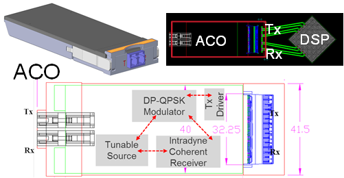
 Karl GassAn ACO module used for optical transport integrates the optics and driver electronics while the accompanying coherent DSP-ASIC residing on the line card.
Systems vendors can thus use their own DSP-ASIC, or a merchant one if they don’t have an in-house design, while choosing the coherent optics from various module makers. The optics and the DSP-ASIC communicate via a high-speed electrical connector on the line card.
ACO design
The OIF completed earlier this year the specification of the CFP2-ACO.
Current CFP2-ACO modules support single-wavelength transmission rates from 100 gigabit to 250 gigabit depending on the baud rate and modulation scheme used. The goal of the CFP8-ACO is to support up to four wavelengths, each capable of up to 400 gigabit-per-second transmissions.
This project is going to drive innovation
“This isn’t something there is a dire need for now but the projection is that this will be needed in two years’ time,” says Karl Gass of Qorvo and the OIF Physical and Link Layer Working Group optical vice chair.
OIF members considered several candidate optical modules for the next-generation ACO before choosing the CFP8. These included the existing CFP2 and the CFP4. There were some proponents for the QSFP but its limited size and power consumption is problematic when considering long-haul applications, says Gass.
 Source: Finisar
One difference between the CFP2 and CFP8 modules is that the electrical connector of the CFP8 supports 16 differential pairs while the CFP2 connector supports 10 pairs.
“Both connectors have similar RF performance and therefore can handle similar baud rates,” says Ian Betty of Ciena and OIF board member and editor of the CFP2-ACO Implementation Agreement. To achieve 400 gigabit on a wavelength for the CFP8-ACO, the electrical connector will need to support 64 gigabaud.
Betty points out that for coherent signalling, four differential pairs per optical carrier are needed. “This is independent of the baud rate and the modulation format,” says Betty.
So while it is not part of the existing Implementation Agreement, the CFP2-ACO could support two optical carriers while the CFP8 will support up to four carriers.
“This is only the electrical connector interface capacity,” says Betty. “It does not imply it is possible to fit this amount of optics and electronics in the size and power budget.” The CFP8 supports a power envelope of 20W compared to 12W of the CFP2.
 The CFP2-ACO showing the optical building blocks and the electrical connector linking the module to the DSP-ASIC. Source: OIF
The CFP8 occupies approximately the same area as the CFP2 but is not as tall such that the module can be doubled-stacked on a line card for a total of 16 CFP8-ACOs on a line card.
Given that the CFP8 will support up to four carriers per module - each up to 400 gigabit - a future line card could support 25.6 terabits of capacity. This is comparable to the total transport capacity of current leading dense WDM optical transport systems.
Rafik Ward, vice president of marketing at Finisar, says such a belly-to-belly configuration of the modules provides future-proofing for next-generation lineside interfaces. “Having said that, it is not clear when, or how, we will be able to technically support a four-carrier coherent solution in a CFP8 form factor,” says Ward.
Oclaro stresses that such a high total capacity implies that sufficient coherent DSP silicon can fit on the line card. Otherwise, the smaller-height CFP8 module may not enable the fully expected card density if the DSP chips are too large or too power-hungry.
OIF goal
Besides resulting in a higher density module, a key OIF goal of the work is to garner as much industry support as possible to back the CFP8-ACO. “How to create the quantity of scale so that deployment becomes less expensive and therefore quicker to implement,” says Gass.
The OIF expects the work to be similar to the development of the CFP2-ACO Implementation Agreement. But one desired difference is to limit the classes associated with the module. The CFP2-ACO has three class categories based on whether the module has a limited and linear output. “The goal of the CFP8-ACO is to limit the designs to single classes per wavelength count,” says Gass.
Gass is looking forward to the CFP8-ACO specification work. Certain standards efforts largely involve making sure components fit into a box whereas the CFP8-ACO will be more engaging. “This project is going to drive innovation and that will drive some technical work,” says Gass.
NeoPhotonics showcases a CFP2-ACO roadmap to 400G
The company demonstrated the CFP2-ACO module transmitting at 100 gigabit using polarisation multiplexed, quadrature phase-shift keying (PM-QPSK) modulation at the recent OFC show. The line-side module is capable of transmitting over 1,000km and also supports PM-16QAM that doubles capacity over metro network distances.
 Ferris LipscombThe CFP2-ACO is a Class 3 design: the control electronics for the modulator and laser reside on the board, alongside the coherent DSP-ASIC chip.
At OFC, NeoPhotonics also demonstrated single-wavelength 400-gigabit transmission using more advanced modulation and a higher symbol rate, and a short-reach 100-gigabit link for inside the data centre using 4-level pulse-amplitude modulation (PAM4) signalling.
Roadmap to 400 gigabit
One benefit of the CFP2-ACO is that the pluggable module can be deployed only when needed. Another is that the optics will work with coherent DSP-ASICs for different systems vendors and merchant chip suppliers.
“After a lot of technology-bragging about the CFP2-ACO, this is the year it is commercial,” says Ferris Lipscomb, vice president of marketing at NeoPhotonics.
Also demonstrated were the components needed for a next-generation CFP2-ACO: NeoPhotonics’ narrow line-width tunable laser and its higher-bandwidth integrated coherent receiver. To achieve 400 gigabit, 32-QAM and a 45 gigabaud symbol rate were used.
Traditional 100-gigabit coherent uses a 32-gigabaud symbol rate. That combined with QPSK and the two polarisations results in a total bit rate of 2 polarisations x 2bits/symbol x 32 gigabaud or 128 gigabits: a 100-gigabit payload and the rest overhead bits. Using 32-QAM instead of QPSK increases the number of bits encoded per symbol from 2 to 5, while increasing the baud rate from 32 to 45 gigabaud adds a speed-up factor of 1.4. Combining the two, the resulting bit rate is 45 gigabaud x 5bits/symbol x 2 polarisations or 450 gigabit overall.
After a lot of technology-bragging about the CFP2-ACO, this is the year it is commercial
Using 32-QAM curtails the transmission distance to 100km due to the denser constellation but such distances are suited for data centre interconnect applications.
“That was the demo [at OFC] but the product is also suitable for metro distances of 500km using 16-QAM and long-haul of 1,000km using 200 gigabit and 8-QAM,” says Lipscomb.
PAM4
The PAM4 demonstration highlighted NeoPhotonics’ laser and receiver technology. The company showcased a single-wavelength link running at 112 gigabits-per-second using its 56Gbaud externally modulated laser (EML) with an integrated driver. The PAM4 link can span 2km in a data centre.
“What is not quite ready for building into modules is the [56Gbaud to 112 gigabit PAM4] DSP, which is expected to be out in the middle to the second half of the year,” says Lipscomb. The company will develop its own PAM4-based optical modules while selling its laser to other module makers.
Lipscomb says four lanes at 56 gigabaud using PAM4 will deliver a cheaper 400-gigabit solution than eight lanes, each at 25 gigabaud.
Silicon Photonics
NeoPhotonics revealed that it is supplying new 1310nm and 1550nm distributed feedback (DFB) lasers to optical module players that are using silicon photonics for their 100-gigabit mid-reach transceivers. These include the 500m PSM-4, and the 2km CWDM4 and CLR4.
Lipscomb says the benefits of its lasers for silicon photonics include their relatively high output power - 40 to 60mW - and the fact that the company also makes laser arrays which are useful for certain silicon photonics applications.
NeoPhotonics’ laser products have been for 100-gigabit modules with reaches of 2km to 10km. “Silicon photonics is usually used for shorter reaches of a few hundred meters,” says Lipscomb. “This new product is our first one aimed at the short reach data centre market segment.”
“Our main products have been for 100-gigabit modules for the longer reaches of 2km to 10km,” says Lipscomb. “Silicon photonics is usually used for shorter reaches of a few hundred meters, and this new [laser] product is our first one aimed at the short reach data centre market segment."
The company says it has multiple customer engagements spanning various wavelength plans and approaches for Nx100-gigabit data centre transceiver designs. Mellanox Technologies is one vendor using silicon photonics that NeoPhotonics is supplying.
OIF document aims to spur line-side innovation
 The CFP2-ACO. Source: OIF
The pluggable CFP2-ACO houses the coherent optics, known as the analogue front end. The components include the tuneable lasers, modulation, coherent receiver, and the associated electronics - the drivers and the trans-impedance amplifier. The Implementation Agreement also includes the CFP2-ACO's high-speed electrical interface connecting the optics to the coherent DSP chip that sits on the line card.
One historical issue involving the design of innovative optical components into systems has been their long development time, says Ian Betty of Ciena, and OIF board member and editor of the CFP2-ACO Implementation Agreement. The lengthy development time made it risky for systems vendors to adopt such components as part of their optical transport designs. Now, with the CFP2-ACO, much of that risk is removed; system vendors can choose from a range of CFP2-ACO suppliers based on the module's performance and price.
Implementation Agreement
Much of the two-year effort developing the Implementation Agreement involved defining the management interface to the optical module. "This is different from our historical management interfaces," says Betty. "This is much more bare metal control of components."
For 7x5-inch and 4x5-inch MSA transponders, the management interface is focused on system-level parameters, whereas for the CFP2-ACO, lower-level optical parameters are accessible given the module's analogue transmission and receive signals.
"A lot of the management is to interrogate information about power levels, or adjusting transfer functions with pre-emphasis, or adjusting drive levels on drivers internal to the device, or asking for information: 'Have you received my RF signal?'," says Betty. "It is very much a lower-level interface because you have separated between the DSP and the optical interface."
The Implementation Agreement's definitions for the CFP2-ACO are also deliberately abstract. The optical technology used is not stated, nor is the module's data rate. "The module has no information associated with the system level - if it is 16-QAM or QPSK [modulation] or what the dispersion is," says Betty.
This is a strength, he says, as it makes the module independent of a data rate and gives it a larger market because any coherent ASIC can make use of this analogue front end. "It lets the optics guys innovate, which is what they are good at," says Betty.
Innovation
The CFP2-ACO is starting to be adopted in a variety of platforms. Arista Networks has added a CFP2-ACO line card to its 7500 data centre switches while several optical transport vendors are using the module for their data centre interconnect platforms.
One obvious way optical designers can innovate is by adding flexible modulation formats to the CFP2-ACO. Coriant's Groove G30 data centre interconnect platform uses CFP2-ACOs that support polarisation-multiplexed, quadrature phase-shift keying (PM-QPSK), polarisation-multiplexed, 8-state quadrature amplitude modulation (PM-8QAM) and PM-16QAM, delivering 100, 150 and 200 gigabit-per-second transmission, respectively. Coriant says the CFP2-ACOs it uses are silicon photonics and indium phosphide based.
Cisco Systems uses CFP2-ACO modules for its first data centre interconnect product, the NCS 1002. The system can use a CFP2-ACO with a higher baud rate to deliver 250 gigabit-per-second using a single carrier and PM-16QAM.
 Ian BettyThe CFP2-ACO enables a much higher density line-side solution than other available form factors. The Groove G30, for example, fits eight such modules on one rack-unit line card. "That is the key enabler that -ACOs give," says Betty.
And being agnostic to a particular DSP, the CFP2-ACO enlarges the total addressable market. Betty hopes that by being able to sell the CFP2-ACO to multiple systems vendors, the line-side optical module players can drive down cost.
Roadmap
Betty says that the CFP2-ACO may offer the best route to greater overall line side capacity rather than moving to a smaller form factor module in future. He points out that in the last decade, the power consumption of the optics has gone down from some 16W to 12W. He does not foresee the power consumption coming down further to the 6W region that would be needed to enable a CFP4-ACO. "The size [of the CFP4] with all the technology available is very doable," says Betty. "But there is not an obvious way to make it [the optics] 6W."
The key issue is the analogue interface which determines what baud rate and what modulation or level of constellation can be put through a module. "The easiest way to lump all that together is with an implementation penalty for the optical front end," says Betty. "If you make the module smaller, you might have a higher implementation penalty, and with this penalty, you might not be able to put a higher constellation through it."
In other words, there are design trade-offs: the data rates supported by the CFP2 modules may achieve a higher overall line-side rate than more, smaller modules, each supporting a lower maximum data rate due to a higher implementation penalty.
"What gets you the ultimate maximum density of data rate through a given volume?" says Betty. "It is not necessarily obvious that making it smaller is better."
Could a CFP2-ACO support 32-QAM and 64-QAM? "The technical answer is what is the implementation penalty of the module?" says Betty. This is something that the industry will answer in time.
"This isn't the same as client optics where there is a spec, you do the spec and there are no brownie points for doing better than the spec, so all you can compete on is cost," says Betty. "Here, you can take your optical innovation and compete on cost, and you can also compete by having lower implementation penalties."
Arista adds coherent CFP2 modules to its 7500 switch
 Martin Hull
Several optical equipment makers have announced ‘stackable’ platforms specifically to link data centres in the last year.
Infinera’s Cloud Xpress was the first while Coriant recently detailed its Groove G30 platform. Arista’s announcement offers data centre managers an alternative to such data centre interconnect platforms by adding dense wavelength-division multiplexing (DWDM) optics directly onto its switch.
For customers investing in an optical solution, they now have an all-in-one alternative to an optical transport chassis or the newer stackable data centre interconnnect products, says Martin Hull, senior director product management at Arista Networks. Insert two such line cards into the 7500 and you have 12 ports of 100 gigabit coherent optics, eliminating the need for the separate optical transport platform, he says.
The larger 11RU 7500 chassis has eight card slots such that the likely maximum number of coherent cards used in one chassis is four or five - 24 or 30 wavelengths - given that 40 or 100 Gigabit Ethernet client-side interfaces are also needed. The 7500 can support up to 96, 100 Gigabit Ethernet (GbE) interfaces.
Arista says the coherent line card meets a variety of customer needs. Large enterprises such as financial companies may want two to four 100 gigabit wavelengths to connect their sites in a metro region. In contrast, cloud providers require a dozen or more wavelengths. “They talk about terabit bandwidth,” says Hull.
With the CFP2-ACO, the DSP is outside the module. That allows us to multi-source the optics
As well as the CFP2-ACO modules, the card also features six coherent DSP-ASICs. The DSPs support 100 gigabit dual-polarisation, quadrature phase-shift keying (DP-QPSK) modulation but do not support the more advanced quadrature amplitude modulation (QAM) schemes that carry more bits per wavelength. The CFP2-ACO line card has a spectral efficiency that enables up to 96 wavelengths across the fibre's C-band.
Did Arista consider using CFP coherent optical modules that support 200 gigabit, and even 300 and 400 gigabit line rates using 8- and 16-QAM? “With the CFP2-ACO, the DSP is outside the module,” says Hull. “That allows us to multi-source the optics.”
The line card also includes 256-bit MACsec encryption. “Enterprises and cloud providers would love to encrypt everything - it is a requirement,” says Hull. “The problem is getting hold of 100-gigabit encryptors.” The MACsec silicon encrypts each packet sent, avoiding having to use a separate encryption platform.
CFP4-ACO and COBO
As for denser CFP4-ACO coherent modules, the next development after the CFP2-ACO, Hull says it is still too early, as it is with for 400 gigabit on-board optics being developed by COBO and which is also intended to support coherent. “There is a lot of potential but it is still very early for COBO,” he says.
“Where we are today, we think we are on the cutting edge of what can be delivered on a line card,” says Hull. “Getting everything onto that line card is an engineering achievement.”
Future developments
Arista does not make its own custom ASICs or develop optics for its switch platforms. Instead, the company uses merchant switch silicon from the likes of Broadcom and Intel.
According to Hull, such merchant silicon continues to improve, adding capabilities to Arista’s top-of-rack ‘leaf’ switches and its more powerful ‘spine’ switches such as the 7500. This allows the company to make denser, higher-performance platforms that also scale when coupled with software and networking protocol developments.
Arista claims many of the roles performed by traditional routers can now be fulfilled by the 7500 such as peering, the exchange of large routing table information between routers using the Border Gateway Protocol (BGP). “[With the 7500], we can have that peering session; we can exchange a full set of routes with that other device,” says Hull.
"We think we are on the cutting edge of what can be delivered on a line card”
The company uses what it calls selective route download where the long list of routes is filtered such that the switch hardware is only programmed with the routes to be communicated with. Hull cites as an example a content delivery site that sends content to subscribers. The subscribers are typically confined to a known geographic region. “I don’t need to have every single Internet route in my hardware, I just need the routes to reach that state or metro region,” says Hull.
By having merchant silicon that supports large routing tables coupled with software such as selective route download, customers can use a switch to do the router’s job, he says.
Arista says that in 2016 and 2017 it will continue to introduce leaf and spine switches that enable data centre customers to further scale their networks. In September Arista launched Broadcom Tomahawk-based switches that enable the transition from 10 gigabit server interfaces to 25 gigabit and the transition from 40 to 100 gigabit uplinks.
Longer term, there will be 50 GbE and iterations of 400 and one terabit Ethernet, says Hull. And all this relates to the switch silicon. At present 3.2 terabit switch chips are common and already there is a roadmap to 6.4 and even 12.8 terabits by increasing both the chip’s pin count and using PAM-4 alongside the 25 gigabit signalling to double input/ output again. A 12.8 terabit switch may be a single chip, says Hull, or it could be multiple 3.2 terabit building blocks integrated together.
“It is not just a case of more ports on a box,” says Hull. “The boxes have to be more capable from a hardware perspective so that the software can harness that.”
COBO looks inside and beyond the data centre
The Consortium of On-Board Optics is working on 400 gigabit optics for the data centre and also for longer-distance links. COBO is a Microsoft-led initiative tasked with standardising a form factor for embedded optics.
Established in March 2015, the consortium already has over 50 members and expects to have early specifications next year and first hardware by late 2017.
 Brad Booth
Brad Booth, the chair of COBO and principal architect for Microsoft’s Azure Global Networking Services, says Microsoft plans to deploy 100 gigabit in its data centres next year and that when the company started looking at 400 gigabit, it became concerned about the size of the proposed pluggable modules, and the interface speeds needed between the switch silicon and the pluggable module.
“What jumped out at us is that we might be running into an issue here,” says Booth.
This led Microsoft to create the COBO industry consortium to look at moving optics onto the line card and away from the equipment’s face plate. Such embedded designs are already being used for high-performance computing, says Booth, while data centre switch vendors have done development work using the technology.
On-board optics delivers higher interface densities, and in many cases in the data centre, a pluggable module isn’t required. “We generally know the type of interconnect we are using, it is pretty structured,” says Booth. But the issue with on-board optics is that existing designs are proprietary; no standardised form factor exists.
“It occurred to us that maybe this is the problem that needs to be solved to create better equipment,” says Booth. Can the power consumed between switch silicon and the module be reduced? And can the interface be simplified by eliminating components such as re-timers?
“This is worth doing if you believe that in the long run - not the next five years, but maybe ten years out - optics needs to be really close to the chip, or potentially on-chip,” says Booth.
400 gigabit
COBO sees 400 gigabit as a crunch point. For 100 gigabit interconnect, the market is already well served by various standards and multi-source agreements so it makes no sense for COBO to go head-to-head here. But should COBO prove successful at 400 gigabit, Booth envisages the specification also being used for 100, 50, 25 and even 10 gigabit links, as well as future speeds beyond 400 gigabit.
The consortium is developing standardised footprints for the on-board optics. “If I want to deploy 100 gigabit, that footprint will be common no matter what the reach you are achieving with it,” says Booth. “And if I want a 400 gigabit module, it may be a slightly larger footprint because it has more pins but all the 400 gigabit modules would have a similar footprint.”
COBO plans to use existing interfaces defined by the industry. “We are also looking at other IEEE standards for optical interfaces and various multi-source agreements as necessary,” says Booth. COBO is also technology agnostic; companies will decide which technologies they use to implement the embedded optics for the different speeds and reaches.
“This is worth doing if you believe that in the long run - not the next five years, but maybe ten years out - optics needs to be really close to the chip, or potentially on-chip."
Reliability
Another issue the consortium is focussing on the reliability of on-board optics and whether to use socketed optics or solder the module onto the board. This is an important consideration given that is it is the vendor’s responsibility to fix or replace a card should a module fail.
This has led COBO to analyse the causes of module failure. Largely, it is not the optics but the connections that are the cause. It can be poor alignment with the electrical connector or the cleanliness of the optical connection, whether a pigtail or the connectors linking the embedded module to the face plate. “The discussions are getting to the point where the system reliability is at a level that you have with pluggables, if not better,” says Booth.
Dropping below $1-per-gigabit
COBO expects the cost of its optical interconnect to go below the $1-per-gigabit industry target. “The group will focus on 400 gigabit with the perception that the module could be four modules on 100 gigabit in the same footprint,” says Booth. Using four 100 gigabit optics in one module saves on packaging and the printed circuit board traces needed.
Booth says that 100 gigabit optics is currently priced between $2 and $3-per-gigabit. “If I integrate that into a 400 gigabit module, the price-per-gig comes down significantly” says Booth. “All the stuff I had to replicate four times suddenly is integrated into one, cutting costs significantly in a number of areas.” Significantly enough to dip below the $1-per-gigabit, he says.
Power consumption and line-side optics
COBO has not specified power targets for the embedded optics in part because it has greater control of the thermal environment compared to a pluggable module where the optics is encased in a cage. “By working in the vertical dimension, we can get creative in how we build the heatsink,” says Booth. “We can use the same footprint no matter whether it is 100 gigabit inside or 100 gigabit outside the data centre, the only difference is I’ve got different thermal classifications, a different way to dissipate that power.”
The consortium is investigating whether its embedded optics can support 100 gigabit long-haul optics, given such optics has traditionally been implemented as an embedded design. “Bringing COBO back to that market is extremely powerful because you can better manage the thermal environment,” says Booth. And by removing the power-hungry modules away from the face plate, surface area is freed up that can be used for venting and improving air flow.
“We should be considering everything is possible, although we may not write the specification on Day One,” says Booth. “I’m hoping we may eventually be able to place coherent devices right next to the COBO module or potentially the optics and the coherent device built together.
“If you look at the hyper-scale data centre players, we have guys that focus just as much on inside the data centre as they do on how to connect the data centres in within a metro area, national area and then sub-sea,” says Booth. “That is having an impact because when we start looking at what we want to do with those networks, we want to have some level of control on what we are doing there and on the cost.
“We buy gazillions of optical modules for inside the data centre. Why is it that we have to pay exorbitant prices for the ones that we are not using inside [the data centre],” he says.
“I can’t help paint a more rosier picture because when you have got 1.4 million servers, if I end up with optics down to all of those, that is a lot of interconnect“
Market opportunities
Having a common form factor for on-board optics will allow vendors to focus on what they do best: the optics. “We are buying you for the optics, we are not buying you for the footprint you have on the board,” he says.
Booth is sensitive to the reservations of optical component makers to such internet business-led initiatives. “It is a very tough for these guys to extend themselves to do this type of work because they are putting a lot of their own IP on the line,” says Booth. “This is a very competitive space.”
But he stresses it is also fiercely competitive between the large internet businesses building data centres. “Let’s sit down and figure out what does it take to progress this industry. What does it take to make optics go everywhere?”
Booth also stresses the promising market opportunities COBO can serve such as server interconnect.
“When I look at this market, we are talking about doing optics down to our servers,” says Booth. “I can’t help paint a more rosier picture because when you have got 1.4 million servers, if I end up with optics down to all of those, that is a lot of interconnect.“
Micro QSFP module to boost equipment port densities
 Nathan Tracy
The μQSFP will support both copper and optical cabling, and will have an improved thermal performance, benefitting interfaces and platforms.
“There is always a quest for greater port density or aggregate bandwidth,” says Nathan Tracy, technologist at TE Connectivity and chair of the μQSFP MSA.
The challenge for the module makers is to provide denser form factors to increase overall system traffic. “As we go to higher densities, we are also increasing the thermal load,” says Tracy. “And so now it is a mechanical and a thermal [design] problem, and both need to be solved jointly.”
The thermal load is increased since the μQSFP supports interfaces that consume up to 3.5 W - like the QSFP - while having the width of the smaller SFP rated at 1.5 W.
“We are limited in the directions we can pull the heat out,” says Tracy. “If we are going to enable a higher density form factor that has the same width as an SFP but it is going to have the functionality of a QSFP, now we have a problem.”
This requires the MSA engineers to develop new ways to rid the μQSFP of its heat.
If we are going to enable a higher density form factor that has the same width as an SFP but it is going to have the functionality of a QSFP, now we have a problem
Heat transfer and other challenges
The volume and surface area of a module determine the overall thermal capacity or thermal density. The module can be modelled as an electrical circuit, with heat flow equivalent to current, while each interface has a thermal resistance.
There are three interfaces - thermal resistances - associated with a module: between the heat source and the module case, the case and the heat sink, and the heat sink and ambient air. These three thermal resistances are in series and the goal is to reduce them to ensure greater heat flow.
The module’s circuitry generates heat and the interface between the circuitry and the module’s case is one of the thermal resistances. “You are going to have a heat source in the module and no matter what you do, there is going to be some thermal resistance from that source to the module housing,” says Tracy.
You have to get good signal integrity through that electrical interface because we are working at 25 gigabit-per-second (Gbps) data rates today and we know 50 Gbps data rates are coming
The second thermal resistance - one that the µQSFP eliminates - is between the module housing and the heat sink. Sliding a module into its cage puts it into contact with the heat sink. But the contact between the two surfaces is imperfect, making heat extraction harder. Building the heat sink into the μQSFP module avoids using the sliding design.
The remaining thermal resistance is between the heat sink and the cooling air blown through the equipment. This thermal resistance between the heat sink's metal fin structure and the air flow exists however good the heat sink design, says Tracy.
Other design challenges include achieving signal integrity when cramming the four electrical lanes across the µQSFP’s smaller width, especially when its support 25 Gbit/s lanes and likely 50 Gbit/s in future, says Tracy.
And the module's optical interface must also support duplex LC and MPO connectors to interoperate with existing cabling.
“It is all a balancing act,” says Tracy.
Applications
The μQSFP is aimed at platforms such as 4.8 and 6.4 Tbps capacity switches. The QSFP is used for current 3.2 Tbps platforms but greater port densities will be needed for these next-generation platforms. The size of the μQSFP means 48 ports will fit in the space 36 QSFPs currently occupy, while 72 μQSFPs will fit on a line card if three rows are used.
The μQSFP may also find use outside the data centre for longer, 100 km reaches. “Today you can buy SFP modules that go 100 km,” says Tracy. “With this form factor, we are creating the capability to go up to four lanes in the same width as an SFP and, at the same time, we are improving the thermal performance significantly over what an SFP can do.”
The Micro QSFP group is not saying when the µQSFP MSA will be done. But Tracy believes the μQSFP would be in demand were it available now. Its attraction is not just the greater port density, but how the µQSFP would aid systems engineers in tackling their thermal design challenges.
The pluggable form factor will allow air to flow from the face plate and through the module to where ICs and other circuitry reside. Moreover, since 32 μQSFP ports will take up less face-plate area than 32 QSFPs, perforations could be added, further improving airflow.
“If you look at the QSFP or SFP, it does not allow airflow through the cage from the front [plate] to the back,” says Tracy.
The μQSFP MSA founding members are Avago Technologies, Broadcom, Brocade, Cisco, Dell, Huawei, Intel, Lumentum (formerly JDSU), Juniper Networks, Microsoft, Molex, and TE Connectivity.
Altera unveils its optical FPGA prototype
Altera has been showcasing a field-programmable gate array (FPGA) chip with optical interfaces. The 'optical FPGA' prototype makes use of parallel optical interfaces from Avago Technologies.
Combining the FPGA with optics extends the reach of the chip's transceivers to up to 100m. Such a device, once commercially available, will be used to connect high-speed electronics on a line card without requiring exotic printed circuit board (PCB) materials. An optical FPGA will also be used to link equipment such as Ethernet switches in the data centre.
"It is solving a problem the industry is going to face," says Craig Davis, product marketing manager at Altera. "As you go to faster bit-rate transceivers, the losses on the PCB become huge."
What has been done
Altera's optical FPGA technology demonstrator combines a large FPGA - a Stratix IV EP4S100G5 - to two Avago 'MicroPod' 12x10.3 Gigabit-per-second (Gbps) optical engines.
 Avago's MicroPod 12x10Gbps optical engine deviceThe FPGA used has 28, 11.3Gbps electrical transceivers and in the optical FPGA implementation, 12 of the interfaces connect to the two MicroPods, a transmitter optical sub-assembly (TOSA) and a receiver optical sub-assembly (ROSA).
The MicroPod measures 8x8mm and uses 850nm VCSELs. The two optical engines interface to a MTP connector and consume 2-3W. Each MicroPod sits in a housing - a land grid array compression socket - that is integrated as part of the FPGA package.
"The reason we are doing it [the demonstrator] with a 10 Gig FPGA and 10 Gig transceivers is that they are known, good technologies," says Davis. "It is a production GT part and known Avago optics."
Why it matters
FPGAs, with their huge digital logic resources and multiple high-speed electrical interfaces, are playing an increasingly important role in telecom and datacom equipment as the cost to develop application-specific standard product (ASSP) devices continues to rise.
The 40nm-CMOS Stratix IV FPGA family have up to 32, 11.3Gbps transceivers, while Altera's latest 28nm Stratix V FPGAs support up to 66x14.1Gbps transceivers, or 4x28Gbps and 32x12.5Gbps electrical transceivers on-chip.
Altera's FPGAs can implement the 10GBASE-KR backplane standard at spans of up to 40 inches. "You have got the distances on the line card, the two end connectors and whatever the distances are across a 19-inch rack," says Davis. Moving to 28Gbps transceivers, the distance is reduced significantly to several inches only. To counter such losses expensive PCBs must be used.
One way to solve this problem is to go optical, says Davis. Adding 12-channel 10Gbps optical engines means that the reach of the FPGAs is up to 100m, simplifying PCB design and reducing cost while enabling racks and systems to be linked.
 The multimode fibre connector to the MicroPod
Developing an optical FPGA prototype highlights that chip vendors already recognise the role optical interfaces will play.
It is also good news for optical component players as the chip market promises a future with orders of magnitude greater volumes than the traditional telecom market.
The optical FPGA is one target market for silicon photonics players. One, Luxtera, has already demonstrated its technology operating at 28Gbps.
What next
Altera stresses that this is a technology demonstrator only.
The company has not made any announcements regarding when its first optical FPGA product will be launched, and whether the optical technology will enter the market interfacing to its FPGAs' 11.3Gbps, 14.1Gbps or highest-speed 28Gbps transceivers.
 The undersideof the FPGA, showing the 1,932-pin ball grid array