
Xilinx unveils a new class of compute IC
Programmable device company Xilinx has outlined an architecture that it claims represents a new class of computing chip.
The silicon architecture has been four years in the making, involved 1,500 engineers and cost over $1 billion in R&D investment.
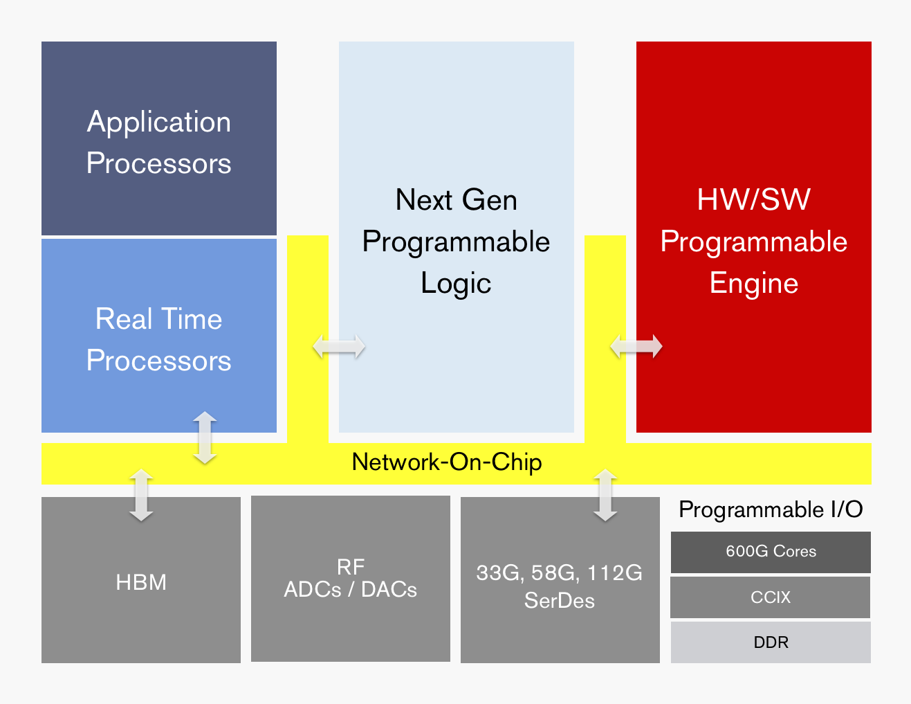 ACAP's functional blocks. Source: Xilinx
Dubbed the adaptive compute acceleration platform (ACAP), the first device will be fabricated using TSMC’s state-of-the-art 7nm CMOS process and will tape out later this year. The largest ACAP devices will use as many as 50 billion transistors.
“Based on the limited information from Xilinx, it is difficult to say what ACAP is, much less whether it creates a new product category,” says Linley Gwennap, principal analyst at The Linley Group.
That said, Gwennap believes the next-generation Xilinx products are far more than simply moving its FPGA technology to a 7nm CMOS. “The company has clearly put significant effort into improving the capabilities of these products to address 5G wireless, machine learning (AI), and other advanced applications,” says Gwennap.
The largest ACAP devices will use as many as 50 billion transistors
Trends
Xilinx says the relentless growth in data coupled with the emergence of artificial intelligence (AI) is driving new computing requirements. At the same time, Moore’s law is slowing down while the speed of innovation is outpacing silicon development cycles.
Victor Peng, Xilinx’s CEO, stresses that while AI is still in its infancy, the technology will be adopted across multiple industries. Thousands of applications will integrate some form of intelligence and this will occur at the network edge and in the cloud. “You will see AI end-to-end,” says Peng.
 Victor Peng
In this new era, chip architectures will be heterogeneous and use processing accelerators. “If you are going to have an intelligent, connected world, it really needs to be adaptable,” says Peng. “It needs to be adaptable because you cannot predict all the needs of the future.”
Gwennap says many companies have already delivered heterogenous chips, given the term heterogeneous refers to a mix of CPU, graphics processor unit (GPU) and digital signal processor (DSP) cores. “This includes every smartphone and PC processor shipping today,” he says.
It also is not clear what ‘adaptive’ means, adds Gwennap: “But if you interpret it to mean FPGA, then both Xilinx and Altera (now Intel) have delivered chips mixing CPUs, DSPs, and FPGAs for years.”
It configures a processor to do a job then, pffft, it has gone
ACAP
Xilinx is not yet detailing the ACAP architecture until the first devices are launched but it has listed the main architectural features.
“Overall, it can be programmed at the hardware level and it has enough architectural features that it can be programmed purely from a software perspective,” says Peng. This means that things can be changed not just at the software level but down at the hardware level, dynamically, while the device is running.
“It configures a processor to do a job then, pffft, it has gone,” says David Manners, the veteran chip journalist at Electronics Weekly who has been covering Xilinx since it was founded in the 1980s.
The ACAP architecture will include both application and real-time processors as well as programmable logic for digital signal processing (DSP) and a hierarchy of distributed memory. The chip will also feature a high-speed network-on-a-chip linking the functional blocks and arbitrating between them.
ACAP will support various generations of DDR memory and certain family devices will include high-bandwidth 3D stacked memory. There will also be device members that use RF analogue-to-digital and digital-to-analogue converters.
In turn, ACAP will have fast input-output circuitry with serial/deserialisers (SERDES) running at 33, 58 and even 112 gigabit-per-second (Gbps) rates. Xilinx demonstrated its latest 112Gbps serdes at the recent OFC show held in San Diego.
Certain ACAP devices will use a novel engine that is software and hardware programmable. Programming the engine at the software level will require some embedded expertise.
“We are always looking at how we can use our hardware programming expertise to get another level of optimisation beyond just software-programmable blocks,” says Peng. Xilinx will detail the engine’s workings later this year.
Xilinx says the 7nm ACAP will deliver a 20x AI compute performance improvement and 4x the 5G communications bandwidth compared to its current 16nm FPGAs.
The company has already delivered software tools for ACAP to select customers and expects first device shipments in 2019.
Data-centre focus
Peng, who has been CEO since January, says the data centre market is now Xilinx’s top priority segment.
Data centres require ever more computing while their networked architectures continue to evolve. This represents an attractive market for Xilinx especially given its programmable devices not only serve computing but also storage and networking requirements.
Xilinx has also been expanding its software development environments that let its devices be programmed at a higher level by developers that have little or no knowledge of the underlying hardware. This contrasts with traditional Xilinx FPGA users that by nature are hardware engineers. “There are easily 1000x more software developers than FPGA developers,” says Peng.
Companies such as Amazon, Alibaba, Huawei, Baidu, Nimbix and Tencent also offer FPGAs-as-a-service as part of their cloud offerings.
The central role of software in data centres may have caused chips to recede into the background, yet Xilinx will argue that the nature of the silicon has never been more important.
Infinera’s ICE flow
Infinera’s newest Infinite Capacity Engine 5 (ICE5) doubles capacity to 2.4 terabits. The ICE, which comprises a coherent DSP and a photonic integrated circuit (PIC), is being demonstrated this week at the OFC show being held in San Diego.
Infinera has also detailed its ICE6, being developed in tandem with the ICE5. The two designs represent a fork in Infinera’s coherent engine roadmap in terms of the end markets they will address.
 Geoff BennettThe ICE5 is targeted at data centre interconnect and applications where fibre in being added towards the network edge. The next-generation access network of cable operators is one such example. Another is mobile operators deploying fibre in preparation for 5G.
First platforms using the ICE5 will be unveiled later this year and will ship early next year.
Infinera’s ICE6 is set to appear two years after the ICE5. Like the ICE4, Infinera’s current Infinite Capacity Engine, the ICE6 will be used across all of Infinera’s product portfolio.
Meanwhile, the 1.2 terabit ICE4 will now be extended to work in the L-band of optical wavelengths alongside the existing C-band, effectively doubling a fibre’s capacity available for service providers.
Infinera’s decision to develop two generations of coherent designs follows the delay in bringing the ICE4 to market.
“The fundamental truth about the industry today is that coherent algorithms are really hard,” says Geoff Bennett, director, solutions and technology at Infinera.
By designing two generations in parallel, Infinera seeks to speed up the introduction of its coherent engines. “With ICE5 and ICE6, we have learnt our lesson,” says Bennett. “We recognise that there is an increased cadence demanded by certain parts of the industry, predominately the internet content providers.”
ICE5
The ICE5 uses a four-wavelength indium-phosphide PIC that, combined with the FlexCoherent DSP, supports a maximum symbol rate of 66Gbaud and a modulation rate of up to 64-ary quadrature amplitude modulation (64-QAM).
Infinera says that the FlexCoherent DSP used for ICE5 is a co-development but is not naming its partners.
Using 64-QAM and 66Gbaud enables 600-gigabit wavelengths for a total PIC capacity of 2.4 terabits. Each PIC is also ‘sliceable’, allowing each of the four wavelengths to be sent to a different location.
Infinera is not detailing the ICE5’s rates but says the design will support lower rates, as low as 200 gigabit-per-second (Gbps) or possibly 100Gbps per wavelength.
Bennett highlights 400Gbps as one speed of market interest. Infinera believes its ICE5 design will deliver 400 gigabits over 1,300km. The 600Gbps wavelength implemented using 64-QAM and 66Gbaud will have a relatively short reach of 200-250km.
“A six hundred gigabit wavelength is going to be very short haul but is ideal for data centre interconnect,” says Bennett, who points out that the extended reach of 400-gigabit wavelengths is attractive and will align with the market emergence of 400 Gigabit Ethernet client signals.
Probabilistic shaping squeezes the last bits of capacity-reach out of the spectrum
Hybrid Modulation
The 400-gigabit will be implemented using a hybrid modulation scheme. While Infinera is not detailing the particular scheme, Bennett cites several ways hybrid modulation can be implemented.
One hybrid modulation technique is to use a different modulation scheme on each of the two light polarisations as a way of offsetting non-linearities. The two modulation schemes can be repeatedly switched between the two polarisation arms. “It turns out that the non-linear penalty takes time to build up,” says Bennett.
Another approach is using blocks of symbols, varying the modulation used for each block. “The coherent receiver has to know how many symbols you are going to send with 64-QAM and how many with 32-QAM, for example,” he says
A third hybrid modulation approach is to use sub-carriers. In a traditional coherent system, a carrier is the output of the transmit laser. To generate sub-carriers, the coherent DSP’s digital-to-analogue converter (DAC) applies a signal to the modulator which causes the carrier to split into multiple sub-carriers.
To transmit at 32Gbaud, four sub-carriers can be used, each modulated at 8Gbaud, says Bennett. Nyquist shaping is used to pack the sub-carriers to ensure there is no spectral efficiency penalty.
“You now have four parallel streams and you can deal with them independently,” says Bennett, who points out that 8Gbaud turns out to be an optimal rate in terms of minimising non-linearities made up of cross-phase and self-phase modulation components.
Sub-carriers can be described as a hybrid modulation approach in that each sub-carrier can be operated at a different baud rate and use a different modulation scheme. This is how probabilistic constellation shaping - a technique that improves spectral efficiency and which allows the data rate used on a carrier to be fine-tuned - will be used with the ICE6, says Infinera.
For the ICE5, sub-carriers are not included. “For the applications we will be using ICE5 for, the sub-carrier technology is not as important,” says Bennett. “Where it is really important is in areas such as sub-sea.”
Silicon photonics has a lower carrier mobility. It is going to be harder and harder to build such parts of the optics in silicon.
Probabilistic constellation shaping
Infinera is not detailing the longer-term ICE6 beyond highlights two papers that were presented at the ECOC show last September that involved a working 100Gbaud sub-carrier-driven wavelength and probabilistic shaping applied to a 1024-QAM signal.
The 100Gbaud rate will enable higher capacity transponders while the use of probabilistic shaping will enable greater spectral efficiency. “Probabilistic shaping squeezes the last bits of capacity-reach out of the spectrum,” says Bennett.
“In ICE6 we will be doing different modulation on each sub-carrier,” says Bennett. “That will be part of probabilistic constellation shaping.” And assuming Infinera adheres to 8Gbaud sub-carriers, 16 will be used for a 100Gbaud symbol rate.
Infinera argues that the interface between the optics and the DSP becomes key at such high baud rates and it argues that its ability to develop both components will give it a system design advantage.
The company also argues that its use of indium phosphide for its PICs will be a crucial advantage at such high baud rates when compared to silicon photonics-based solutions. “Silicon photonics has a lower carrier mobility,” says Bennett. “It is going to be harder and harder to build such parts of the optics in silicon.”
ICE4 embraces the L-band
Infinera’s 1.2 terabit six-wavelength ICE4 was the first design to use Nyquist sub-carriers and SD-FEC gain sharing, part of what Infinera calls its advanced coherent toolkit.
At OFC, Infinera announced that the ICE4 will add the L-band in addition to the C-band. It also announced that the ICE4 has now been adopted across Infinera’s platform portfolio.
The first platforms to use the ICE4 were the Cloud Xpress 2, the compact modular platform used for data centre interconnect, and the XT-3300, a 1 rack-unit (1RU) modular platform targeted at long-haul applications.
A variant of the platform tailored for submarine applications, the XTS-3300, achieved a submarine reach of 10,500km in a trial last year. The modulation format used was 8-QAM coupled with SD-FEC gain-sharing and Nyquist sub-carriers. The resulting spectral efficiency achieved was 4.5bits/s/Hz. In comparison, standard 100-gigabit coherent transmission has a spectral efficiency of 2bits/s/Hz. The total capacity supported in the trial was 18.2 terabits.
Since then, the ICE4 has been added the various DTN-X chassis including the XT-3600 2.4 terabit 4RU platform.
Rockley Photonics showcases its in-packaged design at OFC
The packaged design includes Rockley's own 2 billion transistor layer 3 router chip, and its silicon photonics-based optical transceivers. The layer 3 router chip, described as a terabit device, also includes mixed-signal circuits needed for the optical transceevers' transmit and receive paths.
 Source: Rockley Photonics (annotated by Gazettabyte).
Rockley says it is using 500m-reach PSM4 transceivers for the design and that while a dozen ribbon cables are shown, this does not mean there are 12 100-gigabit PSM4 transceivers. The company is not saying what the total optical input-output is.
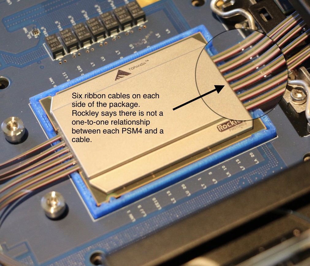 Source: Rockley Photonics (annotated by Gazettabyte).
The company has said it is not looking to enter the marketplace as a switch chip player competing with the likes of Broadcom, Intel, Cavium, Barefoot Networks and Innovium. To develop such a device and remain competitive requires considerable investment and that is not Rockley's focus. Instead, it is using its router chip as a demonstrator to show the marketplace what can be done and that the technology works.
When asked what progress Rockley is making showcasing its technology, its CEO Andrew Rickman said: “It is going very well but nothing we can say publicly."
The switch chip makers continue to use electrical interfaces for their state-of-the-art switches which have a capacity of 12.8 terabits. It still remains to be seen which generation of switch chip will finally adopt in-packaged optics and whether on-board optics designs such as COBO will be adopted first.
For the full interview with CEO Andrew Rickman, click here.
DustPhotonics reveals its optical transceiver play
A start-up that has been active for a year has dropped its state of secrecy to reveal it is already shipping its first optical transceiver product.
The company, DustPhotonics, is backed by private investors and recently received an undisclosed round of funding that will secure the company’s future for the next two years.
Product plans
DustPhotonics' first product is the multi-mode 100m-reach 100GBASE-SR4 QSFP28. The company will launch its first 400-gigabit optical modules later this year.
 Ben Rubovitch
“We probably are going to be one of the first to market with [400-gigabit] QSFP-DD and OSFP multi-mode solutions,” says Ben Rubovitch, CEO of DustPhotonics.
The start-up has developed 50 gigabit-per-lane technology required for higher-speed modules such as the QSFP56, QSFP-DD and OSPF pluggables. The QSFP-DD form factor is designed to be backwards compatible with the QSFP and QSFP28 and is backed by the likes of Facebook and Cisco, while the OSFP is a new form factor supported by Google and switch maker Arista Networks.
DustPhotonics chose the 4-lane 25-gigabit QSFP28 to prove the working of its 50 gigabit-per-lane technology. “The reason we did that is that the PAM-4 chipsets weren’t ready when we started,” says Rubovitch. “So we invested the first year solving the production issues and the optical interface and used the QSFP28 as the platform.”
The challenge with a 50 gigabit-per-lane optical interface is that the photo-detector aperture used is smaller. “So on our QSFP28 we used a small photo-detector to prove the optical solution,” says Rubovitch.
The start-up is now developing faster speed multi-mode designs: a 200-gigabit QSFP56 pluggable, a 400-gigabit QSFP-DD implementing the 400GBASE-SR8 standard and a similar active optical cable variant; products that it hopes to sample in the second quarter of this year. This will be followed by similar SR8 implementations using the OSFP.
 DustPhotonics' optical product roadmap. Source: Gazettabyte/ DustPhotonics.
DustPhotonics is also adapting its optical packaging technology to support single-mode designs: the 500m IEEE 400GBASE-DR4 and the 2km 400G-FR4, part of the 100G Lambda multi-source agreement (MSA). Both the DR4 and FR4 designs use 100-gigabit optical lanes.
Technology
Rubovitch says that despite the many optical transceiver players and the large volumes of modules now manufactured, pluggable optics remain expensive. “The front panel of a top-of-rack switch [populated with modules] costs ten times more than the switch itself,” he says.
DustPhotonics has tackled the issue of cost by simplifying the module’s bill of materials and the overall manufacturing process.
The start-up buys the lasers and electronic ICs needed and adds its own free-space optics for both multi-mode and single-mode transceiver designs. “It is all plastic-molded so we don’t use any glass types or any integrated lasers and that simplifies much of the process,” says Rubovitch. Indeed, he claims the design reduces the bill of materials of its transceivers by between 30 and 50 percent.
The front panel of a top-of-rack switch [populated with modules] costs ten times more than the switch itself
DustPhotonics has also developed a passive alignment process. “We have narrowed the one accurate step - where we align the optics - to one machine,” says Rubovitch. “This compares to two steps ‘accurate’ and one step ‘align’ for active alignment.” Active alignment for a QSFP28 module takes ten minutes, he says, whereas DustPhotonics’ passive alignment process takes under a minute per module.
“There is also a previous manufacturing stage where we place the VCSELs and photo-detectors on a substrate itself and we don’t need accuracy here, unlike other solutions,” he says.
The overall result is a simpler, more cost-effective design. “We are already manufacturing in a volume production line and we see the numbers and how competitive we are, and it is going to create an even larger advantage at 400 gigabits,” says Rubovitch.
DustPhotonics’ passive alignment process takes under a minute per module
What next?
DustPhotonics is also developing embedded optics, where the optics are placed next to an ASIC, and even in-package designs where the optics and ICs are co-packaged.
Rubovitch says such technologies will be needed because of the very high power 100-gigabit electrical transceivers consume on a switch chip, for example, as well the silicon area they require; precious silicon real estate needed to cope with the ever-increasing packet-processing demands. “Bringing the optics very close [to the chip] can help solve those issues for the switch providers,” he says.
As Rockley Photonics’ CEO, Andrew Rickman, observed recently, combining optics with the switch silicon has long been discussed yet has still to be embraced by the switch chip makers. This explains why Rockley developed its own switch ASIC to demonstrate a complete in-packaged reference design.
Rubovitch agrees that the concept of optics replacing electrical interfaces has long been spoken of but that hasn’t happened due to copper speeds continuing to advance. There is already a 100 gigabit-per-lane solution that will meet the demands of the next generation of switch designs, he says: “It really depends on what is going to be the next leap: 200 gigabits or 400-gigabits.”
Using optics to replace electrical interfaces could come with the advent of 25 terabit switch silicon or maybe the generation after. “Or maybe something in between: 25 terabit solutions will start to move gradually to a more packaged solution or at least closer on-board optics,” concludes Rubovitch.
Lumentum jolts the industry with Oclaro acquisition
Lumentum announced on Monday its plan to acquire Oclaro in a deal worth $1.8 billion.
The prospect of consolidation among optical component players has long been mooted yet the announcement provided the first big news jolt at the OFC show, being held in San Diego this week.
 Alan Lowe“Combined, we will be an industry leader in telecom transmission and transport as well as 3D sensing,” said Alan Lowe, president and CEO of Lumentum, on an analyst call discussing the deal.
Lumentum says their joint revenues totalled $1.7 billion with a 39% gross margin over the last year. And $60 million in synergies are forecast in the second year after the deal closes, which is expected to happen later this year.
The $1.8 billion acquisition will comprise 56 percent cash and 44 percent Lumentum stock. Lumentum will also raise $550 million to help finance the deal.
“This is a big deal as it consolidates the telecom part of the component market,” says Daryl Inniss, business development manager at OFS Fitel and former market research analyst.
Background
Lowe said that ever since Lumentum became a standalone company three years ago, the firm concentrated on addressing the increase in optical communications demand that started in late 2015 and then last year on ramping the production of its 3D sensing components. “Execution on major M&As had to wait,” he said.
The company investigated potential acquisitions and evaluated several key technologies including silicon photonics and indium phosphide. This led to it alighting on Oclaro with its indium phosphide and photonic integrated circuit (PIC) expertise.
Lowe also highlighted Oclaro’s strategy of the last five years of first trimming its business lines and then successfully executing on delivering optical transmission products.
Oclaro’s CEO, Greg Dougherty, CEO of Oclaro, described how his company has focussed on delivering differentiated photonic chip products to various growing end markets. “This is a very good combination for both companies and for the industry,” said Dougherty.
There is no overabundance in [optical] chip designers worldwide and together we have the strongest chip designer team in the world
Business plans
Lumentum’s business includes telecom transport components, modules and sub-systems. Its products include reconfigurable optical add/drop multiplexers (ROADMs), pump lasers, optical amplifiers and submarine products. In the second half of 2017, Lumentum’s telecom revenue mix was split three quarters telecom transport with transmission products accounted for the remaining quarter. Other Lumentum businesses include industrial lasers and 3D sensing.
In contrast, Oclaro’s focus in solely transmission components and modules, with the revenue mix in its most recent quarter being 53 percent telecom line side and 47 percent datacom client-side products.
The combined R&D resources of the merged company will allow it to do a much better job at supporting datacom products using the new QSFP-DD and OSFP form factors. “Right now I’m guessing that Alan is spread thin and I know the Oclaro datacom team has been spread thin,” says Dougherty.
The acquisition will also pool the two companies’ fabrication facilities.
Lumentum has already moved its lithium niobate manufacturing to its main gallium arsenide and indium phosphide fab in San Jose, California. San Jose also hosts a separate planar lightwave circuit fab.
Oclaro, which is headquartered in San Jose, has three photonic chip fabrication sites: an indium phosphide laser fab for datacom in Japan that makes directly modulated lasers (DMLs) and electro-absorption modulated lasers (EMLs), an indium phosphide fab in the UK that manufactures coherent optical components and sub-assemblies, and a lithium niobate fab in Italy.
The acquisition will also bolster the company’s chip design resources. “There is no overabundance in [optical] chip designers worldwide and together we have the strongest chip designer team in the world,” says Dougherty.
Lumentum plans to assign some of the chip designers to tackle a burgeoning pipeline of 3D sensing product designs.
In 2017 Lumentum reported three customers that accounted for nearly half of its revenues, while Oclaro had four customers, each accounted for 10 percent or more of its sales, in 4Q 2017. Oclaro selected customers include the webscale players, Amazon, Google and Microsoft, as well as leading systems vendors such as Ciena, Cisco, Coriant, Huawei, Juniper, Nokia and ZTE.
Both Oclaro and Lumentum, along with Neophotonics, signed an agreement with Ciena a year ago to use its WaveLogic Ai DSP in their coherent module designs.
Lumentum plans to provide more deal details closer to its closure. Meanwhile, the two CEOs will continue to run their companies with Oclaro’s Dougherty remaining at least during the transition period.
Further information:
For the link to the acquisition presentation, click here.
The many paths to 400 gigabits
The race is on to deliver 400-gigabit optical interfaces in time for the next-generation of data centre switches expected in late 2018.
The industry largely agrees that a four-wavelength 400-gigabit optical interface is most desirable yet alternative designs are also being developed.
Optical module makers must consider such factors as technical risk, time-to-market and cost when choosing which design to back.
 Rafik Ward, FinisarUntil now, the industry has sought a consensus on interfaces, making use of such standards bodies as the IEEE to serve the telecom operators.
Now, the volumes of modules used by the internet giants are such that they dictate their own solutions. And the business case for module makers is sufficiently attractive that they are willing to comply.
Another challenge at 400 gigabits is that there is no consensus regarding what pluggable form factor to use.
“There is probably more technical risk in 400 gigabits than any of the historical data-rate jumps we have seen,” says Rafik Ward, vice president of marketing at Finisar.
Shrinking timeframes
One-hundred-gigabit interfaces are now firmly established in the marketplace. It took several generations to achieve the desired module design. First, the CFP module was used, followed by the CFP2. The industry then faced a choice between the CFP4 and the QSFP28 form factors. The QSFP28 ended up winning because the 100-gigabit module met the price, density and performance expectations of the big users - the large-scale data centre players, says Paul Brooks, director of strategy for lab and production at Viavi Solutions.
“The QSFP28 is driving huge volumes, orders of magnitude more than we see with the other form factors,” he says.
There is probably more technical risk in 400 gigabits than any of the historical data-rate jumps we have seen
It was the telcos that initially drove 100-gigabit interfaces, as with all the previous interface speeds. Telcos have rigorous optical and physical media device requirements such that the first 100-gigabit design was the 10km 100GBASE-LR4 interface, used to connect IP routers and dense wavelength-division multiplexing (DWDM) equipment.
 Paul Brooks, Viavi Solutions
But 100 gigabits is also the first main interface speed influenced by the internet giants. “One-hundred-gigabit volumes didn’t take that inflection point until we saw the PSM4 and CWDM4 [transceiver designs],” says Brooks. The PSM4 and CWDM4 are not IEEE specification but multi-source agreements (MSAs) driven by the industry.
The large-scale data centre players are now at the forefront driving 400 gigabits. They don’t want to wait for three generations of modules before they get their hands on an optimised design. They want the end design from the start.
“There was a lot of value in having iterations at 100 gigabits before we got to the high-volume form factor,” says Ward. “It will be more challenging with the compressed timeframe for 400 gigabits.”
Datacom traffic is driven by machine-to-machine communication whereas telecom is driven by consumer demand. Machine-to-machine has twice the growth rate.
Data centre needs
Brandon Collins, CTO of Lumentum, explains that the urgency of the large-scale data centre players for 400 gigabits is due to their more pressing capacity requirements compared to the telcos.
 Brandon Collings, LumentumDatacom traffic is driven by machine-to-machine communication whereas telecom is driven by consumer demand. “Machine-to-machine has twice the growth rate,” says Collins. “The expectation in the market - and everything in the market aligns with this - is that the datacom guys will be adopting in volume much sooner than the telecom guys.”
The data centre players require 400-gigabit interfaces for the next-generation 6.4- and 12.8-terabit top-of-rack switches in the data centre.
“The reason why the top-of-rack switch is going to need 400-gigabit uplinks is because server speeds are going to go from 25 gigabits to 50 gigabits,” says Adam Carter, chief commercial operator for Oclaro.
A top-of-rack switch’s downlinks connect to the servers while the uplinks interface to larger ‘spine’ switches. For a 36-port switch, if four to six ports are reserved for uplinks and the remaining ports are at 50 gigabits-per-second (Gbps), 100-gigabit uplinks cannot accommodate all the traffic.
The 6.4-terabit and 12.8-terabit switches are expected towards the end of next year. These switches will be based on silicon such as Broadcom’s Tomahawk-III, start-up Innovium’s Teralynx and Mellanox’s Spectrum-2. All three silicon design examples use 50-gigabit electrical signalling implemented using 4-level pulse-amplitude modulation (PAM-4).
PAM-4, a higher order modulation scheme, used for the electrical and optical client interfaces is another challenge at 400-gigabit. The use of PAM-4 requires a slight increase in bandwidth, says Brooks, and introduces a loss that requires compensation using forward error correction (FEC). “Four-hundred-gigabits is the first Ethernet technology where you always have FEC on,” he says.
CFP8
The modules being proposed for 400-gigabit interfaces include the CFP8, the Octal Small Form Factor (OSFP) and the double-density QSFP (QSFP-DD) pluggable modules. COBO, the interoperable on-board optics standard, will also support 400-gigabit interfaces.
The QSFP-DD is designed to be backward compatible with the QSFP and QSFP28 pluggables while the OSFP is a new form factor.
At OFC earlier this year, several companies showcased 400-gigabit CFP8-based designs.
NeoPhotonics detailed a CFP8 implementing 400GBASE-LR8, the IEEE 802.3bs Task Force’s 10km specification that uses eight wavelengths, each at 50-gigabit PAM4. Finisar announced two CFP8 transceivers: the 2km 400GBASE-FR8 and the 10km 400GBASE-LR8. Oclaro also announced two CFP8 designs: the 10km 400GBASE-LR8 and an even longer reach 40km version.
The 400-gigabit CFP8 is aimed at traditional telecom applications such as linking routers and transport equipment.
NeoPhotonics’ CFP8 is not yet in production and the company says it is not seeing a present need. “There is probably a short window before it gets replaced by the QSFP-DD or, on the telecom side, the OSFP,” says Ferris Lipscomb, vice president of marketing at NeoPhotonics.
Finisar expects its 400-gigabit CFP8 products by the year-end, while Oclaro is sampling its 10km 400-gigabit CFP8.
But the large-scale data centre players are not interested in the CFP8 which they see as too bulky for the data centre. Instead, Amazon, Facebook, and equipment vendor Cisco Systems are backing the higher-density QSFP-DD, while Google and Arista Networks are proponents of the OSFP.
“The data centre players don’t need IEEE standardisation, they need the lowest cost and the most compact form factor,” says Lumentum’s Collings.
QSFP-DD and OSFP
To achieve 400 gigabits, the QSFP-DD has twice the number of electrical lanes of the QSFP, going from four to eight, while each lane’s speed is doubled to 56Gbps using PAM-4.
“Time and time again we have heard with the QSFP-DD that plugging in legacy modules is a key benefit of that technology,” says Scott Sommers, group product manager at Molex and a co-chair of the QSFP-DD MSA. The power envelope of the QSFP-DD is some 12W.
 Yasunori Nagakubo, Fujitsu Optical ComponentsYasunori Nagakubo, director of marketing at Fujitsu Optical Components also highlights the high-density merits of the QSFP-DD. Up to 36 ports can fit on the front panel of a one-rack-unit (1RU) box, enabling a throughput of 14.4 terabits.
In contrast, the OSFP has been designed with a fresh sheet of paper. The form factor has a larger volume and surface area compared to the QSFP-DD and, accordingly, has a power envelope of some 16W. Up to 32 OSFP ports can fit on a 1RU front panel.
“The QSFP-DD is a natural evolution of the QSFP and is used for switch-to-switch interconnect inside the data centre,” says Robert Blum, director of strategic marketing and business development at Intel’s silicon photonics product division. He views the OSFP as being a more ambitious design. “Obviously, you have a lot of overlap in terms of applications,” says Blum. “But the OSFP is trying to address a wider segment such as coherent and also be future proofed for 800 gigabits.”
“A lot of people are trying to make everything fit inside a QSFP-DD but, after all, the OSFP is still a bigger form factor which is easier for different components to fit in,” says Winston Way, CTO, systems at NeoPhotonics. Should a 400-gigabit design meet the more constrained volume and power requirements of the QSFP-DD, the design will also work in an OSFP.
The consensus among the module makers is that neither the QSFP-DD nor the OSFP can be ignored and they plan to back both.
This [400 gigabits] may be the last hurrah for face-plate pluggables
“We have been in this discussion with both camps for quite some time and are supporting both,” says Collings. What will determine their relative success will be time-to-market issues and which switch vendors produces the switch with the selected form factors and how their switches sell. “Presumably, switches are bought on other things than which pluggable they elected to use,” says Collings.
Is having two form factors an issue for Microsoft?
“Yes and no,” says Brad Booth, principal network architect for Microsoft’s Azure Infrastructure and chair of the COBO initiative. “I understand why the QSFP-DD exists and why the OSFP exists, and both are the same reason why we started COBO.”
COBO will support 400-gigabit interfaces and also 800 gigabits by combining two modules side-by-side.
Booth believes that 400-gigabit pluggable module designs face significant power consumption challenges: “I’ve been privy to data that says this is not as easy as many people believe.”
 Brad Booth, MicrosoftIf it were only 400-gigabit speeds, it is a question of choosing one of the two pluggable modules and running with it, he says. But for future Ethernet speeds, whether it is 800 gigabits or 1.6 terabits, the design must be able to meet the thermal environment and electrical requirements.
“I do not get that feeling when I look at anything that is a face-plate pluggable,” says Booth. “This [400 gigabits] may be the last hurrah for face-plate pluggables.”
Formats
There are several 400-gigabit interface specifications at different stages of development.
The IEEE’s 802.3bs 400 Gigabit Ethernet Task Force has defined four 400 Gigabit specifications: a multi-mode fibre design and three single-mode interfaces.
The 100m 400GBASE-SR16 uses 16 multi-mode fibres, each at 25Gbps. The -SR16 has a high fibre count but future 400-gigabit multi-mode designs are likely to be optimised. One approach is an eight-fibre design, each at 50Gbps. And a four-fibre design could be developed with each fibre using coarse wavelength-division multiplexing (CWDM) carrying four 25-gigabit wavelengths.
The expectation is that at OFC 2018 next March, many companies will be demonstrating their 400-gigabit module designs including four-wavelength ones
The three single-mode IEEE specifications are the 500m 400GBASE-DR4 which uses four single-mode fibres, each conveying a 100-gigabit wavelength, and the 2km 400GBASE-FR8 and 10km 400GBASE-LR8 that multiplex eight wavelengths onto a single-mode fibre, each wavelength carrying a 50-gigabit PAM-4 signal.
The 2km and 10km IEEE specifications use a LAN-WDM spacing scheme and that requires tight wavelength control and hence laser cooling. The standards also use the IEEE CDAUI-8 electrical interface that supports eight 50-gigabit PAM-4 signals. The -FR8 and -LR8 standards are the first 400-gigabit specifications being implemented using the CFP8 module.
A new initiative, the CWDM8 MSA, has been announced to implement an alternative eight-wavelength design based on CWDM such that laser cooling is not required. And while CWDM8 will also use the CDAUI-8 electrical interface, the signals sent across the fibre are 50-gigabit non-return-to-zero (NRZ). A retimer chip is required to convert the input 50-gigabit PAM-4 electrical signals into 50-gigabit NRZ before being sent optically.
 Robert Blum, IntelProponents of the CWDM8 MSA see it as a pragmatic solution that offers a low-risk, timely way to deliver 400-gigabit interfaces.
“When we looked at what is available and how to do an optical interface, there was no good solution that would allow us to meet those timelines, fit the power budget of the QSFP-DD and be at the cost points required for data centre deployment,” says Intel’s Blum. Intel is one of 11 founding companies backing the new MSA.
A disadvantage of the MSA is that it requires eight lasers instead of four, adding to the module’s overall cost.
“Making lasers at eight different wavelengths is not a trivial thing,” says Vivek Rajgarhia, senior vice president and general manager, lightwave at Macom.
This is what the 100G Lambda MSA aims to address with its four 100-gigabit wavelength design over duplex fibre. This can be seen as a four-wavelength CWDM complement to the IEEE’s 400GBASE-DR4 500m specification.
 Vivek Rajgarhia, Macom
The first 400-gigabit standard the MSA is developing is the 400G-FR4, a 2km link that uses a CDAUI-8 interface and an internal PAM4 chip to create the 100-gigabit PAM-4 signals that are optically multiplexed onto a fibre.
The large-scale data centre players are the main drivers of four-wavelength 400-gigabit designs. Indeed, two large-scale data centre operators, Microsoft and Alibaba, have joined the 100G Lambda MSA.
“People think that because I work at Microsoft, I don’t talk to people at Google and Facebook,” says Booth. “We may not agree but we do talk.
“My point to them was that we need a CWDM4 version of 400 gigabits; the LAN-WDM eight-wavelength is a non-starter for all of us,” says Booth. “If you talk to any of the big end users, they will tell you it is a non-starter. They are waiting for the FR4.”
“Everyone wants 400 gigabit - 4x100-gigabit, that is what they are looking for,” says Rajgarhia.
If companies adopt other solutions it is purely a time-to-market consideration. “If they are going for intermediate solutions, as soon as there is 400 gigabits based on 100-gigabit serial, there is no need for them, whether it is 200-gigabit or 8x50-gigabit modules,” says Rajgarhia.
At the recent ECOC 2017 show, Macom demonstrated a 100-gigabit single-wavelength solution based on its silicon photonics optics and its 100-gigabit PAM-4 DSP chip. MultiPhy also announced a 100-gigabit PAM-4 chip at the show and companies are already testing its silicon.
The expectation is that at OFC 2018 next March, many companies will be demonstrating their 400-gigabit module designs including four-wavelength ones.
Fujitsu Optical Components says it will have a working four-wavelength 400-gigabit module demonstration at the show. “Fujitsu Optical Components favours a 4x100-gigabit solution for 400 gigabits instead of the alternative eight-wavelength solutions,” says Nagakubo. “We believe that eight-wavelength solutions will be short lived until the 4x100-gigabit design becomes available.”
The roadmap is slipping and slipping because the QSFP-DD is hard, very hard
Challenges and risk
“Everyone understands that, ultimately, the end game is the QSFP-DD but how do we get there?” says Viavi’s Brooks.
He describes as significant the challenges involved in developing a four-wavelength 400-gigabit design. These include signal integrity issues, the optics for 100-gigabit single wavelengths, the PAM-4 DSP, the connectors and the ‘insanely hot and hard’ thermal issues.
“All these problems need to be solved before you can get the QSFP-DD to a wider market,” says Brooks. “The roadmap is slipping and slipping because the QSFP-DD is hard, very hard.”
Lumentum’s Collins says quite a bit of investment has been made to reduce the cost of existing 100-gigabit CWDM4 designs and this investment will continue. “That same technology is basically all you need for 400 gigabits if you can increase the bandwidth to get 50 gigabaud and you are using a technology that is fairly linear so you can switch from NRZ to PAM-4 modulation.”
In other words, extending to a 400-gigabit four-wavelength design becomes an engineering matter if the technology platform that is used can scale.
Microsoft’s Booth is also optimistic. He does not see any challenges that suggest that the industry will fail to deliver the 400-gigabit modules that the large-scale data centre players require: “I feel very confident that the ecosystem will be built out for what we need.”
Module companies backing the most technically-challenging four-wavelength designs face the largest risk, yet also the greatest reward if they deliver by the end of 2018 and into 2019. Any slippage and the players backing alternative designs will benefit.
How the 400-gigabit market transpires will be ‘very interesting’, says Finisar’s Ward: “It will be clear who executes and who does not.”