
Ofidium to enter 100Gbps module market using OFDM
Part 1: The start-up
Ofidium is a 100 Gigabit start-up that refuses to follow the herd.
While the optical industry has chosen polarisation-multiplexing quadrature phase-shift keying (PM-QPSK) for 100 Gigabit-per-second (Gbps) transmission, the Australian start-up is developing a module based on orthogonal frequency division multiplexing (OFDM) modulation.

"For data rates higher than 100Gbps, it [OFDM] is the only way to go"
Jonathan Lacey, CEO
Orthogonality refers to how more than one signal, each carrying a data stream, can be sent over a fibre before being recovered at the receiver.
Polarisation multiplexing, as used by PM-QPSK and Ofidium’s OFDM, makes use of two independent signals, exploiting the fibre’s orthogonal polarisations. But OFDM also uses orthogonality in the form of multiple independent carriers.
PM-QPSK is referred to as a single-carrier scheme. Ofidium’s OFDM approach, in contrast, uses digital processing at the transmitter to generate a signal that has many hundreds of very closely-spaced, independent sub-carriers, each tolerant to optical impairments. At the receiver, digital processing transforms this comb-like signal back into a single data stream.
Ofidium claims OFDM line-side transmission delivers several advantages when compared with PM-QPSK.
OFDM lends itself to very high spectral efficiency, claims Jonathan Lacey, Ofidium's CEO: “For 100Gbps at 25GHz channel spacing – and for data rates higher than 100Gbps – it [OFDM] is the only way to go.” The spectrally efficiency gives OFDM higher tolerance to optical filtering and to polarisation-dependent loss encountered at 100Gbps. “It is very tolerant to optical filtering and to polarisation-dependent loss,” says Lacey.
OFDM also has implementation benefits.
Despite adopting an alternative modulation scheme to the rest of the industry, Ofidium benefits from the same optical components being developed for PM-QPSK as stipulated by the Optical Internetworking Forum (OIF) in its Framework Document.
And one costly aspect of a single-carrier PM-QPSK design is the fast analogue-to-digital converters (ADCs) used. Sampling rates of up to 64 Gsamples/s are required. According to Ofidium, its OFDM design uses a sampling rate 40% lower than single-carrier PM-QPSK. Ofidium is working with German mixed signal specialist Micram for its ADCs.
OFDM also uses the fast Fourier transform, a commonly available digital signal processor (DSP) design block. “The wireless world has been optimising DSPs for OFDM for decades,” says Lacey. “We borrow from the wireless guys.”
Lacey says the start-up never considered using its OFDM expertise to become an equipment maker. “If I look at the expertise of the company, that isn’t where we add value,” he says. In turn the level of investment needed for a system vendor start-up is 10x that of a module maker. “With Australian venture capital $10 to $100m is possible, not hundreds of millions.”
Lacey says its module design is already being tested by a leading equipment maker and that more details will be announced in coming months.
The start-up can also take encouragement from the views of Verizon, the first operator to deploy 100Gbps.
Verizon and AT&T have both been vocal in backing PM-QPSK as the 100Gbps modulation scheme, partly to encourage the industry to focus their R&D spending on developing one common technology.
Yet Glenn Wellbrock, director of backbone network design at Verizon Business, accepts that Ofidium is ‘most likely” OIF Framework Document compliant, and admits that the operator could use OFDM technology. However two requirements must first be met.
When a system vendor says it meets Verizon’s system link performance requirements, all the 300-pin optical module suppliers’ designs used by the system vendor meet the specification. Any OFDM-based module must also meet Verizon’s specifications to be considered.
The OFDM module also needs to be as cheap as - ideally cheaper than - the 300-pin PM-QPSK transponders.
If both these conditions are met then OFDM-based transponders “can be successful”, says Wellbrock.
References:
[1] “Modulation and multiplexing in optical communication systems,” by Peter Winzer, IEEE LEOS newsletter, February 2009
[2] Ofidium’s technology resources
Mobile broadband: congestion is inevitable
The table is taken from a recent report by Peter Rysavy of Rysavy Research, entitled Mobile Broadband Capacity Constraints And the Need for Optimization.
The report looks at the huge growth in mobile broadband services and the resulting congestion. The report includes a nice model showing how only a few intensive users can consume much of a cell's capacity. The report also discusses how operators must continue to add wireless capacity while being a lot smarter in the bandwidth consumed by applications.
To see a copy of the report, click here
|
Application |
Recommended Bandwidth |
|
Mobile voice call |
6 kbps to 12 kbps |
|
Text-based e-mail |
10 to 20 kbps |
|
Low-quality music stream |
28 kbps |
|
Medium-quality music stream |
128 kbps |
|
High-quality music stream |
300 kbps |
|
Video conferencing |
384 kbps to 3 Mbps |
|
Entry-level, high-speed Internet |
1 Mbps |
|
Minimum speed for responsive Web browsing |
1 Mbps |
|
Internet streaming video |
1 to 2 Mbps |
|
Telecommuting |
1 to 5 Mbps |
|
Gaming |
1 to 10 Mbps |
|
Enterprise applications |
1 to 10 Mbps |
|
Standard definition TV |
2 Mbps |
|
Distance learning |
3 Mbps |
|
Basic, high-speed Internet |
5 Mbps |
|
High-Definition TV |
7.5 to 9 Mbps |
|
Multimedia Web interaction |
10 Mbps |
|
Enhanced, high-speed Internet |
10 to 50 Mbps, 100 Mbps emerging |
OFC/NFOEC 2010: Announcements round-up
 The Infinera Express: Infinera's 80-foot-long truck-based mobile demo unit, is at OFC/NFOEC. Infinera is part of a demo of live 100 GigE data traffic with Juniper Networks, Finisar, Opnext and Reflex Photonics. The truck also contains Infinera’s ATN metro edge platform.
Demonstrations and displays
The Optical Internetworking Forum (OIF) is displaying components and hardware as part of its integrated transmitter and receiver initiative for 100Gbps transponders. OIF member companies taking part include Fujitsu Optical Components, NEC, NeoPhotonics, Opnext, Picometrix, Sumitomo Osaka Cement, TriQuint Semiconductor, u2t Photonics and Vitesse Semiconductor.
Opnext is demonstrating a real-time 100Gbps DWDM link using a single wavelength coherent receiver. This follows Opnext’s recent participation in AT&T’s 100Gbps trial. Opnext has already detailed its 100Gbps silicon germanium multiplexer IC and last week it announced it had partnered with A/D converter (ADC) specialist Mobius Semiconductor to develop a CMOS-based polarisation multiplexing quadrature phase-shift keying (PM-QPSK) receiver chip. The integrated circuit (IC) includes ADCs, a digital signal processor and forward error correction (FEC).
40 and 100Gbps line side transmission
Until recently, Nortel (acquired by Ciena) was the sole vendor with 40Gbps coherent technology. Last week Fujitsu announced that it has added 40Gbps coherent technology to its Flashwave 7500 platform. Now at OFC, CoreOptics has announced a 40Gbps coherent module and is demonstrating the technology with a Nokia Siemens Networks' system. CoreOptics claims its 40Gbps 300-pin MSA delivers a 2,000km reach without requiring dispersion compensation modules.
NeoPhotonics has announced integrated coherent receivers for 40 and 100Gbps. The receiver combines an integrated dual 90° hybrid coherent mixer with four balanced photodiodes and linear amplifiers in a package (see photonic integration feature).
There are also more 40Gbps DQPSK products being announced at OFC.
Opnext is showing its 40Gbps DQPSK 7x5inch transponder while u2t Photonics has unveiled its integrated DQPSK receiver which is now sampling. The company claims that integrating two balanced receivers in a single package saves up to 70% board space.
Oclaro last week announced that its 40Gbps DQPSK transponder had been qualified to Telcordia standards.
Lastly, Infinera has announced it has recruited John McNicol, a senior engineer involved in the development of Nortel’s coherent technology. “He will be critically involved in the development of Infinera’s next-generation optical networking systems,” says the firm, indicating Infinera’s intention to development a coherent-based system.
40 and 100 Gigabit Ethernet (GbE)
Transceiver firm ColorChip can claim a first by implementing the 40GBASE-LR4 standard in a QSFP module. The industry is working to decrease the size of the 40GbE modules. The first implementations use the CFP module while system vendors want smaller modules to increase the interfaces that can be placed on a card.
40GBASE-LR4 CFPs were first announced six months ago around ECOC 2009 and since then Hitachi Cable has developed a 40GBASE-LR4 X2 module. Now ColorChip has used its system-on-glass technology to squeeze the design into a QSFP. ColorChip has said it will deliver samples later this year with volume manufacturing beginning in 2011.
There is also an interoperability demonstration of 100GbE CFP modules involving Infinera, Juniper, Finisar and Opnext. The demonstration includes Juniper’s T1600 core router and Infinera’s DTN optical system and 100GBASE-LR4 modules from Finisar and Opnext. Reflex Photonics’ 100GBASE-SR10 CFP modules are also used as part of the demonstration.
Passive Optical Networks
NeoPhotonics has announced 10G PON transceivers for the GPON and EPON standards. The GPON pluggable transceivers supports 10Gbps in the downstream and 2.5Gbps burst mode transmission in the upstream with link budgets of 29 dB and 31 dB. The EPON transceivers support 10Gbps in the downstream and 1Gbps in the upstream direction and have a link budget up to 30.5 dB.
The GPON and EPON optical line terminal (OLT) transceivers used at the central office are implemented using the XFP while the optical networking unit (ONU) transceivers at a PON's end points are implemented using an SFP+ form factor.
Parallel optics
Avago Technologies has announced a miniature 12-channel MicroPOD parallel optics transmitter and receiver modules that it is promoting as a follow-on to SNAP 12. The modules, measuring 7.8mm (L) by 8.2 mm (W) by 3.9mm (H), support lane rates of up to 12.5 Gbit per second for an aggregate bandwidth of 150Gbps.
Avago claims the MicroPOD modules are compliant with the IBTA 12xQDR Infiniband and IEEE 802.3ba 100GBASE-SR10 specifications. Avago also announced it has developed with IBM new miniature low power 120Gbps 12-channel modules for IBM’s upcoming POWER7 supercomputing systems.
Luxtera is using OFC to demonstrate its OptoPHY board-mountable optical transceivers. The company’s CMOS-based optical engine is being shown supporting 40GbE.
Reflex Photonics has launched two surface-mount 12-channel optical engines. The LightABLE devices take up 2.3 cm2 of board space and consume 42 mW of power per channel, transmitting or receiving at 120Gbps.
OFC tweets
To follow OFC/NFOEC on Twitter search on #ofcnfoec.
You can also follow analysts Andrew Schmitt of Infonetics (@aschmitt), Eve Griliches of ACG Research (@EveGr) and journalists Craig Matsumoto of Light Reading (@craigmatsumoto) and Stephen Hardy of Lightwave (@lightwaveonline).
Stephen Hardy also has an OFC show blog
Opnext's multiplexer IC plays its part in 100Gbps trial

AT&T’s 100 Gigabit-per-second (Gbps) coherent trial between Louisiana and Florida detailed earlier this week was notable for several reasons. It included a mix of 10, 40 and 100Gbps wavelengths, Cisco Systems' newest IP core router, the CRS-3, and a 100Gbps line-side design from Opnext.

According to Andrew Schmitt, directing analyst of optical at Infonetics Research, what is significant about the 100Gbps AT&T trial is the real-time transmission; unlike previous 100Gbps trials no received data was block-captured and decoded offline.
Such real-time transmission required the use of Opnext’s 100Gbps coherent design comprising its silicon germanium (SiGe) multiplexer chip, announced in January, and an FPGA mock-up of the receiver circuitry.
"Several industry observers claim coherent detection is the most significant development since the advent of dense wavelength division multiplexing"
The multiplexer IC implements polarisation-multiplexing quadrature phase-shift keying (PM-QPSK) modulation (also known as dual-polarisation QPSK or DP-QPSK) at a line rate of up to 128Gbit/s, to accommodate advanced forward error correction (FEC) needed for 100Gbps transmission.
Yet despite the high speed electronics, the IC can be surface-mounted, simplifying packaging and assembly while reducing the cost of the 100Gbps transponder.
Why is the multiplexer IC important?
To enable the transition to 100Gbps optical transmission its economics needs to be improved. 100Gbps line-side MSA modules are needed to complement emerging IEEE 100 Gigabit Ethernet optical transceivers.
The Optical Internetworking Forum (OIF) backed by industry players have alighted on PM-QPSK as the chosen modulation approach for 100Gbps line-side interfaces. Operators such as AT&T and Verizon also back the technology for 100Gbps deployments.
Such industry recognition of coherent detection using PM-QPSK is based on the technological benefits already demonstrated at 40Gbps by Nortel. Indeed several industry observers claim coherent detection is the most significant development since the advent of dense wavelength division multiplexing (DWDM). While Verizon has stated that its next-generation links will be optimised for 100Gbps coherent transmission.
But developing 100Gbps technology is costly, which is why the OIF and operators are keen to focus the industry’s development R&D dollars on a single technological approach to avoid what has happened for 40Gbps transmission where four modulation schemes were developed and are still being deployed.
Opnext is the first company to detail a 100Gbps multiplexer chip. By operating at 128Gbit/s, the device supports the OIF’s 100Gbps ultra long haul DWDM Framework document yet the chip is packaged within a ball grid array to enable the use of surface-mount manufacturing on the printed circuit board. This avoids the expense and design complications associated with using radio frequency connectors.
The IC could also be used for 40Gbps PM-QPSK transponders. “We might have chosen CMOS [for a 40Gbps design] but there is no reason not to run it at a lower speed,” says Matt Traverso, senior manager, technical marketing at Opnext.
Method used
The multiplexer IC is manufactured using a 0.13 micron SiGe process. The in-house design has been developed by the engineering team Opnext acquired with the purchase of StrataLight.
Design work began a year ago. The resulting chip takes 10 channels, each at up to 11.3Gbit/s, and coverts the data to four 32Gbps channels that are then phase encoded. The multiplexer chip outputs are two polarisations, each comprising two 32Gbps I and Q data streams (see diagram). For a complete 100Gbps line-card diagram, showing the multiplexer IC, demultiplexer/ receiver ASIC that make up the line side and the client-side module, click here.
The input channel rate of 11.3Gbps is to support the Optical Transport Network (OTN) ODU-4 format while the 32Gbps per channel ensures that there is sufficient bit headroom for powerful forward error correction. It is the need to support 32Gbps data rates that required Opnext to use SiGe technology. “CMOS is good for 25 to 28Gbps rates; beyond that for good optical transport you need silicon germanium,” says Traverso.
The consensus however is that the industry will consolidate on CMOS for the multiplexer and demultiplexer/ receiver ICs. It could be that when Opnext defined its multiplexer design goals and timeline, CMOS was not an option.
How was the use of surface-mount technology (SMT) made possible? “The physical interface of the IC was designed based upon SMT packaging models to allow for sufficient margin in the jitter budget to achieve good transmission performance,” says Traverso. “The goal is to match the impedance over frequency from the chip contact through the packaging to the printed circuit board.”
Opnext has not said which foundry it is using to make the chip. Hitachi and IBM are obvious candidates but given Opnext’s history, Hitachi is most likely.
What next?
For 100Gbps line side transmission both multiplexing and demultiplexing circuitry are required. Opnext has detailed the multiplexing circuitry only.
At 100Gbps, the receiver circuitry requires the inverse demultiplexer circuitry – decoding the PM-QPSK signal and recovering the original 100Gbps (10x10Gbps) data. But also required are very high-speed analogue-to-digital converters (ADCs) along with a computationally powerful digital signal processor (DSP).
The ADC and DSP are used to recover the signal, compensating for chromatic and polarisation mode dispersions experienced during transmission. Given the channel data rate is 32Gbps, it implies that the ADCs are operating at 64 Gsample/s.
This is why developing such a chip is expensive and so technically challenging. “It requires finances, technical talent, significant optics expertise, integrated circuit knowledge, DSP design and ADC expertise,” says Traverso.
The reputed fee for developing such an ASIC is US $20m. Given there are at least four system vendors, Opnext, and two transponder/ chip players believed to be developing such an ASIC, this is a huge collective investment. But then the ASIC is where system vendors and transponder makers can differentiate their coherent-based products.
The ASIC also highlights the marked difference between Gigabit Ethernet (GbE) and line-side interfaces.
For 40 and 100GbE transceivers, interoperability between vendors’ transceivers is key. Long-haul connections, in contrast, tend to be proprietary. The industry may have alighted on a common modulation approach but paramount is optical performance. The ASIC, and the DSP and FEC algorithms it executes, is how vendor differentiation is achieved.
At OFC/NFOEC 2010 later this month working 100Gbps PM-QPSK modules are not expected. But it is likely that Opnext and others will detail their 100Gbps demultiplexing/ receiver ASICs. Meanwhile, coherent modules at 40Gbps are expected.
References
[1] “Performance of Dual-Polarization QPSK for Optical Transport Systems” by Kim Roberts et al, click here.
Verizon plans coherent-optimised routes

"Next-gen lines will be coherent only"
Glenn Wellbrock, Verizon Business
Muxponders at 40Gbps
Given the expense of OC-768 very short reach transponders, Verizon is a keen proponent of 4x10Gbps muxponders. Instead of using the OC-768 client side interface, Verizon uses 4x10Gbps pluggables which are multiplexed into the 40Gbps line-side interface. The muxponder approach is even more attractive with compared to 40Gbps IP core router interfaces which are considerable more expensive than 4x10Gbps pluggables.
DQPSK will be deployed this year
Verizon has been selective in its use of differential phase-shift keying (DPSK) based 40Gbps transmission within its network. It must measure the polarisation mode dispersion (PMD) on a proposed 40Gbps route and its variable nature means that impairment issues can arise over time. For this reason Verizon favours differential quadrature phase-shift keying (DQPSK) modulation.
According to Wellbrock, DPSK has a typical PMD tolerance of 4 ps while DQPSK is closer to 8 ps. In contrast, 10Gbps DWDM systems have around 12 ps. “That [8 ps of DQPSK] is the right ballpark figure,” he says, pointing out that a measuring a route's PMD must still be done.
Verizon is testing the technology in its labs and Wellbrock says Verizon will deploy 40Gbps DQPSK technology this year.
Cost of 100Gbps
Verizon Business has already deployed Nortel’s 100Gbps dual- polarization quadrature phase-shift keying (DP-QSPK) coherent system in Europe, connecting Frankfurt and Paris. However, given 100Gbps is at the very early stages of development it will take time to meet the goal of costing 2x 40Gbps.
That said, Verizon expects at least one other system vendor to have a 100Gbps system available for deployment this year. And around mid-2011, at least three 300-pin module makers will likely have products. It will be the advent of 100Gbps modules and the additional 100Gbps systems they will enable that will reduce the price of 100Gbps. This has already happened with 40Gbps line side transponders; with 100Gbps the advent of 300-pin MSAs will happen far much quickly, says Wellbrock.
Next-gen routes coherent only
When Verizon starts deploying its next-generation fibre routes they will be optimised for 100Gbps coherent systems. This means that there will be no dispersion compensation fibre used on the links, depending on the 100Gbps receiver’s electronics to execute the dispersion compensation instead.
The routes will accommodate 40Gbps transmission but only if the systems use coherent detection. Moreover, much care will be needed in how these links are architected since they will need to comply with future higher-speed optical transmission schemes.
Verizon expects to start such routes in 2011 and “certainly” in 2012.
OFC/NFOEC 2010: Technical paper highlights

Here is a sample of some of the noteworthy papers.
Optical transmission
Nortel’s Next Generation Transmission Fiber for Coherent Systems details how various fibre parameters impact coherent system performance. This is important for existing 40 and 100Gbps systems and for future ones based on even higher data rates.
In 40G and 100G Deployment on 10G Infrastructure: Market Overview and Trends, Coherent Versus Conventional Technology, Alcatel-Lucent discusses 40G and 100G deployment strategies over 10G infrastructures based on a trial using live commercial traffic.
Two papers demonstrate possible future optical modulation steps.
In Ultra-High Spectral Efficiency Transmission, Bell Labs Alcatel-Lucent details the generation, transmission and coherent detection of 14-Gbaud polarization-division multiplexed, 16-ary quadrature-amplitude-modulation (16-QAM) signals achieving spectral efficiencies as high as 6.2 b/s/Hz.
Meanwhile, NEC Labs America and AT&T Labs address 112.8-Gb/s PM-RZ-64QAM Optical Signal Generation and Transmission on a 12.5GHz WDM Grid. The optical signal was sent over 2x40km using an 8-channel WDM using 12.5GHz grid spacing.
Photonic integration
In High Performance Photonic Integrated Circuits for Coherent Fiber Communication, Chris Doerr of Bell Labs, Alcatel-Lucent presents how photonic integration can benefit high-speed transmission. In particular, how optical integration can be used to tackle the complex circuitry needed for coherent systems to reduce the area, cost, and power consumption of optical coherent transceivers.
Another photonic integration development is the CMOS-Integrated Low-Noise Germanium Waveguide Avalanche Photodetector Operating at 40Gbps from IBM T.J. Watson Research Center. The avalanche photodiode has a gain-bandwidth-product above 350GHz operating at 3V. The avalanche photodetector is monolithically integrated into CMOS.
Optical access
An update will be given on the EU’s Seventh Framework programme for WDM-PON, dubbed Sardana - Scalable Advanced Ring-based passive Dense Access Network Architecture. The paper, Results from EU Project SARDANA on 10G Extended Reach WDM PONs, details the integration of WDM metro and PON access technologies to implement ring protection, 100km reach and up to 1024 users served at 10Gbps using a passive infrastructure.
In 44-Gb/s/λ Upstream OFDMA-PON Transmission with Polarization-Insensitive Source-Free ONUs, NEC Labs America details its work on colourless 44-Gb/s/λ upstream OFDMA-PON transmission using polarization-insensitive, source-free ONUs.
Green telecom and datacom
There are other, more subtle developments at OFC/NFOEC. Two papers from Japan have ‘Green’ in the title, highlighting how power consumption is increasingly a concern.
High Performance “Green” VCSELs for Data Centers from Furukawa Electric Co. Ltd details how careful design can achieve a 62% power conversion efficiency in the 1060nm VCSEL.
The second paper tackles power consumption in access networks. Key Roles of Green Technology for Access Network Systems from NTT Labs in Japan addresses the ITU-T’s standardisation activities. Optics for flow and interconnect
In Optical Flow Switching, Vincent Chan of MIT will discuss 'optical flow switching' that promises significant growth, power-efficiency and cost-effective scalability of next-generation networks.
Meanwhile Bell Labs, Lucent Technologies has a paper entitled Photonic Terabit Routers: The IRIS Project, detailing the results of the DARPA-MTO funded program to develop a router with an all-optical data plane and a total capacity of more than 100 Tbps.
Another important topic is optical interconnect. Low Power and High Density Optical Interconnects for Future Supercomputers from IBM Research reviews the status and prospects of technologies required to build low power, high density board and chip level interconnects needed to meet future supercomputers requirements.
NFOEC papers
There are also some noteworthy NFOEC papers bound to stir interest:
- Google reviews the optical communication technologies required to support data center operations and warehouse-scale computing.
- Verizon shares lessons learned during the five years of Verizon’s FiOS and the need to continually evolve product and service offerings.
- AT&T details the key decisions required in defining its new 100G backbone.
There is a comprehensive OFC/NFOEC preview in the February issue of IEEE Communications magazine, click on the "conference preview" tab.
Framing the information age
When writing features for FibreSystems Europe, I repeatedly asked for high-resolution striking images. The magazine's editors always wanted photos that included people, like Maurice Broomfield's photos. Getting hold of such images did happen but not often.
Inspired by the Financial Times’ interview and Maurice Broomfield's beautiful images, some of the better images sent are presented here.
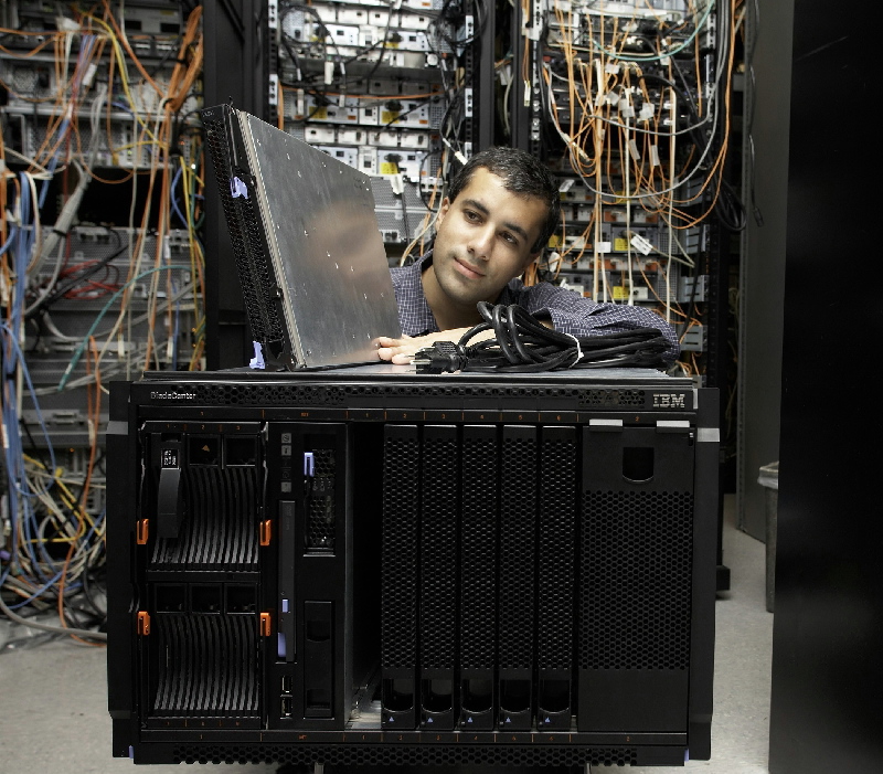 IBM data centre
I’m on the look-out for more. So if you are the media relations for an operator, equipment maker, optical transceiver or component (optical or IC) vendor, can I please request some inspiring photos - ideally with people - and I'll create a photo gallery of the best.
 Network Operations Centre (NOC) Source: AT&T
 Source: Cisco Systems
 An Intel silicon photonics device
And here is an image of Tokyo's data centre on Flickr
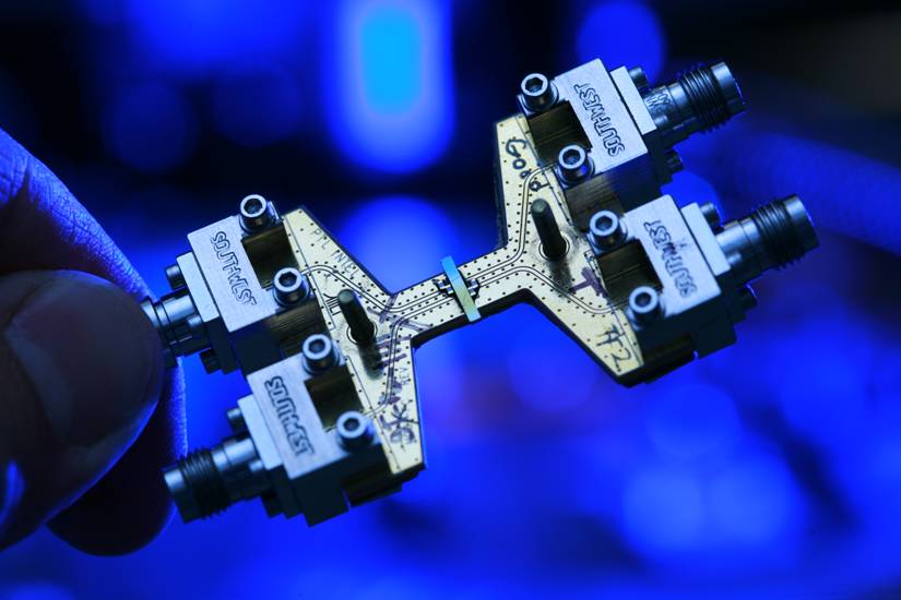
UNIC silicon modulator
This is the silicon photonic start-up’s first announced modulator. The design has been developed in conjunction with Sun Microsystems as part of the DAPRA Ultraperformance Nanophotonic Intrachip Communications (UNIC) programme.
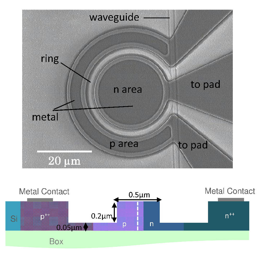 An image of the modulator and a cross-section diagram of the ring waveguide. Source: Kotura
Why is it important?
Optical components use a range of specialist, expensive materials. Silicon is one material that could transform the economics for optics. But for this to happen, the main optical functions – light generation, transmission and detection – need to be supported in silicon. To date, all the required functions except the laser itself - waveguides, modulators and photo-detectors - have been mastered and implemented in silicon.
However, the use of silicon photonics in commercial products has till now been limited. For example, Luxtera makes active optical cable that uses silicon photonics-based transceivers while Kotura has been producing silicon photonics-based VOAs for several years. Its VOA is used within reconfigurable optical add/drop multiplexers (ROADMs) and as a dimmer switch to protect optical receivers from network transients.
Kotura is also supplying its silicon-based Echelle gratings product for 40 and 100 Gigabit Ethernet (GbE) transceiver designs that require the multiplexing and demultiplexing of 4 and 10 wavelengths. The company’s gratings are also being used in Santur’s 100Gbit/s (10x10Gbit/s) transceiver design.
Kotura is in volume production of its VOAs and sampling its Ethernet gratings products, says Arlon Martin, vice-president of marketing and sales at Kotura: “The biggest interest is in 40 Gigabit Ethernet.” Given the small size of the gratings, Kotura is also seeing interest from vendors developing 40GbE transceivers in smaller form factors than the CFP module, such as the QSFP.
This will enable 1Tbit/s data rates over a single fibre to connect high-speed multi-core processor computing elements.
Arlon Martin of Kotura.
But the true potential for silicon photonics, one that promises huge volumes, is very short reach optical interconnects for use in high performance computing and within data centres. Having a low power silicon modulator means it can be integrated with other circuitry in CMOS rather than as a discrete design. Such an integrated approach ensures interconnect reliability.
Method used
There are several ways to modulate a laser. Direct modulation uses electronics to switch the laser on and off at the required rate to imprint the data onto the light. An electro-absorption modulated laser, in contrast, adds an element in front of an always-on laser that either passes or absorbs the light. Kotura’s modulator uses a third approach based on a micro-ring resonator and an adjacent waveguide.
The dimension of the ring – its circumference – dictates when optical resonance occurs. And by carefully matching the power coupling of the micro-ring and waveguide to that of the ring loss, signal attenuation– the light-off condition – is improved. The wavelength at which resonance occurs can be changed by playing with the optical properties of the ring waveguide.
Kotura and Sun have demonstrated the silicon modulator working at up to 11GHz, requiring a peak-to-peak voltage of 2V only. The modulator’s insertion loss is also an attractive 2dB though its working spectrum width is only 0.1nm.
“Our power number – 0.5mW at 10GHz - does not include the driver. But if you want to integrate a number of these on one chip, the low power consumption would enable this,” says Martin. Kotura claims the power consumption achieved is the lowest yet reported.
What next?
The modulator is one of the milestones of the DARPA UNIC programme now into the second of its five-year duration. “This [modulator] is prototype work, not a product,” says Martin, adding that Kotura has not fixed a date as to when the modulator will be commercially used.
As for how the device will ultimately be used, Kotura talks of interfaces operating between 100Gbit/s and 1 Tbit/s. Kotura is already working on an independent programme with CyOptics - the NIST Advanced Technology Programme - developing up to 1Tbit/s links using wavelength division multiplexing (WDM). Such designs use separate laser arrays - each laser at a specific wavelength – as well as gratings and photo-detectors.
In the future inexpensive light sources could generate up to 80 separate modulated lightpaths, Martin says. This will enable 1Tbit/s data rates over a single fibre to connect high-speed multi-core processor computing elements.
Is the idea similar to a broadband light source as proposed for WDM-PON? The UNIC partners have yet to reveal the programme’s detail. “Potentially on the right path,” is all Martin would say.
References:
[1] “Low Vpp, ultralow-energy, compact, high-speed silicon electro-optic modulator.” To read Kotura’s technical paper, click here.
[2] "PHOTONICS APPLIED: INTEGRATED PHOTONICS: Can optical integration solve the computational bottleneck?" OptoIQ, March 1, 2009, click here.
Service providers' network planning in need of an overhaul
These are the findings of an operator study conducted by Analysys Mason on behalf of Amdocs, the business and operational support systems (BSS/ OSS) vendor.
 Columns (left to right): 1) Stove-pipe solutions and legacy systems with no time-lined consolidated view 2) Too much time spent on manual processes 3) Too much time (or too little time) and investment on integration efforts with different OSS 4) Lack of consistent processes or tools to roll-out same resources/ technologies 5) Competition difficulties 6) Delays in launching new services. Source: Analysys MasonClick here to view full chart.
What is network planning?
Every service provider has a network planning organisation, connected to engineering but a separate unit. According to Mark Mortensen, senior analyst at Analysys Mason and co-author of the study, the unit typically numbers fewer than 100 staff although BT’s, for example, has 600.
"They are highly technical; you will have a ROADM specialist, radio frequency experts, someone knowledgeable on Juniper and Cisco routers," says Mortensen. "Their job is to figure out how to augment the network using the available budget."
In particular, the unit's tasks include strategic planning, doing ‘what-if’ analyses two years ahead to assess likely demand on the network. Technical planning, meanwhile, includes assessing what needs to be bought in the coming year assuming the budget comes in.
The network planners must also address immediate issues such as when an operator wins a contract and must connect an enterprise’s facilities in locations where the operator has no network presence.

“What operators did in two years of planning five years ago they are now doing in a quarter.”
Mark Mortensen, Analysys Mason.
Network planning issues
- Operators have less time to plan. “What operators did in two years of planning five years ago they are now doing in a quarter,” says Mortensen. “BT wants to be able to run a new plan overnight.”
- Automated and sophisticated planning tools do not exist. The small size of the network planning group has meant OSS vendors’ attention has been focused elsewhere.
- If operators could plan forward orders and traffic with greater confidence, they could reduce the amount of extra-capacity they currently have in place. This, according to Mortensen, could save operators 5% of their capital budget.
Key study findings
- Changes in budgets and networks are happening faster than ever before.
- Network planning is becoming more complex requiring the processing of many data inputs. These include how fast network resources are being consumed, by what services and how quickly the services are growing.
- As a result network planning takes longer than the very changes it needs to accommodate. “It [network planning] is a very manual process,” says Mortensen.
- Marketing people now control the budgets. This makes the network planners’ task more complex and requires interaction between the two groups. “This is not a known art and requires compromise,” he says. Mortensen admits that he was surprised by the degree to which the marketing people now control budgets.
In summary
Even if OSS vendors develop sophisticated network planning tools, it is unlikely that end users will notice a difference, says Mortensen. However, it will impact significantly operators’ efficiencies and competitiveness.
Users will also not be as frustrated when new service are launched, such as the poor network performance that resulted due to the huge increases in data generated by the introduction of the latest smartphones. This change may not be evident to users but will be welcome nonetheless.

Study details
Analysys Mason interviewed 24 operators including (40%) mobile, (50%) fixed and (10%) cable. A dozen were Tier One operators while two were Tier Three. The rest - Tier Two operators - are classed as having yearly revenues ranging from US$1bn and 10bn. Lastly, half the operators surveyed were European while the rest were split between Asia Pacific and North America. One Latin American operator was also included.
Why optical transceiver vendors are like discus-throwers

Guest blog on Lightwave magazine, click here.