
China and the global PON market
China has become the world's biggest market for passive optical network (PON) technology even though deployments there have barely begun. That is because China, with approximately a quarter of a billion households, dwarfs all other markets. Yet according to market research firm Ovum, only 7% of Chinese homes were connected by year end 2011.

"In 2012, BOSAs [board-based PON optical sub-assemblies] will represent the majority versus optical transceivers for PON ONTs and ONUs"
Julie Kunstler, Ovum
Until recently Japan and South Korea were the dominant markets. And while PON deployments continue in these two markets, the rate of deployments has slowed as these optical access markets mature.
According to Ovum, slightly more than 4 million PON optical line terminals (OLTs) ports, located in the central office, were shipped in Asia Pacific in 2011, of which China accounted for the majority. Worldwide OLT shipments for the same period totaled close to 4.5 million. The fact that in China the ratio of OLT to optical network terminal (ONT), the end terminal at the home or building, deployed is relatively low highlights that in the Chinese market the significant growth in PON end terminals is still to come.
The strength of the Chinese market has helped local system vendors Huawei, ZTE and Fiberhome become leading global PON players, accounting for over 85% of the OLTs sold globally in 2011, says Julie Kunstler, principal analayst, optical components at Ovum. Moreover, around 60% of fibre-to-the-x deployments in Europe, Middle East and Africa were supplied by the Chinese vendors. The strongest non-Chinese vendor is Alcatel-Lucent.
Ovum says that the State Grid China Corporation, the largest electric utility company in China, has begun to deploy EPON for their smart grid trial deployments. PON is preferred to wireless technology because of its perceived ability to secure the data. This raises the prospect of two separate PON lines going to each home. But it remains to be seen, says Kunstler, whether this happens or whether the telcos and utilities share the access network.
"After China the next region that will have meaningful numbers is Eastern Europe, followed by South and Central America and we have already seen it in places like Russia,” says Kunstler. Indeed FTTx deployments in Eastern Europe already exceed those in Western Europe.
EPON and GPON
In China both Ethernet PON (EPON) and Gigabit PON (GPON) are being deployed. Ovum estimates that in 2011, 65% of equipment shipments were EPON while GPON represented 35% GPON in China.
China Telecom was the first of the large operators in China to deploy PON and began with EPON. Ovum is now seeing deployments of GPON and in the 3rd quarter of 2012, GPON OLT deployments have overtaken EPON.
China Mobile, not a landline operator, started deployments later and chose GPON. But these GPON deployments are on top of EPON, says Kunstler: "EPON is still heavily deployed by China Telecom, while China Mobile is doing GPON but it is a much smaller player." Moreover, Chinese PON vendors also supplying OLTs that support EPON and GPON, allowing local decisions to be made as to which PON technology is used.
One trend that is impacting the traditional PON optical transceiver market is the growing use of board-based PON optical sub-assemblies (BOSAs). Such PON optics dispenses with the traditional traditional optical module form factor in the interest of trimming costs.
“A number of the larger, established ODMs [original design manufacturers] have begun to ship BOSA-based PON CPEs,” says Kunstler. In 2012, BOSAs will represent the majority versus optical transceivers for PON ONTs/ONUs.” says Kunstler.
10 Gigabit PON
Ovum says that there has been very few deployments of next generation 10G EPON and XG-PON, the 10 Gigabit version of GPON.
"There have been small amounts of 10G [EPON] in China," says Kunstler. "We are talking hundreds or thousands, not the tens of thousands [of units]."
One reason for this is the relative high cost of 10 Gigabit PON which is still in its infancy. Another is the growing shift to deploy fibre-to-the-home (FTTh) versus fibre-to-the-building deployments in China. 10 Gigabit PON makes more sense in multi-dwelling units where the incoming signal is split between apartments. Moving to 10G EPON boosts the incoming bandwidth by 10x while XG-PON would increase the bandwidth by 4x. "The need for 10 Gig for multi-dwelling units is not as strong as originally thought," says Kunstler.
It is a chicken-and-egg issue with 10G PON, says Kunstler. The price of 10G optics would go down if there was more demand, and if there was more demand, the optical vendors would work on bringing down cost. "10G GPON will happen but will take longer," says Kunstler, with volumes starting to ramp from 2014.
However, Ovum thinks that a stronger market application for 10G PON will be for supporting wireless backhaul. The market research company is seeing early deployments of PON for wireless backhaul especially for small cell sites (e.g. picocells). Small cells are typically deployed in urban areas which is where FTTx is deployed. It is too early to know the market forecast for this application but PON will join the list of communications technologies supporting wireless backhaul.
Challenges
Despite the huge expected growth in deployments, driven by China, challenges remain for PON optical transceiver and chip vendors.
The margins on optics and PON silicon continue to be squeezed. ODMs using BOSAs are putting pricing pressure on PON transceiver costs while the vertical integration strategy of system vendors such as Huawei, which also develops some of its own components squeezes, out various independent players. Huawei has its own silicon arm called HiSilicon and its activities in PON has impacted the chip opportunity of the PON merchant suppliers.
"Depending upon who the customer is, depending upon the pricing, depending on the features and the functions, Huawei will make the decision whether they are using HiSilicon or whether they are using merchant silicon from an independent vendor, for example," says Kunstler.
There has been consolidation in the PON chip space as well as several new players. For example, Broadcom acquired Teknouvs and Broadlight while Atheros acquired Opulan and Atheros was then acquired by Qualcomm. Marvell acquired a very small start-up and is now competing with Atheros and Broadcom. Most recently, Realtek is rumored to have a very low-cost PON chip.
Avago's latest optical engine targets active optical cables
Avago Technologies has unveiled its first family of active optical cables for use in the data centre and for high performance computing.
The company has developed an optical engine for use in the active optical cables (AOCs). Known as the Atlas 75x, the optical engine reduces the power consumption and cost of the AOC to better compete with direct-attach copper cables.

“Some 99 percent of [active optical cable] applications are 20m or less”
Sharon Hall, Avago
"This is a price-elastic market," says Sharon Hall, product line manager for embedded optics at Avago Technologies. "A 20 percent price premium over a copper solution, then it starts to get interesting."
The AOC family comprises a 10 Gigabit-per-second (Gbps) single channel SFP+ and two QSFP+ cables - a 4x10Gbps QSFP+ and a QSFP+-to-four SFP+. The SFP+ AOC is used for 10 Gigabit Ethernet, 8 Gigabit Fibre Channel and Infiniband applications. The QSFP+ is used for 4-channel Infiniband, serial-attached SCSI (SAS) storage while the QSFP-to-four-SFP+ is required for server applications.
There are also three 12-channel CXP AOC products: 10-channel and 12-channel cables with each channel at 10Gbps; and a 12-channel CXP, each at 12.5Gbps. The devices supports the 100GBASE-SR10 100 Gigabit Ethernet and 12-channel Infiniband standards.
The 12-channel 12.5Gbps CXP product is used typically for proprietary applications such as chassis-to-chassis links where greater bandwidth is required, says Avago.
The SFP+ and QSFP+ products have a reach of 20m whereas competing AOC products achieve 100m. “Some 99 percent of applications are 20m or less,” says Hall.
The SFP+ and QSFP+ AOC products use the Atlas 75x optical engine. The CXP cable uses Avago’s existing Atlas 77x MicroPod engine and has a reach of 100m.
The Atlas 75x duplex 10Gbps engine reduces the power consumption by adopting a CMOS-based VCSEL driver instead of a silicon germanium one. “With CMOS you do not get the same level of performance as silicon germanium and that impacts the reach,” says Hall. “This is why the MicroPod is more geared for the high-end solutions.”
The result of using the Atlas 75x is an SFP+ AOC with a power consumption of 270mW compared to 200mW of a passive direct-attach copper cable. However, the SFP+ AOC has a lower bit error rate (1x10-15 vs. 1x10-12), a reach of up to 20m compared to the copper cable’s 7m and is only a quarter of the weight.
The SFP+ AOC does have a lower power consumption compared to active direct-attach cable, which consumes 400-800mW and has a reach of 15m.
Avago says that up to a 30m reach is possible using the Atlas 75x optical engine. Meanwhile, samples of the AOCs are available now.
Infinera adds software to its PIC for instant bandwidth
Infinera has enabled its DTN-X platform to deliver rapidly 100 Gigabit services. The ability to fulfill capacity demand quickly is seen as a competitive advantage by operators. Gazettabyte spoke with Infinera and TeliaSonera International Carrier, a DTN-X customer, about the merits of its 'instant bandwidth' and asked several industry analysts for their views.
 Infinera has added a WDM line card hosting its 500 Gigabit super-channel photonic integrated circuit to its DTN-X platform
Pravin Mahajan, Infinera.
Infinera is claiming an industry first with the software-enablement of 100 Gigabit capacity increments. The company's DTN-X platform's 'instant bandwidth' feature shortens the time to add new capacity in the network, from weeks as is common today to less than a day.
The ability to add bandwidth as required is increasingly valued by operators. TeliaSonera International Carrier points out that its traffic demands are increasingly variable, making capacity requirements harder to forecast and manage.
"It [the DTN-X's instant bandwidth] enables us to activate 100 Gig services between network spans to manage our own IP traffic which is growing rapidly," says Ivo Pascucci, head of sales, Americas at TeliaSonera International Carrier. "We will also be able to sell in the market 100 Gig services and activate the capacity much more rapidly."
What has been done
Infinera has added three elements to enable its DTN-X platform to enable 100 Gigabit services.
One is a new wavelength division multiplexing (WDM) line card that features its 500 Gigabit-per-second (Gbps) super-channel photonic integrated circuit (PIC). Infinera says the line card has 500Gbps of capacity enabled, of which only 100Gbps is activated. "The remaining 400Gbps is latent, waiting to be activated," says Pravin Mahajan, director of corporate marketing and messaging at Infinera.
Infinera uses the DTN-X's Optical Transport Network (OTN) switch fabric to pack the client side signals onto any of the 100Gbps channels activated on the line side. This capacity pool of up to 500 Gbps, says Infinera, results in better usage of backbone capacity compared to traditional optical networking equipment based on individual 100Gbps 'siloed' channels.
A software application has also been added to Infinera's network management system, the digital network administrator (DNA), to activate the 100Gbps capacity increments.
Lastly, Infinera has in place a just-in-time system that enables client-side 10 Gigabit Ethernet optical transceivers to be delivered to customers within 10 days, if they out of stock. Infinera says it is achieving a 6-day delivery time in 95% of the cases.

Advantages
TeliaSonera International Carrier confirms the advantages to having 100 Gigabit capacities pre-provisioned and ready for use.
 "Having the ability to turn up large bandwidth is critical to our business, especially as the [traffic] numbers continue to grow"
Ivo Pascucci, TeliaSonera International Carrier
"If it is individual line cards across the network when you have as many PoPs as we do, it does get tricky," says Pascucci. "If we have 500 Gig channels pre-provisioned with the ability to activate 100 Gig segments as needed, that gives us an advantage versus having to figure out how many line cards to have deployed in which nodes, and forecasting which nodes should have the line cards in the first place."
The operator is already seeing demand for 100 Gigabit services, from the carrier market and large content providers. The operator already provides 10x10Gbps and 20x10Gbps services to customers. "With that there are all the challenges of provisioning ten or 20 10 Gig circuits and 10 or 20 cross-connects for each site," says Pascucci. The operator also manages one and two Terabits of network capacity for certain customers.
"Having the ability to turn up large bandwidth is critical to our business, especially as the [traffic] numbers continue to grow," says Pascucci.
Analysts' comments
Gazettabye asked several industry analysts about the significance of Infinera's announcement. In particular the uniqueness of the offering, the claim to reduce rapidly bandwidth enablement times and its importance for operators.
Infonetics Research
Andrew Schmitt, directing analyst for optical
Schmitt believes Infinera's announcement is significant as it is the first announced North American win. It also shows the company has a solution for carriers that only want to roll out a single 100 Gbps but don't want to buy 500Gbps.

More importantly, it should allow some carriers to deploy extra capacity for future use at no cost to them and that opens up interesting possibilities for automatically switched optical network (ASON) management or even software-defined networking (SDN).
"As to the claim that it reduces capacity enablement from weeks to potential minutes, to some degree, yes," says Schmitt.
Certainly Ciena, Alcatel-Lucent or Cisco could ship extra line cards into customers and not charge the customer until they are used and that would effectively achieve the same result. "But if the PIC truly has better economics than the discrete solutions from these vendors then Infinera can ship hardware up front and then recognise the profits on the back end," he says.
"You simply can't predict where the best places to put bandwidth will be"
In turn, if customers get free inventory management out of the deal and Infinera equipment can support that arrangement more economically, that is a significant advantage for Infinera.
"This instant bandwidth is unique to Infinera. As I said, anyone could do this deal. But you need a hardware cost structure that can support it or it gets expensive quickly," says Schmitt. "Everyone is working on super-channels but it is clear from the legacy of the way the 10 Gig DTN hardware and software worked that Infinera gets it."
Schmitt believes the term super-channel is abused. He prefers the term virtualised bandwidth - optical capacity that can be allocated the same way server or storage resources are assigned through virtualization.
"The SDN hype is hitting strong in this business but Infinera is really one of the only companies that have a history of a hardware and software architecture that lends itself well to this concept," he says. This is validated with its customer list which is loaded heavily with service providers that are not just talking about SDN but actively doing something, he says.
"It [turning capacity up quickly] is important for SDN as well as more advanced protection arrangements. You simply can't predict where the best places to put bandwidth will be," says Schmitt. "If you can have spare capacity in the network that is lit on demand but not paid for if you don't need it, it is the cheapest approach for avoiding overbuilding a network for corner-case requirements.
"I think the accounting for this product will be interesting, it is likely that we will know in a year how successful this concept was just by a careful examination of the company's financials," he concludes.
ACG Research
Eve Griliches, vice president of optical networking
Infinera delivered this year the DTN-X with 500 Gig super-channels based on PIC technology. Now, a new 500 Gig line card has been added that can operate at 100 Gig and the remaining 400 Gig can be lit in 100 Gig increments using software. This allows customers to purchase 100 Gig at a time, and turn up subsequent bandwidth via software when they require it.

“No other vendor has a software-based solution, and no one else is delivering 500 Gig yet either,” says Griliches.
With this solution, ACG Research says in its research note, operators can start to develop a flexible infrastructure where bandwidth can grow and move around the network instantly. This is useful to address varying demands in bandwidth, triggered by incidents such as natural disasters or sporting events.
Rapid bandwidth enablement has always been important and takes way too long, so this development is key, says Griliches: “Also, it enables Infinera to enter markets which only need one 100 Gig wavelength for now, which they could not do before.”
“No other vendor has a software-based solution, and no one else is delivering 500 Gig yet either”
Looking forward, ACG Research expects this software and hardware-based instant bandwidth utility model will enable Infinera to widen its potential market base and increase its global market share in 2013 and 2014.
Ovum
Ron Kline, principal analyst, and Dana Cooperson, vice president, of the network infrastructure practice
Ovum also thinks Infinera's announcement is significant. It brings essentially the same value proposition Infinera had with 10 Gigabit to the 100 Gigabit market - low operational expenditure (opex) and quick time-to-market. ”Remember 10 Gig in 10 days?” says Kline.

It further fixes an issue for customers in that with the 10x10Gbps, they had to essentially pay for the full 100Gbps up front, and then they could be very efficient with turn-up and opex. Customers made an efficient opex for more capital expenditure (capex) up-front trade. "With instant bandwidth, they don't have to make the upfront capex-versus-opex tradeoff; they can be most efficient with both,” says Cooperson.
Any vendor can shorten capacity enablement times if they can convince the operator to pre-position bandwidth in the network that is ready to be turned on at a moment's notice.
Ron Kline
Kline says operators has different processes for turning up services and in many cases it is these processes and not the equipment directly that is the cause of the additional time for provisioning. “For example the operator may not use the DNA system or may have a very complex OSS/BSS used in the process,” says Kline.
Nevertheless, the capability to have really short provisioning is there, if an operator wants to take advantage. In the TeliaSonera case, Infinera is managing the network so the quick time to market will be there, says Kline.
Cooperson adds that there can be many factors that impede the capacity enablement process, based on Ovum's own research. “But it is clear from talking to Infinera's customers that its system design and approach is a big benefit to those carriers, often the competitive carriers, in competing in the market,” she says. “Multiple carriers told us that with the Infinera system, they were able to win business from competitors.”

Any vendor can shorten capacity enablement times if they can convince the operator to pre-position bandwidth in the network that is ready to be turned on at a moment's notice. However what is unique to Infinera is its system is deployed 500Gbps at a time and all the switching is done electrically by the OTN switch at each node. Others are working on super-channels but none are close to deploying, says Ovum.
“Multiple carriers told us that with the Infinera system, they were able to win business from competitors.”
Dana Cooperson
The ability to turn on bandwidth rapidly is becoming increasingly important. From a wholesale operator perspective it is very important and a key differentiator.
"It's particularly relevant to wholesale applications where large bandwidth chunks are required and the customer is another carrier," says Cooperson. "Whether you view a Google or a Facebook as a carrier or a very large enterprise, it would apply to them as well as a more traditional carrier."
VDSL2 vectoring explained
Several system vendors including Adtran, Alcatel-Lucent and ZTE have announced vectoring technology that boosts the performance of very-high-bit-rate digital subscriber line (VDSL2) broadband access technology. Vectoring is used to counter crosstalk - signal leakage between the telephony twisted wire pairs that curtails VDSL2's bit rate performance – as is now explained.
Technology briefing
 There is a large uncertainty in the resulting VDSL2 bit rate for a given loop length. With vectoring this uncertainty is almost removed
Paul Spruyt, Alcatel-Lucent
Two key characteristics of the local loop limit the performance of digital subscriber line (DSL) technology: signal attenuation and crosstalk.
Attenuation is due to the limited spectrum of the telephone twisted pair, designed for low frequency voice calls not high-speed data transmission. Analogue telephony uses only 4kHz of spectrum, whereas ADSL uses 1.1MHz and ADSL2+ 2.2MHz. The even higher speed VDSL2 has several flavours: 8b is 8.5MHz, 17a is 17.6MHz while 30a spans 30MHz.
The higher frequencies induce greater attenuation and hence the wider the spectrum, the shorter the copper loop length over which data can be sent. This is why higher speed VDSL2 technology requires the central office or, more commonly, the cabinet to be closer to the user, up to 2.5km away - although in most cases VDSL2 is deployed on loops shorter than 1.5km.
The second effect, crosstalk, describes the leakage of the signal in a copper pair into neighbouring pairs. “All my neighbours get a little bit of the signal sent on my pair, and vice versa: the signal I receive is not only the useful signal transmitted on my pair but also noise, the contributed components from all my active VDSL2 neighbours,” says Paul Spruyt, xDSL technology strategist at Alcatel-Lucent.
Typical a cable bundle comprises several tens to several hundred copper pairs. The signal-to-noise ratio on each pair dictates the overall achievable data rate to the user and on short loops it is the crosstalk that is the main noise culprit.
Vectoring boosts VDSL2 data rates to some 100 megabits-per-second (Mbps) downstream and 40Mbps upstream over 400m. This compares to 50Mbps and 20Mbps, respectively, without vectoring. There is a large uncertainty in the resulting VDSL2 bit rate for a given loop length. "With vectoring this uncertainty is almost removed," says Spruyt.
Vectoring
The term vectoring refers to the digital signal processing (DSP) computations involved to cancel the crosstalk. The computation involves multiplying pre-coder matrices with Nx1 data sets – or vectors – representing the transmit signals.
The crosstalk coupling into each VDSL2 line is measured and used to generate an anti-noise signal in the DSLAM to null the crosstalk on each line.
To calculate the crosstalk coupling between the pairs in the cable bundle, use is made of the ‘sync’ symbol that is sent after every 256 data symbols, equating to a sync symbol every 64ms or about 16 a second.
Each sync symbol is modulated with one bit of a pilot sequence. The length of the pilot sequence is dependent on the number of VDSL2 lines in the vectoring group. In a system with 192 VDSL2 lines, 256-bit-long pilot sequences are used (the next highest power of two).
Moreover, each twisted pair is assigned a unique pilot sequence, with the pilots usually chosen such that they are mutually orthogonal. “If you take two orthogonal pilots sequences and multiply them bit-wise, and you take the average, you always find zero,” says Spruyt. "This characteristic speeds up and simplifies the crosstalk estimation.”
A user's DSL modem expects to see the modulated sync symbol, but in reality sees a modulated sync symbol distorted with crosstalk from the modulated sync symbols transmitted on the neighbouring lines. The modem measures the error – the crosstalk – and sends it back to the DSLAM. The DSLAM correlates the received error values on the ‘victim’ line with the pilot sequences transmitted on all other ‘disturber’ lines. By doing this, the DSLAM gets a measure of the crosstalk coupling for every disturber – victim pair.
The final step is the generation of anti-noise within the DSLAM.
This anti-noise is injected into the victim line on top of the transmit signal such that it cancels the crosstalk signal picked up over the telephone pair. This process is repeated for each line.
 Source: Alcatel-Lucent
VDSL2 uses discrete multi-tone (DMT) modulation where each DMT symbol consists of 4096 tones, split between the upstream (from the DSL modem to the DSLAM) and the downstream (to the user) transmissions. All tones are processed independently in the frequency domain. The resulting frequency domain signal including the anti-noise is converted back to the time domain using an inverse fast Fourier transform.
The above describes the crosstalk pre-compensation or pre-coding in the downstream direction: anti-noise signals are generated and injected in the DSLAM prior to transmission of the signal on the line.
For the upstream, the inverse occurs: the DSLAM generates and adds the anti-noise after reception of the signal distorted with crosstalk. This technique is known as post-compensation or post-coding. In this case the DSL modem sends the pilot modulated sync symbols and the DSLAM measures the error signal and performs the correlations and anti-noise calculations.
Challenges
One key challenge is the amount of computations to be performed in real-time. For a fully-vectored 200-line VDSL2 system, some 2,600 billion multiply-accumulates per second - 2.6TMAC/s - need to be calculated. A system of 400 lines would require four times as much processing power, about 10TMAC/s.
Alcatel-Lucent’s first-generation vectoring system that was released end 2011 could process 192 lines. At the recent Broadband World Forum show in October, Alcatel-Lucent unveiled its second-generation system that doubles the capacity to 384 lines.
For larger cable bundles, the crosstalk contributions from certain more distant disturbers to a victim line are negligible. Also, for large vectoring systems, pairs typically do not stay together in the same cable but get split over multiple smaller cables that do not interfere with each other. “There is a possibility to reduce complexity by sparse matrix computations rather than a full matrix,” says Spruyt, but for smaller systems full matrix computation is preferred as the disturbers can’t be ignored.
There are other challenges.
There is a large amount of data to be transferred within the DSLAM associated with the vectoring. According to Alcatel-Lucent, a 48-port VDSL2 card can generate up to 20 Gigabit-per-second (Gbps) of vectoring data.
There is also the need for strict synchronization – for vectoring to work the DMT symbols of all lines need to be aligned within about 1 microsecond. As such, the clock needs to be distributed with great care across the DSLAM.
Adding or removing a VDSL2 line also must not affect active lines which requires that crosstalk is estimated and cancelled before any damage is done. The same applies when switching off a VDSL2 modem which may affect the terminating impedance of a twisted pair and modify the crosstalk coupling. Hence the crosstalk needs to be monitored in real-time.
Zero touch
A further challenge that operators face when upgrading to vectoring is that not all the users' VDSL2 modems may support vectoring. This means that crosstalk from such lines can’t be cancelled which significantly reduces the vectoring benefits for the users with vectoring DSL modems on the same cable.
To tackle this, certain legacy VDSL2 modems can be software upgraded to support vectoring. Others, that can't be upgraded to vectoring, can be software upgraded to a ‘vector friendly’ mode. Crosstalk from such a vector friendly line into neighbouring vectored lines can be cancelled, but the ‘friendly’ line itself does not benefit from the vectoring gain.
Upgrading the modem firmware is also a considerable undertaking for the telecom operators especially when it involves tens or hundreds of thousands of modems.
Moreover, not all the CPEs can be upgraded to friendly mode. To this aim, Alcatel Lucent has developed a 'zero-touch' approach that allows cancelling the crosstalk from legacy VDSL2 lines into a vectored lines without CPE upgrade. “This significantly facilitates and speeds up the roll-out of vectoring” says Spruyt
Further reading:
Boosting VDSL2 Bit Rates with Vectoring
DSL: Will phantom channels become real deployments
ECOC 2012 summary - Part 2: Finisar
Gazettabyte completes its summary of key optical announcements at the recent ECOC show held in Amsterdam. In Part 2, Finisar's announcements are detailed.
Part 2

"The general thought with system vendors is that the more they can shrink the in-line equipment into a fewer number of slots, the more slots they have open and available for revenue-generating transceiver and transponder cards"
Rafik Ward, Finisar
Finisar showed its board-mounted parallel optics module in use within a technology demonstrator from data storage firm Xyratex, showcased what it claims is the industry's first two-slot reconfigurable optical add/ drop multiplexer (ROADM) design, unveiled its first CFP2 pluggable transceiver and announced its latest WaveShaper products.
The data storage application uses Finisar's vertical-cavity surface-emitting laser (VCSEL)-based board mounted optical assembly. The optical assembly - or optical engine - comprises 24-channels, 12 transmitters and 12 receivers.
The optical engine sits on the board and is used for such applications as chip-to-chip interconnect, optical backplanes, and dense front panels, and supports a variety of protocols. These include PCI Express, Ethernet and Infiniband as well as proprietary schemes. Indeed the only limit is the VCSEL speed. The optical engine is designed to support traffic up to 28 Gigabit-per-second (Gbps) per channel, once 28 Gigabit VCSELs become available. Finisar have already demonstrated working 28Gbps VCSELs.
The ECOC demonstration showed the optical engine in use within Xyratex's demonstrator storage system. "They are carrying traffic between internal controller cards and the traffic being carried is 12-Gig SAS [serial attached SCSI]," says Rafik Ward, vice president of marketing at Finisar.
As well as the optical engine, the demonstration included polymer waveguides from Vario-optics which connect the optical engine to a backplane connector, built by Huber + Suhner, as well as SAS silicon from LSI.
Finisar first showed the waveguide and connector technologies in a demonstration at OFC 2012. "This is an early prototype but it's a very exciting one," says Ward. "It shows all elements of the ecosystem coming together and running in a live system."

Finisar also showcased what it claims is the industry's first two-slot ROADM line card. The line card was part of a Cisco Systems' platform, according to one analyst shown the demonstration.
The company-designed card uses a high port-count wavelength-selective switch (WSS) that enables both add and drop traffic. "We have built transmit and receive into the same line card using a high port-count device," says Ward. Finisar is not detailing the exact WSS used or how the system is implemented but describes it as a flexible spectrum, 2x1x17 port line card.
The advantage of a denser ROADM line card is that it frees up slots in a system vendor's chassis. A slot can be used for either in-line equipment - WSSes and amplifiers - or terminal equipment that host the transceivers and transponders.
"It is like valuable real-estate," says Ward. "The general thought with system vendors is that the more they can shrink the in-line equipment into a fewer number of slots, the more slots they have open and available for revenue-generating transceiver and transponder cards."
The company also detailed its first CFP2 100 Gigabit optical transceiver. The CFP2 uses a single TOSA comprising four distributed feedback (DFB) lasers, a shared thermo-electric cooler and the multiplexer. The CFP2 consumes under 8W by using the DFBs and an integrated transceiver optical sub-assembly (TOSA).
ECOC 2012 summary - Part 1: Oclaro
Gazettabyte completes its summary of key optical announcements at the recent ECOC show held in Amsterdam. Oclaro's announcements detailed here are followed by those of Finisar and NeoPhotonics.
Part 1: Oclaro

"Networks are getting more complex and you need automation so that they are more foolproof and more efficient operationally"
Per Hansen, Oclaro
Oclaro made several announcements at ECOC included an 8-port flexible-grid optical channel monitor, a new small form factor pump laser MSA and its first CFP2 module. The company also gave an update regarding its 100 Gigabit coherent optical transmission module as well as the company's status following Oclaro's merger with Opnext (see below).
The 8-port flexible grid optical channel monitor (OCM) is to address emerging, more demanding requirements of optical networks. "Networks are getting more complex and you need automation so that they are more foolproof and more efficient operationally," says Per Hansen, vice president of product marketing, optical networks solutions at Oclaro.
The 8-port device can monitor up to eight fibres, for example the input and seven output ports of a wavelength-selective switch or an amplifier's outputs.
The programmable OCM can do more than simply go from fibre to fibre, measuring the spectrum. The OCM can dwell on particular ports, or monitor a wavelength on particular ports when the system is adjusting or turning up a wavelength, for example.
"There is processing power included such that you can do a lot of data processing which can then be exported to the line card in the format required," says Hansen. This is important as operators start to adopt flexible-grid network architectures. "[With flexible-grid spectrum] you don't know where channels stop and start such that an OCM that looks at fixed slots in no longer enough," says Hansen.
The OCM can monitor bands finer than 6.25GHz through to the spectrum across the complete C-band.
Oclaro also detailed that its OMT-100 coherent 100 Gigabit optical module is entering volume production. "We have shipped well over 100 [units] to various customers," says Hansen. "There are a lot of system houses looking at this type of module this year." The OMT-100 was developed by Opnext and replaces Oclaro's own MI 8000XM 100 Gigabit module
The company also announced its first 100 Gigabit CFP2 module and its second-generation CFP module 16W power consumption that support the IEEE 100GBASE-LR4 10km standard.
A new small form factor multi-source agreement (MSA) for pump laser diodes was also announced at the show, involving Oclaro and 3S Photonics.
The 10-pin butterfly package is designed to replace the existing 14-pin design. "It is 75% smaller in volume - about two-thirds in each dimension," says Robert Blum, director of product marketing for Oclaro's photonic components. The MSA supports a single cooled or uncooled pump laser, and its smaller volume enables more integrated amplifier designs.
Oclaro says other companies have expressed interest in the MSA and it expects additional players to join.
The New Oclaro
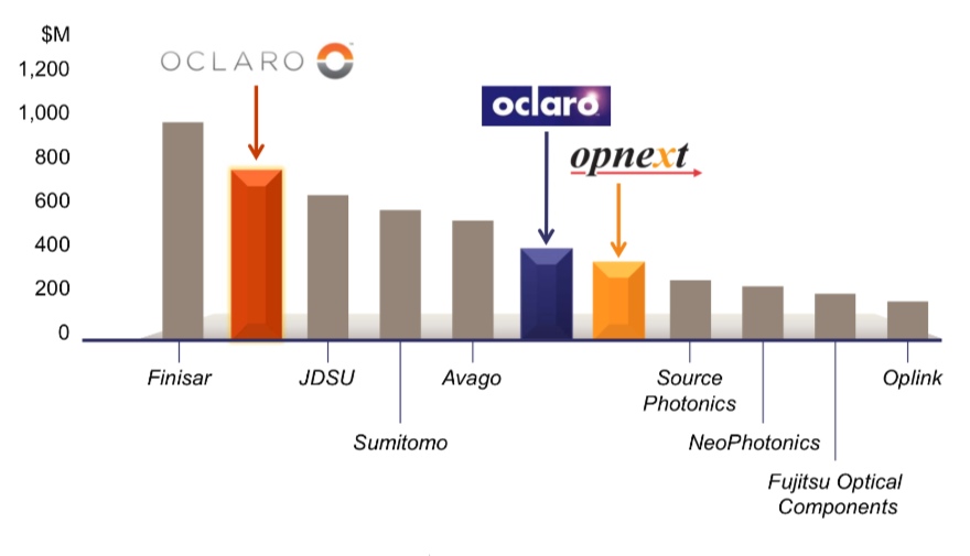
Source: Ovum
Oclaro also gave an update of the company's status following the merger with Opnext earlier this year. The now 3,000-strong company has estimated annual revenues of US $800m. This places the optical component company second only to Finisar.
The merger has broadened the company's product line, adding Opnext's strength in datacom pluggable transceivers to Oclaro's core networking products. The company is also more vertically integrated, using its optical components such as tunable laser and VCSEL technologies, modulators and receivers within its line-side transponders and pluggable optical transceivers.
"You can drive technologies in different directions and not just be out there buying components and throwing them together," says Hansen.
The company also has a range of laser diodes for industrial and consumer applications. "We [Oclaro] were already the largest merchant supplier of high-power laser diodes but now we have a complete portfolio that covers all the wavelengths from 400 up to 1500nm," says Blum.
The company has a broad range of technologies that include indium phosphide, gallium arsenide, lithium niobate, MEMS, liquid crystal and gallium nitride.
An extra business unit has also been created. To the existing optical networks solutions and the photonic components businesses there is now the modules and devices unit covering pluggable and high-speed client side transceivers, and which is based in Japan.
Q&A with Kotura's CTO: Integration styles and I/O limits
The second, and final part, of the Q&A with Mehdi Asghari, CTO of silicon photonics start-up, Kotura.
Part 2 of 2

"When do the big players adopt a new technology and go from an electrical to an optical solution? In my experience, usually when they absolutely have to."
Mehdi Asghari, CTO, Kotura
Q: Silicon photonics comes in two integration flavours: the monolithic approach where the modulators and detectors are implemented monolithically while the lasers are coupled externally (e.g. Kotura and Luxtera); and heterogeneous integration where III-V materials such as indium phosphide are bonded to the silicon to form a hybrid design yet are grown on a single die (e.g. Aurrion). Does one approach have an advantage?
A: I have a III-V background and converted to silicon photonics over 15 years ago. The key issue here is what are you trying to do? Why are we going from III-V processing to silicon? Is it the yield and process maturity or the device performance for actives?
If it is the former, then heterogeneous integration does not really solve the problem since you are still processing III-V devices and are likely to need multiple fabs to do it. If it is the latter then you should stick to III-V wafers.
The fact is that silicon provides passive performance that is far superior to III-V while the active performance – the detector and modulator - is good enough. In fact our germanium detectors could be better and our electro-absorption modulators can be lower power and exhibit a broader working spectral range.
We have seen repeatedly that being good enough is all that silicon has to show it can do to win and that it is certainly doing.
"It is not enough to offer a 10%, 20% or even a 50% cost saving when you are offering the customer a brand new solution that comes with all the risks and unknowns associated with that technology."
Kotura has developed components for telecom (variable optical attenuators, and the functions needed for a 100 Gig coherent receiver) yet its focus is on datacom. Why is that?
We started in telecom as we looked for low hanging fruit that could give us a good margin and an easy start in our early days. This is important for a start-up with a new technology. The well-entrenched incumbent technologies are hard to displace.
You have to find an application with a clear value proposition to get started. Once you have established yourself, your supply chain and manufacturing infrastructure, you can take on more challenging and larger market opportunities.
We see certain areas in datacom that are not well served by either the short reach optics or the telecom grade solutions. Extended reach data centre is one key area where short-reach optics based on VCSELs cannot cover the reach needed and conventional telecom solutions are inherently over-engineered and do not meet the power, cost and size needed.
We think silicon photonics can play a key role here as a starting point in datacom. A key advantage of our platform here is that we can do WDM [wavelength division multiplexing] and hence offer 100 Gig on a single fibre (per direction). This is a major cost saving for longer reaches (>>50m) deployed in such links.
There are some big system players with silicon photonics (Cisco Systems, Alcatel-Lucent) and several small merchant silicon photonics players, such as the companies mentioned in the previous question, which must develop products to sell while funding the development of their technologies. How do you expect the silicon photonics marketplace to evolve, especially now that the technology is being more widely embraced?
For silicon photonics to succeed commercially, we need a multitude of vibrant and successful players in the field. Some of these can be start-ups that lead the innovation in technology and manufacturing but others can be larger organisations that have invested to service an internal need or leverage an existing dominance in the market.
There is room and a necessity for both. It takes a village to raise a child. One single company will not turn silicon photonics into a successful commercial reality.
Cisco Systems has been talking about its proprietary CPAK transceiver. Here is an example of a system vendor using in-house silicon photonics for its own use. Why do you think about such a development? And is Kotura being approached by equipment vendors that want to work with you to develop a custom design?
It is not new for a large company like Cisco to try and make sure that is has its own proprietary components to go into its systems to protect their product and their margins. We see that in all industries.
In terms of other companies coming up with their own proprietary solutions, we do see more and more of this - and a lot more this year than last year - especially when you come off the telecom bandwagon and into the datacom environment: data centres and high-performance computing.
That is because the customer is in charge of the entire environment, the two ends of the link, they can leverage more value from the solution you have to offer without worrying about standards. This is one way for systems companies to leverage value from components.
People are starting to see that the conventional technologies they have deployed are hitting a wall. When they are deploying a new solution they are rethinking their hardware strategy, and how they leverage it to add more value and differentiation to their system.
New ways to architect systems are becoming possible. If you are able to avoid limitations such as distance between the processor and memory, the router and switches and so on, you can come up with a very different architecture for your system and solution.
When do the big players adopt a new technology and go from an electrical to an optical solution? In my experience, usually when they absolutely have to. Most people don't adopt a new solution until they really, really need to; when the value proposition completely outweighs the risk.
It is not enough to offer a 10%, 20% or even a 50% cost saving when you are offering the customer a brand new solution that comes with all the risks and unknowns associated with that technology.
You have to offer them something new, to enable a new application, to add value by enabling a feature, something they can leverage in their product.
When you say systems people adopt new technology when they hit a wall, can you highlight examples of these hurdles?
When you look at the adoption of optics coming from the copper-dominated connectivity, it is very interesting.
Originally, for optics to work its way into the copper world, it had to hide itself and look like a copper solution. People had no idea how to create connectors and they were worried about fibre. So it was disguised as a copper solution.
As customers have got used to it, we can now come out and be more open. We can now do more innovative things with optical transceivers. If you look at the adoption rate, it is being accelerated by customers' demand such as 25 Gigabit signalling.
We can see that the processors and the ASICs - a switch from Broadcom or a processor from Intel or AMD - they are running into I/O [input/ output] density bottlenecks. The chip area is pretty constant, the packages are about the standard size, the number of pins are going beyond what they can support, they have to ramp up the pin rate to about 25 Gigabit-per-second (Gbps), while there are also some 10Gbps pins.
But the number of 25Gbps pins are becoming so high, potentially many hundreds, that they are not going to be able to trace them into the PCB (printed circuit board). The PCB can only take a 25Gbps signal for about 4 inches (~10cm) and then you need serdes [serialiser/ deserialiser) and repeaters.
You may imagine a current router or switch ASIC having ten 25Gbps pins and 100 10Gbps pins. The 10Gbps pins I can take to the edge and use 10Gbps transceivers; and the ten 25Gbps pins I can still do something about it. I may need a lot of electronics and serdes, and use pre-emphasis and equalisation.
But the next generation, when it becomes 100 25Gbps pins, you just cannot do that at the board level. That is where we will start to have to use optics close to the chip.
Will they go for very compact transceivers that sit next to the ASIC or would they try and co-package it with the ASIC?
My perception is that the first generation will be next to the ASIC. People will not integrate an unknown technology into a multi-billion dollar business, they will hedge their bets and have an external solution that offers them some level of assurance that if one solution does not work, they can change to another. But once they get used to it, they can start to integrate these in a multi-chip module solution.
What are the timescales?
I see transceivers next to the ASICs being deployed around 2017-18, maybe a bit sooner, with the co-packaging around 2018-20. People are already talking about it but usually these things take longer.
For part 1 of the Q&A, click here
Further reading:
Silicon photonics: Q&A with Kotura's CTO
A Q&A with Mehdi Asghari, CTO of silicon photonics start-up, Kotura. In part one, Asghari talks about a recent IEEE conference he co-chaired that included silicon photonics, the next Ethernet standard, and the merits of silicon photonics for system design.
Part 1
"Photons and electrons are like cats and dogs. Electrons are dogs: they behave, they stick by you, they are loyal, they do exactly as you tell them, whereas cats are their own animals and they do what they like. And that is what photons are like."
Mehdi Asghari, CTO of Kotura
Q: You recently co-chaired the IEEE International Conference on Group IV Photonics that included silicon photonics. What developments and trends would you highlight?
A: This year I wanted to show that silicon photonics was ready to make a leap from an active area of scientific research to a platform for engineering innovation and product development.
To this end, I needed to show that the ecosystem was ready and present. Therefore, a key objective was to get the industry more involved with the conference. "This has always been a challenge," I was told.
To address this issue I asked my co-chair, MIT's Professor Jurgen Michel, that we appoint joint-session chairs, one from industry and one from academia. We got people we knew from Google, Oracle and Intel as co-chairs, and paired them with prominent academics and asked them to ensure that there were an equal number of industry-invited talks in the schedule. We knew this would be a major attraction to industry attendees. We also got the industry to fund the conference at a level that set an IEEE record.
A key highlight of the show was a boat cruise journey on San Diego bay with Dr. Andrew Rickman as speaker, sharing his experiences and thoughts about setting up the first silicon photonics company - Bookham Technology - over 20 years ago.
Among other distinguished industry speakers we had Samsung telling us of the role of silicon photonics in consumer applications, Broadcom on the need for on-chip optical communication, Cisco on the role of silicon photonics in the future of the Internet, and Google on its broadband fibre-to-the-home (FTTh) initiative and what silicon photonics could offer in this area.
Oracle also shared its latest development in silicon photonics and the application of the technology in their systems, while Luxtera discussed the latest developments in its CMOS photonics platform, particularly the 4x25 Gigabit-per-second (Gbps) platform.
We also heard about the latest germanium laser development at MIT and had an invited speaker to talk about what III-V devices could do and to provide a comparison to silicon to make sure we are not blinded by our own rhetoric.
We ended up with a record number of attendees for the conference and, perhaps more importantly, close to half from industry; a record and vindicated my motivation and perspective for the conference and that silicon photonics is ready and coming.
Was there a trend or presentation at the IEEE event that stood out?
There are two areas creating excitement. One is the germanium laser. This is a topic of significant interest because these devices can operate at very high temperatures and therefore they can be next to the processor or ASIC. This can be a game-changer in how we envisage photonics and electronics being integrated.
We have germanium detectors and at Kotura we are working very hard to get a germanium electro-absorption modulator. We have shown this device can be extremely small and low power. And it can operate at very high speed - we have observed 3dB bandwidths in excess of 70GHz which means you can think of 100 Gigabit direct modulation for a device only 40 microns long and with a capacitance of a few femtofarads. So in terms of RF power, the dissipation of this device is virtually zero.
I would say the MIT group is probably leading the [germanium laser] efforts. They reported on room-temperature, current-driven laser emission which is very exciting. The efficiency of these lasers are still low for commercial applications; they probably have to improve by a factor of 100 or so. But given the progress we've seen in the last two years, if they keep going at that pace we may have viable germanium lasers in a couple of years. Then someone in industry has to take that on and turn it into a product and that is usually the hardest part.
This is exciting because that enables us to forget about off-the-chip lasers and integrate them in the device. We can then give up a whole bunch of problems. For example, the high temperature operation of the III-V devices is a real limit for us. Electronic devices can give off 100W and operate at 120oC, whereas optical devices often have to be stabilised, may go through multiple packaging layers, and the heat dissipation is usually directly related to cost.
If you could end up with a germanium laser that is happy at high temperatures - and we know our detectors and modulators work at high temperatures, and we know we can use electronic packaging to package these devices - then we can put these lasers next to the processor and address the bandwidth limitations that ASICs are facing today.
"Wavelength division multiplexing (WDM) is effectively a zero-power gearbox"
What was the second area?
The other area that was very interesting is graphene, a new material people are starting to work with and putting on silicon. They [researchers] are showing very low power, very high speed operation. It is still at a research level but that is another area we should watch.
The IEEE has started a group looking at the next speed Ethernet standard. No technical specification has been mentioned but it looks that 400 Gigabit Ethernet (GbE) will be the approach. Do you agree and what role can silicon photonics play in making the next speed Ethernet standard possible?
Industry is busy arguing about the different ways of doing 100 and 400GbE, and perhaps forgetting the fact that we have been here before.
The simple fact is that people always go for higher bit rate when it is cost-efficient and power-efficient to do so. After that, wavelengths are used.
Wavelength division multiplexing (WDM) is effectively a zero-power 'gearbox', mixing the signals in the optical domain. You do pay a power penalty for it in the form of photons lost in the multiplexer and demultiplexer. However that is not significant compared to the power consumption of an electronics gearbox chip.
Once we have exploited line rate and wavelength division multiplexing, we come to more complex modulation formats and pay the associated power and complexity penalty. Of course, more channels of fibre can always carry more information bandwidth but that is just a brute force solution that works while density and bandwidth requirements are moderate.
I think the right 100 Gigabit is based on a WDM 4x25 Gig solution. This can then scale to 400 Gigabit by adding more wavelengths, and can then scale to 1.6 Terabits. We have already demonstrated this in a single chip and will demonstrate this later in the form of a QSFP 100Gbps.
How does the interface scale to 1.6Tbps?
Our devices are capable of running at 40 or 50Gbps, depending on the electronics. The electronics is going to limit the speed of our devices. We can very easily see going from four channels at 25Gbps to 16 channels at 25Gbps to provide a 400 Gigabit solution.
We can also see a way of increasing the line rate to 50Gbps perhaps, either a straightforward NRZ (non-return-to-zero) line rate or some people are talking about multi-level modulation, PAM-4 (pulse amplitude modulation) type of stuff, to get to 50Gbps.
The customers we are talking to about 100Gbps are already talking about 400Gbps. So we can see 16x25Gbps, or 8x50Gbps if that is the right thing to do at the time based on the availability of electronics.
To go to 1.6 Terabit transceivers, we envisage something running at 40Gbps times 40 channels or 50Gbps times 32 channels. We already have done a single receiver chip demonstrator that has 40 channels, each at 40Gbps.
These things in silicon are not a big deal. The III-V guys really struggle with yield and cost. But you can envisage scaling to that level of complexity in a silicon platform.
Silicon photonics is spoken of not just as an optical platform like traditional optical integration technologies, but also as a design approach, making use of techniques associated with semiconductor design. The implication is that the technology will enable designs and even systems in a way that traditional optics can't. Can you explain how silicon photonics is a design approach and just what the implications are?
I think this is a key promise of silicon photonics, but perhaps one that has been oversold in recent years.
The key here is that given the maturity of the silicon processing capabilities, process simulation tools available and inherent properties of silicon, it is possible to predict the performance of the optical circuits far better in this platform than in any other before it. I think this is true and very valuable, potentially even a game changer.
However, we have to realise that there still remains an inherent difference between electrons and photons and their behavior in such circuits. Photons remain in a quantum world in such circuits, where the wavelength of light is comparable to feature sizes we manufacture. Hence we are dealing with a statistical quantum process whether we like it or not.
In summary, silicon will be a key enabler for on-chip system design, but it is too early for the university courses to stop graduating photonics PhDs!
So there is an advantage to silicon photonics but are you saying it is not that simple as using mature semiconductor design techniques?
Photons and electrons are like cats and dogs. Electrons are dogs: they behave, they stick by you, they are loyal, they do exactly as you tell them, whereas cats are their own animals and they do what they like. And that is what photons are like.
So it is really hard to predict what a photon does. The dimensions that we use for the structures we make are of the size of the wavelength of a photon. And that means it is more of a hit-and-miss process - there is always stray light, the stray light has a habit of interfering and you can always get unpredicted results.
When I interact with my electronic partners I find that they go through 6-9 months of very detailed simulation. They have very complex simulation tools.
When you come to photonics for sure we can borrow some of these simulation tools, we can simulate the process because we are using silicon. However some of the tolerances that we need are beyond what the silicon guys need, and the way the photons behave is very different. So in the end we don't spend 9 months simulating; we spend a month simulating and 3 months running the process and optimising it and re-running it and re-optimising it.
We end up with a reverse situation where the design is only 3 months, and the interaction with the designer and the manufacturing process is a 9-month process. So this is more of an iterative process. It is not as mature and a little bit more statistical.
Does Cisco Systems' CPAK module threaten the CFP2?
Cisco Systems has been detailing over recent months its upcoming proprietary optical module dubbed CPAK. The development promises to reduce the market opportunity for the CFP2 multi-source agreement (MSA) and has caused some disquiet in the industry.
Source: Cisco Systems, Gazettabyte, see comments
"The CFP2 has been a bit slow - the MSA has taken longer than people expected - so Cisco announcing CPAK has frightened a few people," says Paul Brooks, director for JDSU's high speed transport test portfolio.
Brooks speculates that the advent of CPAK may even cause some module makers to skip the CFP2 and go straight to the smaller CFP4 given the time lag between the two MSAs is relatively short.
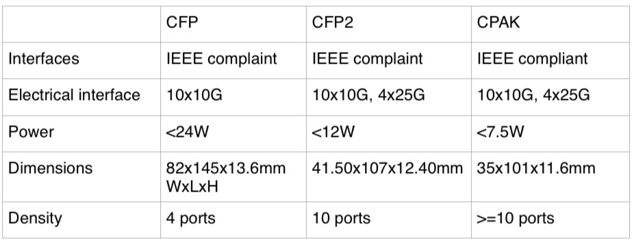
The CPAK module, smaller than the CFP2 MSA and three quarters its volume, has not been officially released and Cisco will not comment on the design but in certain company presentations the CPAK is compared with the CFP. The details are shown in the table above, with the CFP2’s details added.
The CPAK is the first example of Cisco's module design capability following its acquisition of silicon photonics player, Lightwire.
The development of the module highlights how the acquisition of core technology can give an equipment maker the ability to develop proprietary interfaces that promise costs savings and differentiation. But it also raises a question mark regarding the CFP2 and the merit of MSAs when a potential leading customer of the CFP2 chooses to use its own design.
 "The CFP2 has been a bit slow - the MSA has taken longer than people expected - so Cisco announcing CPAK has frightened a few people"
Paul Brooks, JDSU
Industry analysts do not believe it undermines the CFP2 MSA. “I believe there is business for the CFP2,” says Daryl Inniss, practice leader, Ovum Components. “Cisco is shooting for a solution that has some staying power. The CFP2 is too large and the power consumption too high while the CFP4 is too small and will take too long to get to market; CPAK is a great compromise.”
That said, Inniss, in a recent opinion piece entitled: Optical integration challenges component/OEM ecosystem, writes:
“Cisco’s Lightwire acquisition provides another potential attack on the traditional ecosystem. Lightwire provides unique silicon photonics based technology that can support low power consumption and high-density modules. Cisco may adopt a proprietary transceiver strategy to lower cost, decrease time to market, and build competitive barriers. It need not go through the standards process, which would enable its competitors and provide them with its technology. Cisco only needs to convince its customers that it has a robust supply chain and that it can support its product.”
Vladimir Kozlov, CEO of market research firm, LightCounting, is not surprised by the development. “Cisco could use more proprietary parts and technologies to compete with Huawei over the next decade,” he says. “From a transceiver vendor perspective, custom-made products are often more profitable than standard ones; unless Cisco will make everything in house, which is unlikely, it is not bad news.”
JDSU has just announced that its ONT-100G test set supports the CFP2 and CFP4. The equipment will also support CPAK. "We have designed a range of adaptors that allows us to interface to other optics including one very large equipment vendor's - Cisco's - own CFP2-like form factor," says Brooks.
However, Brooks still expects the industry to align on a small number of MSAs despite the advent of CPAK. "The majority view is that the CFP2 and CFP4 will address most people's needs," says Brooks. "Although there is some debate whether a QSFP2 may be more cost effective than the CFP4." The QSFP2 is the next-generation compact follow-on to the QSFP that supports the 4x25Gbps electrical interface.
The CFP2 pluggable module gains industry momentum
Finisar and Oclaro unveiled their first CFP2 optical transceiver products at the recent ECOC exhibition in Amsterdam. JDSU also announced that its ONT-100G test equipment now supports the latest 100Gbps module form factor.
 Source: Oclaro
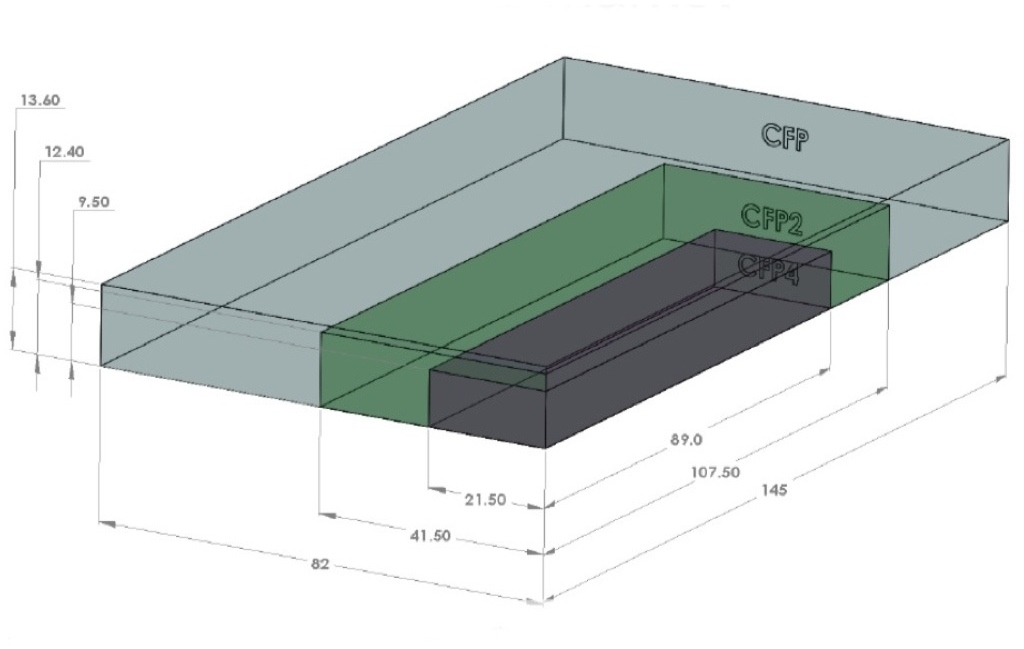
The CFP2 is the follow-on module to the CFP, supporting the IEEE 100 Gigabit Ethernet and ITU OTU4 standards. It is half the size of the CFP (see image) and typically consumes half the power. Equipment makers can increase the front-panel port density from four to eight by migrating to the CFP2.
Oclaro also announced a second-generation CFP supporting the 100GBASE-LR4 10km and OTU4 standards that reduces the power consumption from 24W to 16W. The power saving is achieved by replacing a two-chip silicon-germanium 'gearbox' IC with a single CMOS chip. The gearbox translates between the 10x10Gbps electrical interface and the 4x25Gbps signals interfacing to the optics.
The CFP2, in contrast, doesn’t include the gearbox IC.
"One of the advantages of the CFP2 module is we have a 4x25Gbps electrical interface," says Rafik Ward, vice president of marketing at Finisar. "That means that within the CFP2 module we can operate without the gearbox chip." The result is a compact, lower-power design, which is further improved by the use of optical integration.
"That 2.5x faster [interface of the CFP2] equates to about a 6x greater difficulty in signal integrity issues, microwave techniques etc"
Paul Brooks, JDSU
The transmission part of the CFP module typically comprises four externally modulated lasers (EMLs), each individually cooled. The four transmitter optical sub-assemblies (TOSAs) then interface to a four-channel optical multiplexer.
Finisar's CFP2 design uses a single TOSA holding four distributed feedback (DFB) lasers, a shared thermo-electric cooler and the multiplexer. The result of using DFBs and an integrated TOSA is that Finisar's CFP2 consumes just 8W.
Oclaro uses photonic integration on the receiver side, integrating four receiver optical sub-assemblies (ROSAs) as well as the optical demultiplexer into a single design, resulting in a 12W CFP2.
At ECOC, Oclaro demonstrated interoperability between its latest CFP and the CFP2. “It shows that the new modules will talk to existing ones,” says Robert Blum, director of product marketing for Oclaro's photonic components.
Meanwhile JDSU demonstrated its ONT-100G test set that supports the CFP2 and CFP4 MSAs.
"Initially the [test set] applications are focused on those doing the fundamental building blocks [for the 100G CFP2] – chip vendors, optical module vendors, printed circuit board developers," says Paul Brooks, director for JDSU's high speed transport test portfolio. "We will roll out more applications within the year that cover early deployment and production."
The standards-based client-side interfaces is an attractive market for test and measurement companies. For line-side optical transmission, much of the development work is proprietary such that developing a test set to serve vendors' proprietary solutions is not feasible.
The biggest engineering challenge for the CFP2 is its adoption of high-speed 25Gbps electrical interfaces. "The CFP was based on third generation, mature 10 Gig I/O [input/output]," says Brooks. "To get to cost-effective CFP2 [modules] is a very big jump: that 2.5x faster [interface] equates to about a 6x greater difficulty in signal integrity issues, microwave techniques etc."
The company says that what has been holding up the emergence of the CFP2 module has been the 104-pin connector: "The pluggable connector is the big headache," says Brooks. "The expectation is that very soon we should get some early connectors."
The test equipment also supports developers of the higher-density CFP4 module, and other form factors such as the QSFP2.
JDSU will start shipping its CFP2 test equipment in the first quarter of 2013.
Oclaro's second-generation CFP and the CFP2 transceivers are sampling, with volume production starting in early 2013.
Finisar's CFP2 LR4 product will sample in 2012 and enter volume production in 2013.