
Optical transport to grow at a 10% CAGR through 2017
- Global optical transport market to reach US $13bn in 2017
- 100 Gigabit to grow at a 75% CAGR
 "I won't be surprised if it [100 Gig] grows even faster"
Jimmy Yu, Dell'Oro Group
The Dell'Oro Group forecasts that the global optical transport market will grow to US $13 billion in 2017, equating to a 10-percent compound annual growth rate (CAGR).
In 2012 SONET/SDH sales declined by over 20 percent, greater than Dell'Oro expected, while wavelength-division multiplexing (WDM) equipment sales held their own.
Regions
Dell'Oro expects optical transport growth across all the main regions, with no one region dominating. The market research company does foresee greater growth in Europe given the prolonged underspend of recent years.
European operators are planning broadband access investment such as fibre-to-the-cabinet/ VDSL vectoring as well as fibre-to-the-home. "That will drive demand for backhaul bandwidth and that is where WDM fits in well," says Jimmy Yu, vice president, microwave transmission, mobile backhaul and optical transport at Dell'Oro.
Technologies
Forty and 100 Gigabit optical transport will be the main WDM growth areas through 2017. Yu expects 40 Gigabit demand to grow over the forecast period even if the growth rate will taper off due to demand for 100 Gigabit.
The 100 Gigabit market continues to exceed Dell'Oro's forecasted growth. The market research company predicts 100-Gbps wavelength shipments to grow at a 75 percent CAGR over the next five years, accounting for 60 percent of the WDM capacity shipments by 2017. "I won't be surprised if it [100 Gig] grows even faster," says Yu.
"A lot of people wonder why have 40 Gig when there is 100 Gig? But that granularity does help service providers; having 40 Gig and 100 Gig rather than going straight from 10 Gig to 100 Gig," says Yu. The 100 Gig sales span metro and long-haul networks with the latter generating greater revenue due to the systems being pricier. "Forty Gigabit sales were predominantly long haul originally but we are seeing a good chunk of growth in metro as well," says Yu.
The current forecast does not include 400Gbps optical transport sales though Yu does expect sales to start in 2016.
Dell'Oro is seeing sales of 100 Gigabit direct detection but says it will remain a niche market. "We are talking tens of [shipped] units a quarter," says Yu.
There are applications where customers will need links of 80km or several hundred kilometers and will want the lowest cost solution, says Yu: "There is a market for direct detection; it will not be a significant driver for 100 Gig but it will be there."
Achieving 56 Gigabit VCSELs
A Q&A with Finisar's Jim Tatum, director of new product development. Tatum talks about the merits of the vertical-cavity surface-emitting laser (VCSEL) and the challenges to get VCSELs to work at 56 Gigabit.
Briefing: VCSELs
 VCSELs galore! A wafer of 28 Gig devices Source: Finisar
Q. What are the merits of VCSELs compared to other laser technologies?
A: VCSELs have been a workhorse for the datacom industry for some 15 years. In that time there have been some 500 million devices deployed for data infrastructure links, with Finisar being a major producer of these VCSELs.
The competition is copper which means you need to be at a cost that makes such [optical] links attractive. This is where VCSELs have value: operating at 850nm which means running on multi-mode fibre.
Coupling VCSELs to multi-mode fibre [the core diameter] is in the tens of microns whereas it is one micron for single-mode fibre and that is where the cost is. Also with VCSELs and multi-mode fibre, we don't need optical isolators which add significant cost to the assemblies. It is not the cost of the laser die itself; the difference in terms of the link [approaches] is the cost of the optics and getting light in and out of the fibre.
There are also advantages to the VCSEL itself: wafer-level testing that allows rapid testing of the die before you commit to further packaging costs. This becomes more important as the VCSEL speed gets higher.
What are the differences with 850nm VCSELs compared to longer wavelength (1300nm and 1550nm) VCSELs?
At 850nm you are growing devices that are all epitaxial - the laser mirrors are grown epitaxially and the quantum wells are grown in one shot. At the other wavelengths, it is much harder.
People have managed it at 1300nm but it is not yet proven to be a reliable material system for getting high-speed operation. When you go to 1550nm, you are doing wafer bonding of the mirrors and active regions or you are doing more complex epitaxial processing.
That is where 850nm VCSELs has a nice advantage in that the whole thing is done in one shot; the epitaxy and the fabrication are relatively simple. You don't have the complex manufacturing of chip parts that you do at 1550nm.
What link distances are served by 850nm VCSELs?
The longest standards are for 500m. As we venture to higher speeds - 28 Gigabit-per-second (Gbps) - 100m is more the maximum. And this trend will continue, at 56Gbps I would anticipate less than 50m and maybe 25m.
The good news is that the number of links that become economically viable at those speeds grows exponentially at these shorter distances. Put another way, copper is very challenged at 56Gbps lane rates and we'll see optics and VCSEL technology move inside the chassis for board-to-board and even chip-to-chip interconnects. Such applications will deliver much higher volumes.
"Taking that next step - turning the 28Gbps VCSEL into a product - is where all the traps lie"
What are the shortest distances?
There are the edge-mounted connections and those are typically 1-5m. There is also a lot of demonstrated work with VCSELs on boards doing chip-to-chip interconnect. That is a big potential market for these devices as well.
The 28Gbps VCSEL has been demonstrated but commercial products are not yet available. It is difficult to sense whether such a device is relatively straightforward to develop or a challenge.
Achieving a 28Gbps VCSEL is hard. Certainly there have been many companies that have demonstrated a modulation capability at that speed. However, it is one thing to do it one time, another to put a reliable VCSEL product into a transceiver with everything around it.
Taking that next step - turning the 28Gbps VCSEL into a product - is where all the traps lie. That is where the bulk of the work is being done today. Certainly this year there will be 25Gbps/ 28Gbps products out in customers' hands.
"With a VCSEL, you have to fill up a volume of active region with enough carriers to generate photons and you can only put in so many, so fast. The smaller you can make that volume, the faster you can lase."
What are the issues that dictate a VCSEL's speed?
When you think about going to the next VCSEL speed, it helps to think about where we came from.
All the devices shipped, from 1 to 10 Gig, had gallium arsenide active regions. It has lots of wonderful attributes but one of its less favourable ones is that it is not the highest speed. Going to 14Gbps and 28Gbps we had to change the active region from gallium arsenide to indium gallium arsenide and that gives us an enhancement of the differential gain, a key parameter for controlling speed.
What you really want to do when you are dealing with speed is that for every incremental bit of current I give the [VCSEL] device, how much more does that translate into gain, or more photons coming out? If you can make that happen more efficiently, then the edge speed of the device increases. In other words, you don't have to deal with other parasitics - carriers going into non-recombination centres and that sort of thing; everything is going into the production of photons rather than other parasitic things.
With a VCSEL, you have to fill up a volume of active region with enough carriers to generate photons and you can only put in so many, so fast. The smaller you can make that volume, the faster you can lase.
Differential gain is a measure of the efficiency in terms of the number of photons generated by a particular carrier. If I can increase that efficiency of making photons, then my transition speed and my edge speed of the laser increases.

Shown is the chart on the y-axis is the differential gain and on the x-axis is the current density going into the part. The decay tells you that if I'm running really high currents, the differential gain is worse for indium gallium arsenide parts. So you want to operate your device with a carrier density that maximises the differential gain.
Part of that maximisation is using less carriers in smaller quantum wells so that it ramps up the curve. You want to operate at a lower current density while also doing a better job of each carrier transitioning into photons.
What else besides differential gain dictates VCSEL performance?
The speed of the laser increases above threshold as the square root of the current. That gives you a return-on-investment in terms of how much current you put into the device.
However, the reliability of the part degrades with the cube of the current you put into it. So you get to a boundary condition where speed varies as the square root of the current and you have the reliability which is degrading with the cube of the current. The intersection of those two points is where you are willing to live in terms of reliability.
That is the trade-off we constantly have to deal with when designing lasers for high speed communications.
Having explained the importance of this region of operation, what changes in terms of the laser when operating at 28Gbps and at 56Gbps?
At 14Gbps and even at 28Gbps the lasers are directly modulated with little analogue trickery. That said, 28Gbps Fibre Channel does allow you to use equalisation at the receiver.
My feeling today is that at 56Gbps, direct modulation of the laser is going to be pretty tricky. At that speed there is going to have to be dispersion compensation or equalisation built into the optical system.
There are a lot of ways to incorporate some analogue or even digital methods to reduce the effective bandwidth of the device from 56Gbps to running less. One of these is a little bit of pre-emphasis and equalisation. Another way is to use analogue modulation levels. Alternatively, you can start borrowing a whole lot more from the digital communication world and look at sub-carrier multiplexing or other more advanced modulation schemes. In other words pull the bandwidth of the laser down instead of doing 1, 0 on-off stuff. At 56 Gig those things are going to be a requirement.
The bottom line is that a 28Gbps VCSEL design maybe something pretty similar to a 56 Gig part with the addition of bandwidth enhancements techniques.
"I can see [VCSEL] modulation rates going to 100Gbps"
So has VCSEL technology already reached its peak?
In terms of direct modulation of a VCSEL - pushing current into it and generating photons - 28 Gig is a reasonable place. And 56 Gig or 40Gig VCSELs may happen with some electronic trickery around it.
The next step - and even at 56Gbps - there is a fair amount of investigation of alternate modulation techniques for VCSELs.
Instead of modulating the current in the active region, you can do passive modulation of an external absorber inside the epitaxial structure. That starts to look like a modulated laser you would see in the telecom industry but it is all grown expitaxially. Once you are modulating a passive component, the modulation speed can get significantly higher. I can see modulation rates going to 100Gbps, for example.
The VCSEL roadmap isn't running out then, but it is getting more complicated. Will it take longer to achieve each device transition: from 28 to 56Gbps, and from 56Gbps to 112Gbps?
A question that is difficult to answer.
The time line will probably scale out every time you try to scale the bandwidth. But maybe not if you are able to do things like combine other technologies at 56Gbps or you do things that are more package related. For example, one way to achieve a 56 Gig link is to multiplex two lasers together on a multi-core fibre. That is significantly less challenging thing to do from a technology development point of view than lasers fundamentally capable of 56Gbps. Is such a solution cost optimised? Well, it is hard to say at this point but it may be time-to-market optimised, at least for the first generation.
Multi-core fibre is one way, another is spatial-division multiplexing. In other words, coarse WDM, making lasers at 850nm, 980nm, 1040nm - a whole bunch of different colours and multiplexing them.
There is more than one way to achieve a total aggregate throughput.
Does all this make your job more interesting, more stressful, or both?
It means I have options in my job which is always a good thing.
Optical transceiver market to grow 50 percent by 2017
- The optical transceiver market will grow to US $5.1bn in 2017
- The fierce price declines of 2012 will lessen during the forecast period
- Stronger traffic growth could have a significant positive effect on transceiver market growth
 "The price declines in 2012 were brutal but they will not happen again [during the forecast period]"
Vladimir Kozlov, LightCounting
The global optical transceiver market will grow strongly over the next five year to $5.1bn in 2017, from $3.4bn in 2012. So claims market research company, LightCounting, in its latest telecom and datacom forecast.
"That [market value] does not include tunable lasers, wavelength-selective switches, pump lasers and amplifiers which will add some $1bn or $2bn more [in 2017]," says Vladimir Kozlov, CEO of LightCounting.
One key assumption underpinning the forecast is that competitive pressures will ease. "The price declines in 2012 were brutal but they will not happen again [during the forecast period]," says Kozlov.
Optical transceivers
The optical transceiver market saw price declines as high as 30 percent last year. These were not new products ramping in volume where sharp price declines are to be expected, says Kozlov. Last year also saw fierce competition among the service providers while the steepest price declines were experienced by the telecom equipment makers.
One optical transceiver sector that performed well last year is high-speed optical transceivers and in particular Ethernet.
The 100 Gigabit Ethernet (GbE) market saw revenue growth due to strong demand for the 100GBASE-LR4 10km transceiver even though its unit price declined 30 percent. This is a sector the Chinese optical transceiver players are eyeing as they look to broaden the markets they address.
One unheralded market that did well was 40 Gigabit transceivers for telecoms and the data centre. "This is 40 Gig short reach mostly - up to 100m - but also 10km reach transceivers did well in the data centre," says Kozlov.
LightCounting expects the steady growth of 40GbE to continue; 40GbE transceivers use 10 Gig technology co-packaged into one module, offer improved port density and have a lower power and cost compared to four 10GbE transceivers.
Even the veteran 10GbE market continues to grow. Some 7-8M 10GbE short reach and long reach units were sold in 2012 growing to 10M units this year.
Meanwhile, the 100 Gigabit coherent long-haul transponder market was small in 2012. The optical vendors only started selling in volume last year and most of the system vendors manufacture their own 100 Gigabit-per-second (Gbps) designs using discrete components. "Those companies that sell modulators and receivers for 100 Gig did really well in 2012," says Kozlov.
LightCounting expects the 100Gbps coherent transponder market will grow in 2013 as system vendors embrace more third-party 100 Gig transponders. "We estimate that the optical transceiver vendors captured 10-15 percent of the 40 and 100 Gig market and this will grow to 18-20 percent in 2013," says Kozlov.
Other markets that grew in 2012 include optical access. The fibre-to-the-x (FTTx) continues to grow in terms of units shipped, with transceivers and board optical sub-assembly (BOSA) designs sharing the volumes.
LightCounting says that the number of optical network units (ONU) exceeded by more than double the number of FTTx subscribers added in 2012: 35-40M ONU transceivers and BOSAs compared to 15M new subscribers.
The result was a market value of $700M in 2012 compared to $300M in 2009. But because of the excess in shipments compared to new subscribers, Kozlov expects the FTTx market to slow down. "That is probably a sure sign that it is going to grow again," he quips.
Market expectations
Kozlov will be watching how the optical interconnect market does this year. The active optical cable market did well in 2012 and this is likely to continue. Kozlov is interested to see if silicon photonics starts to make its mark in the transceiver market, citing as an example Cisco's in-house silicon photonics-based CPAK transceiver. He also expects the 40G and 100Gbps module makers to do well.
LightCounting stresses the wide discrepancy between video traffic growth through 2017 as forecast by Bell Labs and by Cisco Systems. This is important because the optical transceiver forecast model developed by LightCounting is sensitive to traffic growth. LightCounting has averaged the two forecasts but if video traffic grows more quickly, the overall transceiver market will exceed the market research company's 2017 forecast.
Another reason why Kozlov is upbeat about the market's prospects is that while the system vendors suffered the sharpest price declines - up to 35 percent in 2012 - this will not continue.
The sharp falls in equipment prices were due largely to the fierce competition provided by the Chinese giants Huawei and ZTE. But relief is expected with government initiatives in Europe and the United States to limit the influence of Huawei and ZTE, says Kozlov.
The U.S. government has effectively restricted sales of Huawei and ZTE networking equipment to major U.S. carriers due to cyber security concerns, while the European Commission has determined that Huawei and ZTE are both inflicting damage on European equipment vendors by dumping products onto the European market.
EZchip expands the role of the network processor
- EZchip's NPS-400 will be a 200Gbps duplex chip capable of layer 2 to layer 7 network processing
- The device is being aimed at edge routers and the data centre
- First samples by year end
EZchip Semiconductor has announced a class of network processor capable of performing traditional data plane processing as well as higher layer networking tasks. EZchip's announced NPS will extend the role of the network processor to encompass layer two to layer seven of the network. Source: EZchip
"It [the device family] is designed to provide processing for all the networking layers, from layer two all the way to layer seven," says Amir Eyal, EZchip’s vice president of business development. Network processors typically offer layer-two and layer-three processing only.
The device family, called the network processor for smart networks (NPS), is being aimed at Carrier Ethernet edge router platforms, the traditional telecom application for network processors.
But the NPS opens up new opportunities for EZchip in the data centre, such as security, load balancing and software-defined networking (SDN). Indeed EZchip says the NPS market will double the total addressable market to US$2.4bn by 2016.
"SDN is supposedly a big deal in the data centre," says Eyal. Because SDN separates the control plane from the data plane, it implies that the data plane becomes relatively simple. In practice the opposite is true: the data processing becomes more complex requiring the recognition and handling of packets having different encapsulation schemes, says Eyal.
The NPS borrows architectural elements of EZchip's existing high-end NPUs but the company has added an ARC 32-bit reduced instruction set computer (RISC) processor which it has redesigned to create the basic packet-processing computing node: the CTOP (C-programmable task-optimised processor).
EZchip has announced two NPS devices: The NPS-200 and the more processing-capable NPS-400. The NPS-400 is a 200 Gigabit-per-second (Gbps) duplex chip with 256 CTOPs, giving it twice the packet-processing performance of EZchip's latest NP-5 NPU. The NPS-400 will also have 800 Gigabit of input/ output. The NPS-200 design will have 128 CTOPs.
As a result of adding the ARC, the NPS family will be C-programmable whereas NPUs are programmed using assembly language or micro-code. The CTOP will also be able to processes 16 instruction threads whereas the standard ARC is single thread.
The NPS also features an on-chip traffic manager which controls the scheduling of traffic after it has been processed and classified.
The power consumption of the NPS has yet to be detailed but Eyal says it will be of the order of the NP-5 which is 60W.
EZchip says up to eight NPS chips could be put on a line card, to achieve a 1.6Tbps packet throughput, power-consumption permitting.
Adopting the NPS processor will eliminate the need to add to platforms service line cards that use general-purpose processors. More NPS-based cards can then be used in the vacated line-card slots to boost the platform's overall packet-processing performance.
The company started the NPS design two years ago and expects first samples at the end of 2013. NPS-based products are expected to be deployed in 2015.
Meanwhile, EZchip says it is sampling its NP-5 NPU this quarter. The NPS will overlap with the NP-5 and be available before the NP-6, the next NPU on EZchip's roadmap.
Will the NPS-400 with double the throughput not deter sales of the NP-5, even if the design is used solely for traditional NPU layer-two and layer-three tasks?
EZchip says new customers will likely adopt the NPS especially given its support for high-level programming. But existing customers using the NP-4 will prefer to stay with the NPU family due to the investment already made in software.
Further reading:
Microprocessor Report: EZchip breaks the NPU mold, click here
A Terabit network processor by 2015?, click here
A FOX-C approach to flexible optical switching
Flexible switching of high-capacity traffic carried over ’super-channel' dense-wavelength division multiplexing wavelengths is the goal of the European Commission Seventh Framework Programme (FP7) research project.
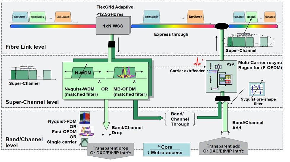
The €3.6M FOX-C (Flexible optical cross-connect nodes) will develop a flexible spectrum reconfigurable optical add/drop multiplexer (ROADM) for 400Gbps and one Terabit optical transmission. The ROADM will be designed not only to switch super-channels but also the carrier constituent components.
Companies involved in the project include operator France Telecom and optical component player Finisar. However, no major European system vendor is taking part in the FOX-C project although W-Onesys, a small system vendor from Spain, is participating.
 “We want to transfer to the optical layer the switching capability”
Erwan Pincemin, FT-Orange
“It is becoming more difficult to increase the spectral efficiency of such networks,” says Erwan Pincemin, senior expert in fibre optic transmission at France Telecom-Orange. “We want to increase the advantages of the network by adding flexibility in the management of the wavelengths in order to adapt the network as services evolve.”
FOX-C will increase the data rate carried by each wavelength to achieve a moderate increase in spectral efficiency. Pincemin says such modulation schemes as orthogonal frequency division multiplexing (OFDM) and Nyquist WDM will be explored. But the main goal is to develop flexible switching based on an energy efficient and cost effective ROADM design.
The ROADM’s filtering will be able to add and drop 10 and 100 Gigabit sub-channels or 400 Gigabit and 1 Terabit super-channels. By using the developed filter to switch optically at speeds as low as 10 Gigabit, the aim is to avoid having to do the switching electrically with its associated cost and power consumption overhead. “We want to transfer to the optical layer the switching capability,” says Pincemin.
While the ROADM design is part of the project’s goals, what is already envisaged is a two-stage pass-through-and-select architecture. The first stage, for coarse switching, will process the super-channels and will be followed by finer filtering to extract (drop) and insert (add) individual lower-rate tributaries.
The project started in Oct 2012 and will span three years. The resulting system testing will take place at France-Telecom Orange's Lab in Lannion, France.
Project players
The project’s technical leader is the Athens Institute of Technology (AIT), headed by Prof. Ioannis Tomkos, while the administrator leader is the Greek company Optronics Technologies.
Finisar will provide the two-stage optical switch while France Telecom-Orange will test the resulting ROADM and will build the multi-band OFDM transmitter and receiver to evaluate the design.
Athens Institute of Technology will work with Finisar on the technical aspects and in particular a flexible networking architecture study. The Hebrew University is working with Finisar on the design and the building of the ultra-selective adaptive optical filter, and has expertise is free-space optical systems. The Spanish firm, W-Onesys, is a system integration specialist and will also work with Finisar to integrate its wavelength-selective switch for the ROADM. Other project players include Aston University, Tyndall National Institute and the Karlsruhe Institute of Technology.
No major European system vendor is taking part in the FOX-C project. According to Pincemin this is regrettable although he points out that the equipment players are involved in other EC FP7 projects addressing flexible networking.
He believes that their priorities are elsewhere and that the FOX-C project may be deemed as too forward looking and risky. “They want to have a clear return on investment on their research,” says Pincemin.
PCIe 3.0 and USB 3.0 to link mobile chip
- Both protocols to run on the MIPI Alliance's M-PHY transceiver
- Goal is to exploit existing PCIe and USB driver and application software while benefitting from the low power M-PHY
- OcuLink cable based on PCIe 3.0 promises up to 32 Gigabit
 Source: Gazzetabyte
At first glance the Peripheral Component Interconnect Express (PCIe) bus has little in common with the Universal Serial Bus (USB) interface.
PCIe is a multi-lane bus standard used to move heavy data payloads over computing backplanes while USB is a consumer electronics interface. Yet certain areas of overlap are appearing.
The PCI Special Interest Group (PCI-SIG) is looking to get PCIe adopted within mobile devices - tablets and smartphones - for chip-to-chip communication, an application already performed by the 480Mbps USB 2.0 High-Speed Inter-Chip (HSIC) standard.
PCI-SIG is also developing the OcuLink external copper cable for storage and consumer applications.
PCIe is a point-to-point link that can also be switched, and is used to connect processors, processors to co-processors and for storage. Now, USB 3.0 and PCIe 3.0 are set to play an embedded role within mobile devices.
Handsets use the Mobile Industry Processor Interface (MIPI) Alliance's interfaces centred on the handset's mobile application processor, with several MIPI point-to-point interfaces defined to link to the handset's baseband processor, display and camera sensor.
Two physical (PHY) devices - D-PHY or the M-PHY - are used by MIPI. The M-PHY is the faster of the two (up to 5.8Git/s compared to the D-PHY's 1Gbit/s). It is the M-PHY transceiver that is used in links between the handset’s application processor to the radio, display and camera sensor. And it is the M-PHY that will run the USB 3.0-based SuperSpeed InterChip (SSIC) - the follow-on to HSIC - and PCIe 3.0.
The motivation is to benefit from the huge amount of software drivers and applications developed for USB and PCIe, while taking advantage of M-PHY's lower power consumption than the USB's or PCIe's own transceivers.
M-PHY runs at 1.25-1.45Gbps while two faster versions are in development: 2.5-2.9Gbps and up to 5.8Gbps.
A PHY adaptor layer, known as the PIPE 3.0-to-M-PHY bridge, translates the USB protocol onto M-PHY. The same strategy is being pursued by the PCI-SIG using a logical PHY to run PCIe 3.0 on M-PHY.
The PCI-SIG group hopes to have the PCIe 3.0 mobile specification completed in the first quarter of 2013.
Meanwhile, the OcuLink cable will initially be a copper cable interface designed as a compact, low cost interface that will support one, two and four lanes of PCIe 3.0. Two versions are planned: a passive and an active copper cable before a fibre-based version will be developed.
Uses of OcuLink will include connecting to storage devices and to audiovisual equipment.
A more detailed article on PCIe and USB for mobile will appear in an upcoming article for New Electronics
Transmode's evolving packet optical technology mix
- Transmode adds MPLS-TP, Carrier Ethernet 2.0 and OTN
- The three protocols make packet transport more mesh-like and service-aware
- The 'native' in Native Packet Optical 2.0 refers to native Ethernet
Transmode has enhanced its metro and regional network equipment to address the operators' need for more efficient and cost-effective packet transport.

“Native Packet Optical 2.0 extends what the infrastructure can do, with operators having the option to use MPLS-TP, Carrier Ethernet 2.0 and OTN, making the network much more service-aware”
Jon Baldry, Transmode
Three new technologies have been added to create what Transmode calls Native Packet Optical 2.0 (NPO2.0). Multiprotocol Label Switching - Transport Profile (MPLS-TP) was launched in June 2012 to which has now been added the Metro Ethernet Forum's (MEF) latest Carrier Ethernet 2.0 (CE2.0) standard. The company will also have line cards that support Optical Transport Network (OTN) functionality from April 2013.
Until several years ago operators had distinct layer 2 and layer 1 networks. “The first stage of the evolution was to collapse those two layers together,” says Jon Baldry, technical marketing director at Transmode. “NPO2.0 extends what the infrastructure can do, with operators having the option to use MPLS-TP, CE2.0 and OTN, making the network much more service-aware.”
By adopting the enhanced capabilities of NPO2.0, operators can use the same network for multiple services. “A ROADM based optical layer with native packet optical at the wavelength layer,” says Baldry. “That could be a switched video distribution network or a mobile backhaul network; doing many different things but all based on the same stuff.”
Transmode uses native Ethernet in the metro and OTN for efficient traffic aggregation. “We are using native Ethernet frames as the payload in the metro,” says Baldry. “A 10 Gig LAN PHY frame that is moved from node to node, once it is aggregated from Gigabit Ethernet to 10 Gig Ethernet; we are not doing Ethernet over SONET/SDH or Ethernet over OTN.”
![]() Shown are the options as to how layer 2 services can be transported and interfaced to multiple core networks. The Ethernet muxponder supports MPLS-TP, native Ethernet and the option for OTN, all over a ROADM-based optical layer. “It is not just a case of interfacing to three core network types, we can be aware of what is going on in these networks and switch traffic between types,” says Transmode's Jon Baldry. Note: EXMP is the Ethernet muxponder. Source: Transmode.
Shown are the options as to how layer 2 services can be transported and interfaced to multiple core networks. The Ethernet muxponder supports MPLS-TP, native Ethernet and the option for OTN, all over a ROADM-based optical layer. “It is not just a case of interfacing to three core network types, we can be aware of what is going on in these networks and switch traffic between types,” says Transmode's Jon Baldry. Note: EXMP is the Ethernet muxponder. Source: Transmode.
Once the operator no longer needs to touch the Ethernet traffic, it is then wrapped in an OTN frame for aggregation and transport. This, says Baldry, means that unnecessary wrapping and unwrapping of OTN frames is avoided, with OTN being used only where needed.
There are economical advantages in adopting NPO2.0 for an operator delivering layer 2 services. There are also considerable operational advantages in terms of the way the network can be run using MPLS-TP, the service types offered with CE2.0, and how the metro network interworks with the core network, says Baldry.
MPLS-TP and Carrier Ethernet 2.0
Introducing MPLS-TP and the latest CE2.0 standard benefits transport and services in several ways, says Baldry.
MPLS-TP provides better traffic engineering as well as working practices similar to SONET/SDH that operators are familiar with. “MPLS-TP creates a transport-like way of dealing with Ethernet which is good for operators having to move from a layer-1-only world to a packet world,” says Baldry. MPLS-TP is also claimed to have a lower total cost of ownership compared to IP/MPLS when used in the metro.
The protocol is also more suited to the underlying infrastructure. “Quite a lot of the networks we are deploying have MPLS-TP running on top of a ROADM network, which is naturally mesh-like,” says Baldry.
In contrast Ethernet provides mainly point-to-point and ring-based network protection mechanisms; there is no support for mesh-based restoration. This resiliency option is supported by MPLS-TP with its support of mesh-styled ‘tunnelling’. A MPLS-TP tunnel creates a service layer path over which traffic is sent.
“You can build tunnels and restoration paths through a network in a way that is more suited to the underlying [ROADM-based] infrastructure, thereby adding resiliency when a fibre cut occurs,” says Baldry.
MPLS-TP also benefits service scalability. It is much easier to create a tunnel and its protection scheme and define the services at the end points than to create many individual circuits across the network, each time defining the route and the protection scheme.
“Because MPLS-TP is software-based, we can mix and match MPLS-TP and Ethernet on any port,” says Baldry. “You can use MPLS-TP as much or as little as you like over particular parts of the network.”
The second new technology, the MEF’s Carrier Ethernet 2.0, benefits services. The MEF has extended the range of services available, from three to eight with CE2.0, while improving class-of-service handling and management features.
Transmode says its equipment is CE2.0 compliant and suggests its systems will become CE2.0-certified in the new year.
Hardware
The packet-optical products of Transmode comprise the TM-Series transport platforms and Ethernet demarcation units.
The company's single and double slot cards - Ethernet muxponders – fit into the TM-Series transport platforms. The single-slot Ethernet muxponder has ten, 1 Gigabit Ethernet (GbE) and 2x10GbE interfaces while the double-slot card supports 22, 1GbE and 2x10GbE interfaces. Transmode also offers 10GbE only cards: the single slot is 4x10GbE and the double-slot has 8x10GbE interfaces. These cards are software upgradable to support MPLS-TP and the MEF’s CE2.0.
“In early 2013, we are introducing a couple of new cards – enhanced Ethernet muxponders – with more gutsy processors and optional hardware support for OTN on 10 Gigabit lines,” says Baldry.
The Ethernet demarcation unit, also known as a network interface device (NID), is a relatively small unit that resides for example at a cell site. The unit undertakes such tasks as defining an Ethernet service and performance monitoring. The box or rack mounted units have Gigabit Ethernet uplinks and interface to Transmode’s platforms.
Baldry cites the UK mobile operator, Virgin Media, which is using its platforms for mobile backhaul. Here, the Ethernet demarcation units reside at the cell sites, and at the first aggregation point the10- or 22-port GbE card is used. These Ethernet muxponder cards then feed 10GbE pipes to the 4- or 8-port 10GbE cards.
“For the first few thousand cell sites there are hundreds of these aggregation points,” says Baldry. “And those aggregation points go back to Virgin Media’s 50-odd main sites and it is at those points we put the 8x 10GbE cards.” Thus the traffic is backhauled from the edge of the network and aggregated before being handed over as a 10GbE circuit to Virgin Media’s various radio network controller (RNC) sites.
Transmode says that half of it customers use its existing native packet optical cards in their networks. Since MPLS-TP and CE2.0 are software options, these customers can embrace these features once they are required.
However, operators will only likely start deploying CE2.0-based services once Transmode’s offering becomes certified.
Further reading:
Detailed NPO2.0 application note, click here
ECI Telecom’s next-generation metro packet transport family
- The Native Packet Transport (NPT) family targets the cost-conscious metro network
- Supports Ethernet, MPLS-TP and TDM
- ECI claims a 65% lower total cost of ownership using MPLS-TP and native TDM
 NPT's positioning as part of the overall network. Source: ECI Telecom
ECI Telecom has announced a product line for packet transport in the metro. The Native Packet Transport (NPT) family aims to reduce the cost of operating packet networks while supporting traditional time division multiplexing (TDM) traffic.
“Eventually, in terms of market segments, it [NPT] is going to replace the multi-service provisioning platform,” says Gil Epshtein, product market manager at ECI Telecom. “The metro is moving to packet and so it is moving to new equipment to support this shift.”
The NPT is ECI’s latest optimised multi-layer transport (OMLT) architecture, and is the feeder or aggregator platform to the optical backbone, addressed by the company's Apollo OMLT product family announced in 2011.
 “The whole point of shifting to packet is to lower the [transport] cost-per-bit”
Gil Epshtein, ECI Telecom
Packet transport issues
“Building carrier-grade packet transport is proving more costly than anticipated,” says Epshtein. “Yet the whole point of shifting to packet is to lower the [transport] cost-per-bit.”
Several packet control plane schemes can be used for the metro, a network that can be divided further into the metro core and metro access/ aggregation. The two metro segments can use either IP/MPLS (Internet Protocol/ Multiprotocol Label Switching) or MPLS-TP (Multiprotocol Label Switching Transport Profile). Alternatively, the two metro segments can use different schemes: the metro core IP/MPLS and metro access MPLS-TP, or MPLS-TP for the core and Ethernet for metro access.
Based on total cost of ownership (TCO) analysis, ECI argues that the most cost-effective packet control plane scheme is MPLS-TP. “The NPT product line is based on MPLS-TP, designed to simplify and make MPLS affordable for transport networks,” says Epshtein.
Three issues contribute to the cost of building and operating packet-based transport. The first is capital expenditure (capex) – the cost of the equipment and what is needed to make the network carrier grade such as redundancy and availability.
The second is operational expenditure or opex. Factors include the training and expertise needed by the staff, and their number and salaries. In turn, issues such as network availability, equipment footprint and the power consumption requirements.
“More and more operators view opex as a key factor in their TCO considerations,” says Epshtein. Operators look at the entire network and want to know what its cost of operation will be.
A third cost factor is the existence of both TDM and packet data in the operators’ networks. “When you look at the overall TCO, you need to take this into consideration,” says Epshtein. For some operators it [TDM] is more significant but it is always there, he says.
The NPT family is being aimed at various customers. One is operators that want to extend MPLS from the core to the metro network. “Here, TDM is not a factor,” says Epshtein. “We find this in wireless backhaul, in triple-play, carriers-of-carriers and business applications.” The second class of operators is those with legacy TDM traffic. Also being targeted are utilities. “Here reliability and security are key.”
Analysis
The choice of packet control plane - whether to use IP/MPLS or MPLS-TP - impacts both capex and opex. How the TDM traffic is handled, whether using circuit emulation over packets or native TDM, also impacts overall costs.
According to ECI, the number of network elements grows some tenfold with each segment transition towards the network edge. In the network core there are 100s of network elements, 1000s in the metro core and 10,000s in the metro access. The choice of packet control plane for these network elements clearly impacts the overall cost, especially in the cost-conscious metro as the number of platforms grows. “A network element based on MPLS-TP is lower cost than IP/MPLS,” says Epshtein. “The main reason being it is a lot less complex.”
He stresses that MPLS-TP is not a competing standard to IP/MPLS; IP/MPLS is the defacto standard in the network core. Rather, MPLS-TP is a derivative designed for transport. The debate here, says Epshtein, is what is best for metro.
“The main difference between the two standards is the control plane, not the data plane,” says Epshtein. MPLS-TP removes unnecessary control plane functions supported by IP/MPLS leading to simpler metro platform functionality, and simpler management and operation of the equipment. “We believe MPLS-TP is more suited to the metro due to its simplicity, scalability and capex benefits.”
Working with market research company, ACG Research, the TCO analysis (opex and capex) over five years using MPLS-TP was 55% lower than using IP/MPLS for metro packet transport (with no TDM traffic).
The cost savings was even greater with both packet and some TDM traffic.
Using the NPT, capex goes up 5% due to the line cards needed to support native TDM traffic. But for IP/MPLS using circuit emulation capex increases 37%, resulting in the NPT having a 66% lower capex overall. The resulting opex is also 64% lower. Overall TCO is lowered by 65% using MPLS-TP and native TDM compared to IP/MPLS and circuit emulation.
NPT portfolio
ECI says its NPT supports circuit emulation and native TDM. Having circuit emulation enables the network to converge to packet only. But native TDM simplifies the interfacing to legacy networks and also has lower latency than circuit emulation.
 The NPT packet switch and TDM switch fabrics and the traffic types carried over each. Source: ECI Telecom
There are five NPT platforms ranging from the NPT-1020 for metro access to the NPT-1800 for the metro core. The NPT-1020 has a 10 or 50 Gigabit packet switch capacity option and a TDM capacity of 2.5 Gigabit. The NPT-1800 has a packet switching capacity of 320 or 640 Gigabit and 120 Gigabit for TDM.
The metro aggregation NPT-1600 and 1600c (160 Gig packet/120 Gig TDM capacity) platforms are available now. The remaining platforms will be available in the first half of 2013.
ECI says it has already completed several trials with existing and new customers. "We have already won a few deals," says Epshtein.
The platforms are managed using ECI’s LightSoft software, the same network management system used for the Apollo. ECI has added software specifically for packet transport including service provisioning, performance management and troubleshooting.
Further information, click here.
Carrier Ethernet switch chip for wireless small cells
- 6-port low power 12 Gigabit Carrier Ethernet switch chip
- Used for intra and inter-board comms, and back-hauling
- Supports MPLS and MPLS-TP

"Multi-carrier OA&M performance monitoring allows you to manage your network for your users through another carrier’s network”
Uday Mudoi, Vitesse Semiconductor
Vitesse Semiconductor has launched an Ethernet switch chip for Long Term Evolution (LTE) small cells.
Small cells are being adopted by mobile operators as a complement to their existing macrocells to boost signal coverage and network capacity. The small cells include microcells and picocells as well as femtocells for the enterprise.
The Serval Lite chip, the VSC7416, from Vitesse will be used to aggregate and switch traffic and will reside at the interface between the access and the pre-aggregation segments of the mobile network.
According to Uday Mudoi, director of product marketing at Vitesse, two units make up a carrier’s small cell: the base station and the back-hauling. The base station itself comprises baseband and general purpose processing. “What we are seeing on a base station – whether it is a macro or a small cell – is the use of multi-core processors, and you may need more than one such device on the baseband card,” says Mudoi. The Serval Lite IC can be used as an interface between the baseband and general purpose processors, and to other hardware on the card.
 The basestation features baseband (BB) and general purpose processing (GPP) cards. Source: Vitesse
The backhaul unit also features the Serval Lite IC. “The backhaul is more interesting from a switch perspective,” says Mudoi. The switch takes traffic from the base stations and places it on the outgoing interface, typically a microwave or fibre link, says Mudoi.
The switch also supports Carrier Ethernet for the traffic back-hauling. Such features include hierarchical quality of service (QoS), performance monitoring and operations, administration and management (OA&M). "Multi-carrier OA&M performance monitoring allows you to manage your network for your users through another carrier’s network,” says Mudoi.
Switch characteristics
The Serval Lite is implemented using a 65nm CMOS process. The IC has six ports: four at 1 Gigabit Ethernet (GbE) and two that run at 1GbE or 2.5GbE. There is also a choice of NPI and PCI Express interfaces to connect to processors.
The chip has a full line rate switching capacity of 12 Gigabit. “It is a standard switching device, from any port to any port, that is standards compliant,” says Mudoi.
The switch supports the IEEE1588v2 timing protocol needed to synchronise between cell sites. The device also supports MPLS (Multiprotocol Label Switching) and MPLS-TP (Multiprotocol Label Switching Transport Profile).
“The 1588 timing issue is more complex when you are dealing with small cells,” says Mudoi. The back-hauling happens over millimeter wave or microwave links which adds extra timing constraints. This requires additional hardware to support the timing standard.
The device has been designed to achieve a low power consumption of typically 1.5W with the maximum being 3W. Vitesse has stripped out a T1/E1 processor used for back-hauling, with the chip supporting Ethernet only. The device also adheres to the IEEE 802.3az (Energy Efficient Ethernet), powering down the ports when inactive.
The switch features a single core 416 MHz MIPS processor used for overall management of the small cell. Samples of the VSC7416 are now available.
NeoPhotonics' PIC transceiver tackles PON business case
Gazettabyte completes its summary of optical announcements at ECOC, held in Amsterdam. In the third and final part, NeoPhotonics’ GPON multiport transceiver is detailed.
Part 3: NeoPhotonics
 “Anything that can be done to get high utilisation of your equipment, which represents your up-front investment, helps the business case"
Chris Pfistner, NeoPhotonics
NeoPhotonics has announced a Gigabit passive optical network (GPON) transceiver designed to tackle the high up-front costs operators face when deploying optical access.
The GPON optical line terminal (OLT) transceiver has a split ratio of 1:128 - a passive optical network (PON) supporting 128 end points - yet matches the optical link budget associated with smaller split ratios. The transceiver, housed in an extended SFP module, has four fibre outputs, each supporting a conventional GPON OLT. The transceiver also uses a mode-coupling receiver implemented using optical integration.
According to NeoPhotonics, carriers struggle with the business case for PON given the relatively low take-up rates by subscribers, at least initially. “Anything that can be done to get high utilisation of your equipment, which represents your up-front investment, helps the business case,” says Chris Pfistner, vice president of product marketing at NeoPhotonics. “With a device like this, you can now cover four times the area you would normally cover.”
The GPON OLT transceiver, the first of a family, has been tested by operator BT that has described the technology as promising.
Reach and split ratio
The GPON transceiver supports up to 128 end points yet meets the GPON Class B+ 28dB link budget optical transceiver specification.
The optical link budget can be traded to either maximise the PON’s distance, limited due to the loss per fibre-km, or to support higher split ratios. However, a larger split ratio increases the insertion loss due to the extra optical splitter stages the signal passes through. Each 1:2 splitter introduces a 3.5dB loss, eroding the overall optical link budget and hence the PON’s reach.
GPON was specified with a Class B 20dB and Class C 30dB link budget. However once PON deployments started a 28dB Class B+ was created to match the practical requirements of operators. For Verizon, for example, a reach of 10-11km covers 95% of its single family units, says NeoPhotonics.
Operators wanting to increase the split ratio to 1:64 need an extra 4dB. This has led to the 32dB link budget Class C+. For shorter runs, in such cases as China, the Class C+ is used for a 1:128 split ratio. “They [operators] are willing to give up distance to cover an extra 1-by-2 split,” says Pfistner.
NeoPhotonics supports the 1:128 split ratio without suffering such loss by introducing two techniques: the mode-coupling receiver (MCR) and boosting the OLT transceiver's transmitter power.
A key issue dictating a PON performance is the sensitivity of the OLT's burst mode receiver. The upstream fibres are fed straight onto the NeoPhotonics’ MCR, eliminating the need for a 4x1 combiner (inverse splitter) and a resulting 6dB signal loss.
 The GPON OLT transceiver showing the transmit and the mode-coupling receiver. Source: NeoPhotonics
The MCR is not a new concept, says Pfistner, and can be implemented straightforwardly using bulk optics. But such an implementation is relatively large. Instead, NeoPhotonics has implemented the MCR as a photonic integrated circuit (PIC) fitting the design within an extended SFP form factor.
“The PIC draws on our long experience of planar lightwave circuit technology, and [Santur’s] indium phosphide array technology, to do fairly sophisticated devices,” says Pfistner. NeoPhotonics acquired Santur in 2011.
The resulting GPON transceiver module fits within an SFP slot but it is some 1.5-2cm longer than a standard OLT SFP. Most PON line cards support four or eight OLT ports. Pfistner says a 1:4 ratio is the sweet spot for initial rollouts but higher ratios are possible.
On the transmit side, the distributed feedback (DFB) laser also goes through a 1:4 stage which introduces a 6dB loss. The laser transmit power is suitably boosted to counter the 6dB loss.
Operators
BT has trialled the optical performance of a transceiver prototype. “BT confirmed that the four outputs each represents a Class B+ GPON OLT output,” says Pfistner. Some half a dozen operators have expressed an interest in the transceiver, ranging from making a request to working with samples.
China is one market where such a design is less relevant at present. That is because China is encouraging through subsidies the rollout of PON OLTs even if the take-up rate is low. Pfistner, quoting an FTTH Council finding, says that there is a 5% penetration typically per year: “Verizon has been deploying PON for six years and has about a 30% penetration.”
Meanwhile, an operator only beginning PON deployments will first typically go after the neighbourhoods where a high take-up rate is likely and only then will it roll out PON in the remaining areas.
After five years, a 25% uptake is achieved, assuming this 5% uptake a year. At a 4x higher split ratio, that is the same bandwidth per user as a standard OLT in a quarter of the area, says NeoPhotonics.
“One big concern that we hear from operators is: Now I'm sharing the [PON OLT] bandwidth with 4x more users,” says Pfistner. “That is true if you believe you will get to the maximum number of users in a short period, but that is hardly ever the case.”
And although the 1:128 split ratio optical transceiver accounts for a small part of the carrier’s PON costs, the saving the MCR transceiver introduces is at the line card level. "That means at some point you are going to save shelves and racks [of equipment],” says Pfistner.
Roadmap
The next development is to introduce an MCR transceiver that meets the 32dB Class C+ specification. “A lot of carriers are about to make the switch from B+ to C+ in the GPON world,” says Pfistner. There will also be more work to reduce the size of the MCR PIC and hence the size of the overall pluggable form factor.
Beyond that, NeoPhotonics says a greater than 4-port split is possible to change the economics of 10 Gigabit PON, for GPON and Ethernet PON. “There are no deployments right now because the economics are not there,” he adds.
“The standards effort is focussed on the 'Olympic thought': higher bandwidth, faster, further reach, mode-coupling receiver (MCR) whereas the carriers focus is: How do I lower the up-front investment to enter the FTTH market?” says Pfistner.
Further reading:
GPON SFP Transceiver with PIC based Mode-Coupled Receiver, Derek Nesset, David Piehler, Kristan Farrow, Neil Parkin, ECOC Technical Digest 2012 paper.
Lightwave: Mode coupling receiver increases PON split ratios, click here
Ovum: Lowering optical transmission cost at ECOC 2012, click here
Summary Gazettabyte stories from ECOC 2012, click here