
Ranovus developing DWDM links for the data centre
Ranovus has raised US $11 million in funding to develop Terabit capacity links for the data centre. The Ottawa-based start-up plans to use dense wavelength-division multiplexing (DWDM) technology to create huge data pipes that reduce significantly the power consumption, and cost, per bit.

The company says that it is not a silicon photonics start-up but rather a user of the technology to make its interface. Ranovus will use a foundry to make its optical chips.
Ranovus includes former staff of the coherent transmission and DSP specialist, CoreOptics, acquired by Cisco Systems in 2010. "Electronics, as we learnt from our previous endeavour, can impact in a big way the cost-performance of links," says Aramideh. "It doesn't have to be expensive equaliser technology we developed in the past, but there are ways of using similar technology in CMOS ICs to solve some of the network problems."
This suggests that DSP will be used to help cram the multiple channels in the fibre as well as achieve several hundred kilometers of reach. But the DSP will use simpler algorithms than those for long-distance coherent transmission.
Aramideh says its Terabit interface is inevitably a proprietary design. "[Industry] standards are important and you need to have dual sourcing, but people value having disruptive technologies," he says. "The challenge the industry has is that there hasn't been a lot of innovation going into technologies specifically for the data centre."
The start-up's technology is being validated with several lead customers. "It is early proof of technology and the platform in terms of configurations that the customers will be using," he says.
The $11m funding raised will be used to commercialise the technology and make the first products for lead customers. "We are very advanced in our plans with respect to delivery of our product," says Aramideh. Ranovus expects to provide first details of its product at OFC 2014.
OIF demonstrates its 25 Gig interfaces are ready for use
The Open Internetworking Forum (OIF) has demonstrated its specified 25 and 28 Gigabit-per-second (Gbps) electrical interfaces working across various vendors' 100 Gigabit modules and ICs.
 "The infrastructure over the backplane is maturing to the point of 25 Gig; you don't need special optical backplanes" John Monson, Mosys
"The ecosystem is maturing," says John Monson, vice president of marketing at Mosys, one of the 11 firms participating in the demonstrations. "The demos are not just showing the electrical OIF interfaces but their functioning between multiple vendors, with optical standards running across them at 100 Gig."
The demonstrations - using the CFP2, QSFP and CPAK optical modules and the 28Gbps CEI-28G-VSR module-to-chip electrical interface - set the stage for higher density 400 and 800 Gigabit line cards, says Monson. The CEI-28G-VSR is specified for up to 10dB of signal loss, equating to some 4 to 6 inches of trace on a high-quality material printed circuit board.
Higher density system backplanes are also ready using the OIF's CEI-25G-LR interface. "Until I get backplanes capable of high rates, there are just too many pins at 10 Gig to support 800 Gig and Terabit [line card] solutions," says Monson.
The ECOC demonstrations include two 100Gbps modules linked over fibre. "You have two CFP2 modules, from different vendors, running at 4x28Gbps OTN [Optical Transport Network] rates over 10km," says Monson.
On the host side, the CEI-28G-VSR interface sits between a retimer inside the CFP2 module and a gearbox chip that translates between 25Gbps and the 10Gbps lanes that link a framer or a MAC IC on the line card.
The demonstrations cover different vendors' gearbox ICs talking to different optical module makers' CFP2s as well as Cisco's CPAK. "We are mixing and matching quite a bit in these demos," says Monson.
The OIF has already started work for the next-generation electrical interfaces that follow the 25 and 28 Gigabit ones
There is also a demo of a QSFP+ module driving active copper cable and one involving two 100 Gigabit SR10 modules and a gearbox IC. Three further demos involve the CEI-25G-LR backplane interface. Lastly, there is a demo involving the thermal modelling of a line card hosting eight slots of the CDFP 400Gbps optical module MSA.
The OIF's CEI-25G-LR is specificed for up to 25dB of loss. The IEEE P802.3bj 100 Gbps Backplane and Copper Cable Task Force is specifying an enhanced backplane electrical interface that supports 35dB of loss using techniques such as forward error correction.
"What the demos say is that the electrical interfaces, at 25 Gig, can be used not just for a 4-6 inch trace, but also high-density backplanes," says Monson. As a result line card density will increase using the smaller form factor 100Gbps optical modules. It also sets the stage for 400 Gig individual optics, says Monson: "The infrastructure over the backplane is maturing to the point of 25 Gig; you don't need special optical backplanes."
Meanwhile, standards work for 400 Gigabit Ethernet is still at an early stage, but proposals for 56Gbps links have been submitted for consideration. "Such a rate would double capacity and reduce the number of pins required on the ASSPs and ASICs," says Monson.
As to how the electrical interface for 400 Gigabit Ethernet will be implemented, it could be 16x25Gbps or 8x50Gbps lanes and will also be influenced by the chosen optical implementation. The OIF has already started work for the next-generation electrical interfaces that follow the 25 and 28 Gigabit ones.
The 11 companies and the two test and measurement companies taking part, as well as the demonstrations, are detailed in an OIF White Paper, click here.
Is silicon photonics an industry game-changer?
Briefing: Silicon Photonics
Part 3: Merits, challenges and applications
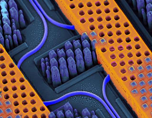 Shown in blue are the optical waveguides (and bend radius) while the copper wires carrying high-speed electrical signals are shown in orange. Source: IBM
System vendors have been on a silicon-photonics spending spree.
Cisco Systems started the ball rolling in 2012 when it acquired silicon photonics start-up, LightWire, for $272M. Mellanox Technologies more recently bought Kotura for $82M. Now Huawei has acquired Caliopa, a four-year-old Belgium-based start-up, for an undisclosed fee. The Chinese system vendor has said it is looking to further bolster its European R&D, and highlighted silicon photonics in particular.
Given that it was only just over a decade ago when systems companies were shedding their optical component units, the trend to acquire silicon photonics highlights the growing importance of the fledgling technology.
These system vendors view silicon photonics as a strategic technology. The equipment makers want to develop expertise and experience as they plan to incorporate the technology in upcoming, hopefully differentiated platforms.
"If I have a Terabit of capacity on the front panel, how am I going to manipulate that across the line card, a fabric or the backplane?" says Adam Carter, general manager and senior director of the transceiver modules group at Cisco Systems. "We saw silicon photonics as a technology that could potentially enable us to get there."
System vendors are already using embedded optics - mounted on boards close to the ICs instead of pluggable modules on the front panel - to create platforms with denser interfaces.
"Photonics doesn't need the latest and greatest lithography"
Arista Networks' 7500E switch has a line card with board-mounted optics rather than pluggable transceivers to increase 100 Gigabit port density. The company offers several line cards using pluggable modules but it has designed one card with board-mounted optics that offers flexible interfaces - 10 Gig, 40 Gig and 100 Gig - and a higher port density. When developing the design, the multi-source agreement (MSA) CFP2 pluggable module was not ready, says Arista.
Compass-EOS, a core IP router start-up, has developed chip-mounted optics based on 168 lasers and 168 detectors. The novel Terabit-plus optical interface removes the need for a switch fabric and the mid-plane to interconnect the router card within the platform. The interface also enables linking of platforms to scale the IP core router.
Both companies are using VCSELs, an established laser technology that silicon photonics competes with. Yet the two designs highlight how moving optics closer to chips enables system innovation, a development that plays to silicon photonics' strength.
 "I characterise silicon photonics as a technology that will compete in the right applications but won’t displace indium phosphide" Ed Murphy, JDSU
Silicon photonics promises cost savings by enabling vendors to piggyback on the huge investments made by the semiconductor industry. Vendors making their own products, such as optical transceivers, also promises to shake up the existing optical component supply chain.
Cisco Systems' first silicon photonics product is the proprietary 100 Gigabit optical CPAK transceiver that is undergoing qualification. By making its own optical module, Cisco avoids paying the optical module makers' margins. Cisco claims the CPAK's smaller size improves the faceplate density compared to the CFP2.
Pros and cons
Silicon photonics may be able to exploit the huge investment already made in the semiconductor industry, but it does differ from standard CMOS integrated circuits (ICs).
First, optics does not have the equivalent of Moore's Law. Whereas chip economics improve with greater integration, only a few optical functions can be cascaded due to the accumulated signal loss as light travels through the photonic circuit. This is true for optical integration in general, not just silicon photonics.
Another issue is that the size of an optical component - a laser or a modulator - is dictated by the laws of physics rather than lithography. "Photonics doesn't need the latest and greatest lithography," says Martin Zirngibl, domain leader for enabling physical technologies at Alcatel-Lucent's Bell Labs. "You can live with 100nm, 120nm [CMOS] components whereas for electronics you want to have 45nm."
This can lead to the interesting situation when integrating electronics with photonics. "You either don't use the latest technology for electronics or you waste a lot of real estate with very expensive lithography for photonics," says Zirngibl.
Another disadvantage of silicon is that the material does not lase. As a result, either a III-V material needs to be bonded to the silicon wafer or an external laser must be coupled to the silicon photonics circuit.
Silicon also has relatively small waveguides which make it tricky to couple light in and out of a chip.
The advantages of silicon photonics, however, are significant.
The technology benefits from advanced 8- and 12-inch wafers and mature manufacturing processes developed by the semiconductor industry. Using such CMOS processes promises high yields, manufacturing scale, and automation and testing associated with large scale IC manufacturing.
"This is probably the only advantage but it is very significant," says Valery Tolstikhin, founder and former CTO of indium phosphide specialist, OneChip Photonics, and now an independent consultant. "It takes silicon totally off the scale compared to any other photonics materials."
"We can build the single-die optical engine in the same CMOS line where processors are built, where billions [of dollars] of investment has been done"
IBM's high-density silicon photonics optical engine is made using a 90nm CMOS process. "We can build the single-die optical engine in the same CMOS line where processors are built, where billions [of dollars] of investment has been done," says Yurii Vlasov, manager of the silicon nanophotonics department at IBM Research. "We are riding on top of that investment."
Extra processing may be introduced for the photonics, says IBM, but the point is that there is no additional capital investment. "It is the same tooling, the same process conditions; we are changing the way this tooling is used," says Vlasov. "We are changing the process a little bit; the capital investment is in place."
 "We believe that even for shorter distance, silicon photonics does compete in terms of cost with VCSELs." Yurii Vlasov, IBM
Stephen Krasulick, CEO of silicon photonics start-up, Skorpios Technologies, makes a similar point. "The real magic with our approach is the ability to integrate it with standard, commercial fabs," he says.
Skorpios is a proponent of heterogeneous integration, or what the company refers to as 'silicon photonics 2.0'. Here silicon and III-V are wafer-bonded and the optical components are created by etching the two materials. This avoids the need to couple external lasers and to use active alignment.
"We do it in a manner such that the CMOS foundry is comfortable letting the wafer back into the CMOS line," says Krasulick, who adds that Skorpios has been working with CMOS partners from the start to ensure that its approach suits their manufacturing flow.
Applications
The first applications adopting silicon photonics span datacom and telecom: from short-reach interconnect in the data centre to 100 Gigabit-per-second (Gbps) long-distance coherent transmission.
Intel is developing silicon photonics technology to help spur sales of its microprocessors. The chip giant is a member of Facebook's Open Compute Project based on a disaggregated system design that separates storage, computing and networking. "When I upgrade the microprocessors on the motherboard, I don't have to throw away the NICs [network interface controllers] and disc drives," says Victor Krutul, director business development and marketing for silicon photonics at Intel. The disaggregation can be within a rack or span rows of equipment.
"Optical modules do not require state-of-the-art lithography or large scale photonic integration, but they do need to be coupled in and out of fibre and they need lasers - none of that silicon photonics has a good solution for"
Intel has developed the Rack Scale Architecture (RSA) which implements a disaggregated design. One RSA implementation for Facebook uses three 100Gbps silicon photonics modules per tray. Each module comprises four transmit and four receive fibres, each at 25Gbps. Each tray uses a Corning-developed MXC connector and its ClearCurve fibre that support data rates up to 1.6Tbps. “Different versions of RSA will have more or less modules depending on requirements," says Krutul.
Luxtera, whose silicon photonics technology has been used for active optical cables, and Mellanox's Kotura, are each developing 100Gbps silicon photonics-based QSFPs to increase data centre reach and equipment face plate density.
One data centre requirement is the need for longer reach links. VCSEL technology is an established solution but at 100Gbps its reach is limited to 100m only. Intel's 100Gbps module, operating at 1310nm and combined with Corning's MXC connector and ClearCurve multi-mode fibre, enables up to 300m links. But for greater distances - 500m to 2,000m - a second technology is required. Data centre managers would like one technology that spans the data centre yet is cost competitive with VCSELs.
"Silicon photonics lends itself to that," says Cisco's Carter. "If we drive the cost lower, can we start looking at replacing or future proofing your network by going to single mode fibre?"
 "There are places where silicon photonics will definitely win, such as chip-to-chip optical interconnects, and there are places where there is still a question mark, like fibre-optics interconnects." Valery Tolstikhin
IBM's 25Gbps-per-channel optical engine has been designed for use within data centre equipment. "We are claiming we have density based on optical scaling which is the highest in the industry, and we have done it using monolithic integration: optical devices are built side-by-side with CMOS," says Vlasov.
What is important, says Vlasov, is not so much the size of the silicon waveguide but how sharp its bend radius is. The bend radius dictates how sharply the light can be guided while remaining confined within the integrated circuit. The higher the light confinement, the smaller the bend radius and hence the overall circuit area.
Much progress has been made in improving light confinement over the past two decades, resulting in the bend ratio coming down from 1cm to a micron. IBM claims that with its technology, it can build systems comprising hundreds of devices occupying a millimeter. "That is a major difference in the density of optical integration," says Vlasov.
IBM does not use heterogeneous integration but couples lasers externally."It is not complicated, it is a technical problem we are solving; we believe that is the way to go," says Vlasov. "The reason why we have gone down this path is very simple: we believe in monolithic integration where electrical circuitry sits side by side with optical components."
Such monolithic integration of the optics with the electronics, such as modulator drivers and clock recovery circuitry, reduces significantly the cost of packaging and testing. "We believe that even for shorter distances, silicon photonics does compete in terms of cost with VCSELs if all elements of the cost are taken care of: bill of materials, packaging and testing," says Vlasov.
But not everyone believes silicon photonics will replace VCSELs.
For example, Tolstikhin questions the merits of silicon photonics for transceiver designs, such as for 100 Gig modules in the data centre. "There are places where silicon photonics will definitely win, such as chip-to-chip optical interconnects, and there are places where there is still a question mark, like fibre-optics interconnects," he says.
Tolstikhin argues that silicon photonics offers little advantage for such applications: "Optical modules do not require state-of-the-art lithography or large scale photonic integration, but they do need to be coupled in and out of fibre and they need lasers - none of that silicon photonics has a good solution for."
Cisco says it was first attracted to LightWire's technology because of its suitability for optical transceivers. Six years ago 1W, SFP+ modules were limited to 10km. "Customers wanted 40km, 80km, even WDM," says Carter. "They [LightWire] did a 40km SFP+ using their modulator that consumed only 0.5W - a huge differentiator." Two years ago 100 Gig CFP modules were at 24W while LightWire demonstrated a module under 8W, says Carter.
Tolstikhin believes silicon photonics' great promise is for applications still to emerge. One example is chip-to-chip communication that has modest optical light requirements and does not have to be coupled in and out of fibre.
"Here you have very high requirements for density packaging and the tiny [silicon] waveguides are handy whereas indium phosphide is too big and too expensive here," says Tolstikhin. Longer term still, silicon photonics will be used for on-chip communication but that will likely be based on deep sub-wavelength scale optics such as surface plasmonics rather than classical dielectric waveguides.
Tolstikhin also argues that the economics of using indium phosphide compared to silicon photonics need not be all that gloomy.
Indium phosphide is associated with custom small-scale fabs and small volume markets. But indium phosphide can benefit from the economics of larger industries just as silicon photonics promises to do with the semiconductor industry.
Indium phosphide is used in higher volume for wireless ICs such as power amplifiers. "Quite significantly orders of magnitude higher," says Tolstikhin. The issue is that, conventionally, photonic circuits are fabricated by using multiple epitaxial growth steps, whereas the wireless ICs are made in a single-growth process, hence epitaxy and wafer processing are decoupled.
"If you can give up on regrowth and still preserve the desired photonic functionality, then you can go to commercial RF IC fabs," he says. "This is a huge change in the economic model." It is an approach that enables a fabless model for indium phosphide photonics, with the potential advantages not unlike those claimed by silicon photonics with respect to commercial CMOS fabs.
"That suggests indium phosphide - which has all kinds of physical advantages for those applications that require transmitters, receivers and fibre, plus readily available high-speed analogue electronics for trans-impedance amplifiers and laser or modulator drivers - may be quite a competitive contender," says Tolstikhin.
"Silicon photonics has a certain capability but the hype around it has magnified that capability beyond reality"
Customers don't care which technology is used inside a transceiver. "They care only about cost, power and package density," says Tolstikhin. "Indium phosphide can be competitive and on many occasions beat silicon photonics."
JDSU also believes that long-term, a perfect fit for silicon photonics may be relative short reach interconnects – chip-to-chip and board-to-board reaches. “You need to have very high speed and dense interconnects, I can see that as being a very strong value proposition long term," says Ed Murphy, senior director, communications and commercial optical products at JDSU.
Finisar and JDSU are open to the potential benefits of silicon photonics but remain strong proponents of traditional optical materials such as indium phosphide and gallium arsenide.
"We have designed silicon photonic chips here at Finisar and have evaluations that are ongoing. There are many companies that now offer silicon photonics foundry services. You can lay out a chip and they will build it for you," says Jerry Rawls, executive director of Finisar. "The problem is we haven't found a place where it can be as efficient or offer the performance as using traditional lasers and free-space optics."
"Silicon photonics has a certain capability but the hype around it has magnified that capability beyond reality,” says JDSU's Murphy. "Practitioners of silicon photonics would tell you that as well."
According to Murphy, each application, when looked at in detail, has its advantages and disadvantages when using either silicon photonics or indium phosphide. “Even in those applications where one or the other is better, the level of improvement is measured in a few tens of percent, not factors of ten,” he says. "I characterise silicon photonics as a technology that will compete in the right applications but won’t displace indium phosphide."
Silicon photonics for telecom
At the other extreme of the optical performance spectrum, silicon photonics is being developed for long-distance optical transmission. The technology promises to help shrink coherent designs to fit within the CFP2 module, albeit at the expense of reach. A CFP2 coherent module has extremely challenging cost, size and power requirements.
Teraxion is developing a coherent receiver for CFP2. "We believe silicon photonics is the material of choice to fulfill CFP2 requirements while allowing even smaller size reduction for future modules such as the CFP4," said Martin Guy, Teraxion's vice president of product management and technology.
u2t Photonics and Finisar recently licensed indium phosphide modulator technology to help shrink coherent designs into smaller form factor pluggables. So what benefit does silicon photonics offer here?
"In terms of size there will not be much difference between indium phosphide and silicon photonics technology," says Guy. "However, being on each side on the fence, we know that process repeatability and therefore yield is better with silicon photonics." Silicon photonics thus promises a lower chip cost.
"We have projects spanning everything from access all the way to long haul, and covering some datacom as well," says Rob Stone, vice president of marketing and program management at Skorpios. The start-up has developed a CMOS-based tunable laser with a narrow line width that is suitable for coherent applications.
"If you develop a library of macrocells, you can apply them to do different applications in a straightforward manner, provided all the individual macrocells are validated," says Stone. This is different to the traditional design approach.
Adding a local oscillator to a coherent receiver requires a redesign and a new gold box. "What we've got, we can plug things together, lay it out differently and put it on a mask," says Stone. "This enables us to do a lot of tailoring of designs really quite quickly - and a quick time-to-market is important."
Perhaps the real change silicon photonics brings is a disruption of the supply chain, says Zirngibl.
An optical component maker typically sells its device to a packaging company that puts it in a transmitter or receiver optical sub-assembly (TOSA/ ROSA). In turn, the sub-assemblies are sold to a module company which then sells the optical transceiver to an equipment vendor. Each player in the supply chain adds its own profit.
Silicon photonics promises to break the model. A system company can design its own chip using design tools and libraries and go to a silicon foundry. It could then go to a packaging company to make the module or package the device directly on a card, bypassing the module maker altogether.
Yet the ASIC model can also benefit module makers.
IBM has developed its 25Gbps-per-channel silicon photonics technology for its platforms, for chip-to-chip and backplanes, less for data centre interconnect. But it is open to selling the engine to interested optical module players. "If this technology can be extended to 2km for big data centres, others can come in, the usual providers of transceivers," says Vlasov.
"There are companies with the potential to offer a [silicon photonics] design service or foundry service to others that would like to access this technology," says Cisco's Carter. "Five years ago there wasn't such an ecosystem but it is developing very fast."
The article is an extended version of one that appeared in the exhibition magazine published at ECOC 2013.
Part 1: Optical interconnect, click here
Part 2: Bell Labs on silicon photonics, click here
Q&A with Jerry Rawls - Part 2
The concluding part of the interview with Finisar's executive chairman and company co-founder, Jerry Rawls, to mark the company's 25th anniversary.
Second and final part

Guys that are in the silicon photonics industry have a religion. It does not make any difference what the real economics are, what the real performance is, they talk with a religious fervour about what might be possible with silicon
Q: Over 25 years, what has been one of your better decisions?
Jerry Rawls: After the crash of 2001, we asked what are we going to do in the optics business? Are we going to stay in it? Is there a bright future? And if so, how are we going to respond to it?
We still believed that this was an attractive market and we had built an important brand. And, we knew we could make it more successful in the future, but we were going to have to change the way we did business.
Deciding to become vertically integrated was the key change. At that time, every other company was trying to sell their assets and remove their fixed costs. They were outsourcing manufacturing instead of bringing it in-house. Everyone wanted a variable cost business model, not a fixed cost model. We clearly went against the mainstream.
That is one of the better decisions we ever made.
Equally, with the benefit of hindsight, what do you regret?
A couple of acquisitions that we made in our early years turned out less than desirable. We were sold some technology for which we believed the probability of success was high. We bought the companies based on their technology, not necessarily on their business, and it did not pan out. One thing we learned from those experiences is that when we buy a company, we try to be much more careful about our due diligence.
Another one I regret, although I don't think it was a bad decision: We had created a division in the company called Network Tools that was the leading company in the SAN (storage area network) industry for protocol analysis.
Every company in the world that was creating SAN equipment bought our protocol analysers for Fibre Channel. That was about a $40 million-a-year business and nicely profitable. We sold it [to JDSU] in 2009 and I regret that because we started that business from scratch. It really helped create the SAN industry; it helped our customers prove their equipment interoperability.
We sold it because we had that $250 million in debt we had to pay off. We had borrowed the money and it was now due. It [2009] was still not a great time, we were trying to raise cash and one asset that had value was this division.

How would you describe the current state of the optical component industry and the main challenges it faces?
The optical component industry is in a pretty healthy place. For the most part, the larger companies are doing quite well. Our business is doing nicely. We have had four quarters in a row where revenues have grown, our profitability metrics are improving and our outlook is good. A lot of that has to do with our focus on the data centre market.
We anticipate increasing dollars spent worldwide by phone companies over the next five years
The speeds and feeds in data centres are increasing dramatically: data centres are becoming larger, the connections are faster - connections that used to be copper back in the days of Gigabit Ethernet are now at 10 Gigabits and mostly optical. That transformation of copper to optics that took place in the telephone world 35 years ago is now in full bloom in the data centres. So it is a great time to be in optics because the trends are rolling our way.
We are anticipating spending growth in the telecommunications world with an upgrade in global networks to deal with growing Internet traffic. These networks are changing to very sophisticated ROADM [reconfigurable optical add/drop multiplexer] architectures and 100 Gigabit transmission rates.
We anticipate increasing dollars spent worldwide by phone companies over the next five years. So that sector is going to become healthier and hopefully a larger percentage of our business.
I believe the optical component industry has a number of market opportunities that are going to keep it pretty healthy for some time.
It does not mean that we don't have challenges. The industry, and in particular telecommunications, is fragmented. There are a number of competitors that have very small market share. Many of these competitors are focussing their R&D efforts on the same products - the next generation of telecom equipment - and that is very inefficient. That is the main challenge that the optical industry has, that this fragmentation leads to inefficiency.
That limits the margins of the companies and the industry. It also means that pricing in the industry is at a lower level than component suppliers would like to see.
How that works out is not clear. You could say that in a fragmented industry, you would like to see more consolidation. There will be a little of that. But there are some parts of the industry where consolidation will be very slow.
For example, all of the Japanese optical suppliers are likely to stay in business for some time. Almost every big Japanese electronics company has an optical division, and they always have. None went out of business in the crash of '01 and none went out in the crash of '08 – ’09. That is because these optics divisions are small parts of giant conglomerates. This fragmentation problem is difficult to solve.
Datacom and the data centre appear to be a more interesting segment in terms of driving change than telecom. How do you view the two segments going forward?
I think both are interesting.
The data centre is interesting because of the increased density of Gigabits-per-square-inch on the faceplates of equipment, whether it is switches, storage or servers. Then there is the faster connection speeds between devices and the demand for low latency. The physical size of some of these data centres is demanding that certain connections become single mode - more like wiring a campus as opposed to multi-mode historically used in single buildings.
The datacom market is also very interesting because of a number of connections changing from copper to optical as speeds get faster. Copper transmission demands too much power through big cables at these higher speeds.
In telecom, today what is really exciting is the advent of coherent transmission systems, in particular at 100 Gigabits moving to 400 Gigabit and 1 Terabit-per-second in the next decade.
Coherent transmission is revolutionary in that by using electronics rather than optics to do signal correction for long distance fibre transmission, these signals can be much more efficient, run faster and be much less costly than they have ever been in the past.
Coupled with that is the automation of these optical networks through the extensive use of sophisticated ROADMs. With the next generation of networks, truck rolls to do provisioning and reconfigurations will be almost eliminated.
So there is a lot of excitement for us just because of what is coming to telecom networks. We have been through a lull for the last couple of years but it is a cyclical industry that tends to follow technology waves. We are entering the 100 Gigabit transmission wave and the sophisticated use of many, many ROADMs in these networks for automation.
We have designed silicon photonic chips here at Finisar and have evaluations that are ongoing
Silicon photonics is spoken of as a disruptive technology for datacom and telecom. It also promises to disrupt the component supply chain. What is Finisar's take on the technology?
As a company, we are very product focussed and we want to deliver transmission products and switching products, etc. that fulfill our customers' needs. We don't really care what the technology is. We are going to invest in technology that enables us to build the highest performing and most efficient devices that we can.
Silicon photonics is an interesting technology. We haven't used it in any of our products so far with the exception of a silicon waveguide in an integrated receiver. The most interesting thing about silicon photonics is not just to be able to make waveguides for multiplexers or demultiplexers, but to make modulators.
People have been speculating for years that we will have to use external modulators to achieve higher transmission speeds as we won’t be able to directly drive a laser fast enough.
We make VCSELs by the tens of millions. When we were making them at one Gigabit-per-second [Gbps], there were those in the industry that predicted that we would never be able to run at 2 Gbps as it would be impossible to modulate the lasers that fast. Then we did 2 Gbps, and then there were those that said it would be impossible to do 4, 8 or 10 Gigabits. Well, we are shipping devices today that are 25Gbps VCSELs that are directly modulated.
At every one of those steps there were people investing in silicon photonics companies because they could build modulators they thought would run that fast. I believe every one of those silicon photonics companies went broke.
We now have a new wave of silicon photonics companies. And because Cisco Systems happened to buy one [LightWire], there has been a lot of excitement about silicon photonics.
Well, the physics are such that it is always more efficient to directly modulate a laser - that is, to drive it with an injection of current - than it is to have a continuous wave laser where you externally modulate the light. The external modulation takes more power, more components and more cost.
Guys that are in the silicon photonics industry have a religion. It does not make any difference what the real economics are, what the real performance is, they talk with a religious fervor about what might be possible with silicon.
To date, no one has been able to make light out of silicon. That means one can make a silicon modulator and a silicon waveguide but still have to buy an indium phosphide laser to create light. Then they would have to bond that laser to the silicon substrate in a way that it efficiently launches light, is mechanically stable, and hermetic and that it will stand the rigours of all these networks. That means it can be deployed for 10 or 20 years over temperatures of 0 to 85 degrees C, and survive the qualification torture tests of high humidity, high heat and temperature cycling.
One of the things in the silicon photonics industry to date has been that the packaging - and therefore the yields - have been so difficult, such that the costs have been very high.
I promise you today that for almost every application, silicon photonics costs are higher than using traditional indium phosphide and gallium arsenide lasers and direct modulation.
We don't ignore silicon photonics as a potential technology.
We have designed silicon photonic chips here at Finisar and have evaluations that are ongoing. There are many companies that now offer silicon photonics foundry services. You can lay out a chip and they will build it for you.
We can go to a foundry; we can use their design rules and libraries and design silicon modulators and waveguides and put together a chip with as many splits and Mach-Zehnders that we want. The problem is we haven't found a place where it can be as efficient or offer the performance as using traditional lasers and free-space optics.
Our packaging has been more efficient and our output has been at a higher performance level. Remember that silicon is optically quite lossy. That means you have to launch a lot of light into it to get a little light out.
So far we just haven't found a product where we thought silicon photonics modulation was as efficient as we could build using some other technology. That is true today.
We may use silicon photonics one of these days. In fact, if we look back five or 10 years ago, when we predicted what we would need to build a 100 Gig transponder, silicon photonics was one of our alternatives, and one of the paths we went down in parallel in completing the design.
As it turns out, traditional optics and micro-optical components exceeded our own expectations.
I compare it to the disc drive industry. Twenty years ago people were predicting the demise of the disc drive industry because of solid state memory. It was thought impossible that disc drives would be around five years hence. Well, the guys in the disc industry learned how to increase the bit density and the resolution of the heads and look at the industry today. You can buy a Terabyte drive for less than a hundred dollars. The amazing technology advances they have made have kept them in the game.
What are the biggest challenges facing Finisar?
The biggest challenge we face is meeting the changes in the industry. The use of information is becoming so pervasive - video everywhere and 4G networks - that means all the kids are going to be streaming HD video to some device in their hand. And there is going to be billions of them.
Also, another challenge is managing the expectations of our customers - the equipment companies - in terms of delivering the speeds, densities and the low power performance needed to provide all this information.
It is a daunting task.
We have customers today trying to design systems that will have Terabit-per-second optical links. We don't know how we are going to get there yet but I promise you we will.
The industry in 25 years' time: Still datacom & telecom or something else by then?
In 25 years' time, datacom and telecom will be much more converged.
The data center today is becoming more like wiring a campus network than it is wiring a building as the distances become larger and the speeds faster. Today in data centers we only use point-to-point connections; we use no multiple wavelengths on fibres.
In the telephone world, everything is WDM. Today we are using mostly 96 wavelengths on a single fibre. Those 96 channels can all run at 100 Gbps – a total of nearly 10 Terabit on a single fiber. In the data center world most connections are single wavelengths, point-to-point. But in 25 years, the data centers are going to be using many of the techniques that are used in the telecom networks today in terms of making efficient use of fibres, using multiple colors of light, and being able to switch those individual colours.
For the first part, click here
Terabit interconnect to take hold in the data centre
Intel and Corning have further detailed their 1.6 Terabit interface technology for the data centre.
The collaboration combines Intel's silicon photonics technology operating at 25 Gigabit-per-fibre with Corning's ClearCurve LX multimode fibre and latest MXC connector.
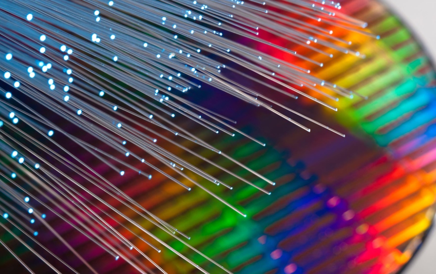 Silicon photonics wafer and the ClearCurve fibres. Source: Intel
The fibre has a 300m reach, triple the reach of existing multi-mode fibre at such speeds, and uses a 1310nm wavelength. Used with the MXC connector that supports 64 fibres, the overall capacity will be 1.6 Terabits-per-second (Tbps).
"Each channel has a send and a receive fibre which are full duplex," says Victor Krutul, director business development and marketing for silicon photonics at Intel. "You can send 0.8Tbps on one direction and 0.8Tbps in the other direction at the same time."
The link supports connections within a rack and between racks; for example, connecting a data centre's top-of-rack Ethernet switch with an end-of-row one.
James Kisner, an analyst at global investment banking firm, Jefferies, views Intel’s efforts as providing important validation for the fledgling silicon photonics market.
However, in a research note, he points out that it is unclear whether large data centre equipment buyers will be eager to adopt the multi-mode fibre solution as it is more expensive than single mode. Equally, large data centres have increasingly longer span requirements - 500m to 2km - further promoting the long term use of single mode fibre.
Rack Scale Architecture
The latest details of the silicon photonics/ ClearCurve cabling were given as part of an Intel update on several data centre technologies including its Atom C2000 processor family for microservers, the FM5224 72-port Ethernet switch chip, and Intel's Rack Scale Architecture (RSA) that uses the new cabling and connector.
Intel is a member of Facebook's Open Compute Project based on a disaggregated system design that separates storage, computing and networking. "When I upgrade the microprocessors on the motherboard, I don't have to throw away the NICs [network interface controllers] and disc drives," says Krutul. The disaggregation can be within a rack or between rows of equipment. Intel's RSA is a disaggregated design example.
The chip company discussed an RSA design for Facebook. The rack has three 100Gbps silicon photonics modules per tray. Each module has four transmit and four receive fibres, or 24 fibres per tray and per cable. “Different versions of RSA will have more or less modules depending on requirements," says Krutul. Intel has also demonstrated a 32-fibre MXC prototype connector.
Corning says the ClearCurve fibre delivers several benefits. The fibre has a smaller bend radius of 7.5mm, enabling fibre routing on a line card. The 50 micron multimode fibre face is also expanded to 180 microns using a beam expander lens. The lenses make connector alignment easier and less sensitive to dust. Corning says the MXC connector comprises seven parts, fewer than other optical connectors.
Fibre and connector standardisation are key to ensure broad use, says Daryl Inniss, vice president and practice leader, components at Ovum.
"Intel is the only 1310nm multimode transmitter and receiver supplier, and expanding this optical link into other applications like enterprise data centres may require a broader supply base," says Inniss in a comment piece. But the fact that Corning is participating in the development signals a big market in the making, he says.
Intel has not said when the silicon photonics transceiver and fibre/ connector will be generally available. "We are not discussing schedules or pricing at this time," says Krutul.
Silicon photonics: Intel's first lab venture
The chip company has been developing silicon photonics technology for a decade.
"As our microprocessors get faster, you need bigger and faster pipes in and around the servers," says Krutul. "That is a our whole goal - feeding our microprocessors."
Intel is setting up what it calls 'lab ventures', with silicon photonics chosen to be the first.
"You have a research organisation that does not do productisation, and business units that just do products," says Krutul. "You need something in between so that technology can move from pure research to product; a lab venture is an organisational structure to allow that movement to happen."
The lab ventures will be discussed more in the coming year.
Coriant adds optical control to SDN framework
Coriant's CTO, Uwe Fischer, explains its Intelligent Optical Control and how the system will complement Transport SDN.
"You either master all that complexity at once, or you find the right entry point and provide value for each concrete challenge, and extend step-by-step from there"
Uwe Fischer, CTO of Coriant
Coriant has deployed a networking framework that it says will comply with Transport SDN, the software-defined networking (SDN) implementation for the wide area network (WAN).
The company's Intelligent Optical Control system is already deployed with one large North American operator while Coriant is working to install the system with other Tier 1 customers.
Work to extend SDN technology beyond the data centre to work across operators' transport networks has just begun. The Open Networking Foundation (ONF), for example, has established an Optical Transport Working Group to define the extensions needed to enable SDN control of the transport layer and not just packet.
"SDN and optical networking go together nicely; they are not decoupled but make up an end-to-end overall framework," says Uwe Fischer, CTO at Coriant.
The Intelligent Optical Control is designed to tackle immediate networking issues as Transport SDN is developed. Coriant says its system complies with the ONF's three networking layer SDN model. The top, application layer interfaces with the middle, control layer. And it is at the control layer where the SDN controller oversees the network elements found in the third, infrastructure layer.
Intelligent Optical Control adds two other components to the model. An extra intelligence component in the control layer that sits between the SDN controller and the infrastructure layer. This intelligence is designed to exploit the intricacies of the optical layer.
Coriant has also added an application at the topmost layer to automate operational procedures. "SDN at the application layer is centered around service creation," says Fischer. "We see a complete set of other applications which automate operational workflows."

Optical intelligence
One key benefit of SDN is the central view it has of the network and its resources. Such centralised control works well in the data centre and packet networking. Operators' networks are more complex, however, housing multiple vendors' equipment and multiple networking layers and protocols.
The ONF's Optical Transport Working Group is investigating two approaches - direct and abstract models - to enable the OpenFlow standard to extend its control across all the transport layers.
With the direct model, an SDN controller will talk to each network element, controlling its forwarding behaviour and port characteristics. The abstract model, in contrast, will enable the controller to talk to a network element or an intermediate controller or 'mediation'. This mediation performs a translator role, enacting requests from the SDN controller.
The direct model interests certain ONF members due to its potential of reduce the cost of networking equipment by moving much of the software from each element to the SDN controller. The abstract model, in contrast, has the benefit of limiting how much the controller needs to be exposed to the underlying network's details.
Coriant says it has yet to form a view as to the benefits of the direct and abstract ONF models. That said, Fischer does not see any mechanisms being discussed in the ONF that will fully exploit the potential of the photonic network. Accordingly, Coriant has added its own intelligence that sits between the SDN controller and the photonic layer.
“We fully comply with the approach of an SDN controller, however, we put another layer in between the control layer and the infrastructure layer,” says Fischer. “We consider it a part of the control layer, but adding the planning and routing intelligence to leverage the full performance of the infrastructure layer underneath."
Fischer says there is a role for abstraction at the photonic layer but perhaps only for metro networks. "We currently don't think this will really extend to the wide area photonic layer," he says.
"The added intelligence can leverage the full performance of the WDM network because it knows all the planning rules in detail," says Fischer. It does multi-layer optimisation across the transport layers. Coriant has added the intelligence because it does not think the transport-network-specific aspects can be centralised in a generic way.
Automated operations
Coriant's Intelligent Optical Controller also adds an application to automate operational procedures. Fischer cites how the application layer component benefits the workflow when a service is activated in the network.
With each service request, the Intelligent Optical Control details whether the new service can be squeezed onto existing infrastructure and details the service performance parameters to be expected, such as latency and the guaranteed bandwidth. "The operator can immediately judge the service level they would get," says Fischer.
Another planning mode supports the adding of equipment at the infrastructure layer. This enables a comparison to be made as to how the service level would improve with extra equipment in place.
If the operator can justify that business case for new hardware, the workflow is then automated. The tool creates the bill of materials, the electronic order, and the configuration and planning data needed to implement the hardware in the network.
Coriant says equipment and services can be time-tagged. If an engineer is known to be visiting a site once the hardware becomes available, the card can be pre-assigned and automatically used once it is plugged in. "There is a full consistency as to how the hardware is managed and optimised towards service creation," says Fischer.
Coriant is working with its major customers to create a testbed to demonstrate an SDN implementation of IP-over-DWDM. "It will involve interworking with third-party routers, and using SDN controllers to control the packet part of the network with Openflow and other mechanisms, and then connected to the Intelligent Optical Controller."
The goal is to demonstrate that Coriant's approach complies with this use case while better exploiting the optical network's capabilities.
Fischer says optical networking is moving to a new phase as transmission speeds move beyond 100 Gigabit.
"We are entering an interesting phase as capacity and reach hit the limits of practical networks," he says. "This means we are talking about flexible modulation formats and variously composed super-channels for 400 Gigabit and 1 Terabit."
In effect, a virtualisation of bandwidth is taking place at the photonic layer. "This fits nicely into the SDN principle as on the one hand it virtualises capacity, which very much fits in the model of virtualising infrastructure."
But it also brings challenges.
"There is currently not a good practical means to manage such flexible capacity at the photonic layer," says Fischer. This, says Coriant, it what its customers are saying. It also explains Coriant's decision to add the optical controller. "You either master all that complexity at once, or you find the right entry point and provide value for each concrete challenge, and extend step-by-step from there," says Fischer.
Interview with Finisar's Jerry Rawls
Finisar is celebrating its 25th anniversary. Gazettabyte interviewed Finisar's executive chairman and company co-founder, Jerry Rawls, to mark the anniversary.
Part 1
 Jerry Rawls, Finisar's executive chairman and co-founder
Q: How did you meet fellow Finisar co-founder Frank Levinson?
JR: I was a general manager of a division at Rachem, a company in Menlo Park, California. We were developing and manufacturing electric interconnect products; our markets were mostly defence electronics and the computer industry.
Our customers were starting to talk a lot about fibre optics and we had no products. It seemed like it was going to be a hole in our portfolio. So I started a fibre optics product development group and hired a bright young physicist from Bell Labs to be the principal technologist. His name was Frank Levinson.
What decided you both to set up Finisar?
The division I was running was very successful: we were the fastest growing and the most profitable. Frank was lured away by our chairman to work on a fibre-optics start-up that was internally funded: Raynet.
Raynet lost almost a billion dollars over the next few years. It was the biggest venture loss in the history of Silicon Valley, and it may still be the biggest venture capital loss in Silicon Valley history.
At they were losing money, and it was sucking money from the rest of the company, our division was unable to fund a lot of projects we would have liked to have funded if we were to continue to grow. Frank was very frustrated as they were jousting at windmills.
We had lunch one day and talked about the possibility of starting a fibre-optics company. It was as simple as that: we could do better on our own. This was in 1987.
What convinced you both that high-speed fibre optics was a business to pursue?
 Frank LevinsonFrank had some original patents from Bell Labs on wavelength division multiplexing (WDM) and the use of fibre optics in telephony. That is where fibre optics first had a major impact.
As we started a little company, the thing that was happening in 1988 was that the Mac OS had just been introduced and Windows was right behind it. This was the first time colour and graphics were introduced to the PC. As we watched the change to graphics and colour, we knew video was not going to be too far behind. It was clear that files would be larger, and the bandwidth between systems, and between storage and systems, would need to be greater.
And so we started to think about high-speed optics for data centres. And the corollary to that was low-cost, high-speed optics for data centres.
We did not think we were up to competing with the telecommunications industry because in those days AT&T Bell Labs (Lucent), Alcatel and Nortel dominated the world of fibre optics. They built their own components, they built their own sub-systems and we did not think there was any chance of a start-up competing with them.
But in the world of computer networks, there were no established suppliers as fibre optics was almost non-existent there. Our goal was to focus on Gigabit-per-second speeds and how we could build low-cost Gigabit optical links for data centres.
The reason low cost was so important was that to buy an OC-12 (622 Megabit-per-second SONET) link, the cost was thousands of dollars at each end. This was a telephony fibre link but there was no chance you could be successful in any sort of computer installation with an optical connection at such prices.
So the question was: How do you bring the cost down and the prices down to a level that networks could afford, and that were priced lower than the computers at each end?
"Frank and I started the company with our own money. We had no outside investors. I took a second mortgage on my house and off we went to start a company"
So we looked for compromises. One was distance. OC-12s went 20km, 40km, 80km but data centres only needed a few hundred meters. Ok, if we can build a link that goes 500m, we have covered any data centre in the world.
The next thing was: What does that open up? And what can we do? It quickly led us to multi-mode transmission, and multi-mode transmission turned out for us to be much, much cheaper to build because the core of the fibre was either 50 or 62.5 microns versus 8 microns in telephony fibre. That means that the core is enormous compared to telephone fibres, and our job for alignment [with the laser] was that much easier.
We built some early samples. We went through several iterations to get there. We put together the components and ICs and we finally had a product that we thought was pretty good. We had a 1 Gigabit transmitter with 17 pins and a 1 Gigabit receiver with 17 pins, and we had a Gigabit transceiver with 28 pins.
Our first customers for these devices were the national laboratories. Lawrence Livermore National Lab was one of the pioneers in the world of Fibre Channel. They, working with IBM, had a big hand in the whole Fibre Channel protocol.
Our engagement with Lawrence Livermore led to other labs. All these physicists, building high-energy physics experiments, all of a sudden started buying these optical transceivers from us by the thousands. That was our first product.
Finisar's initial focus included consulting. What sort of things was the company doing during this period?
Consulting, we did a tiny bit. Mostly, what we did was contract design engineering.
Frank and I started the company with our own money. We had no outside investors. I took a second mortgage on my house and off we went to start a company. That meant we had to be able to support ourselves and our employees. We had to have customers that pay their bills.
 Early optical transceiver product from Finisar
So one of the things we did in the early days is we found customers to do design work for. We designed fibre optic systems, we designed cable TV fibre optics systems, we designed special fibre interconnects, we did some special fibre testing - which you might call consulting. We designed a scuba-diver computer that calculated dive tables - whether you would get the bends or not, how long you could stay down, and what depth and pressure. We designed a swimming pool chlorination control system.
We did a lot of things along the way to generate revenue to support our simultaneous product development work to build the Gigabit optics devices.
We didn't start the company to be a contract design house; we started it to be a product company. But the financial reality was we had to have enough money coming in to support our employees and ourselves.
"His firm had so much inventory of the products from that company that he didn’t think they would buy anything for the next three or four years"
In the late 1990s, Finisar experienced the optical boom and then the crash. Do you recall when you first realised all was not well?
In November and December of 2000, we were about to acquire two companies. Both were component suppliers in the telecommunications industry. They both sold to big customers like Alcatel, Nortel and Lucent.
In the due-diligence process for one of the companies, I was on a phone call with Lucent who had been a huge customer – maybe 40 percent of their business came from Lucent. Talking to the VP of procurement about his history with this company and what his company’s future prospects were - all the things you do normally do in due diligence - he confirmed what his previous business had been and that he was satisfied with them as a supplier. They were a good company.
But, as we talked about future business, he went silent. And, then he came back with some devastating news: his firm had so much inventory of the products from that company that he didn’t think they would buy anything for the next three or four years. This fact was unknown to the company we were acquiring. That was my first signal that something bad was going on.
We did not acquire this company. We were in the late stages of the acquisition discussions – talking to their customers is usually one of the last things you do in due diligence – but there was obviously a material adverse change in the outlook of this company. So, we quickly terminated discussions.
A very similar thing happened with the other company only a couple of weeks later. This was late 2000, it was clear the bell was ringing. Something bad was about to happen in the optics, telephony, networking industry.
In our January quarter of 2001, we could see the incoming order rate falling. And by our February-April quarter that year, our revenues had dropped something like 47 percent in two quarters. It rolled through the industry pretty fast.
How did Finisar navigate the turbulent aftermath?
We were in a bit in shock, as most of the industry was.
To put it in perspective, our revenues dropped 47 percent in two quarters; Nortel’s High Performance Optical Components division, which had sales in one quarter during 2000 of $1.4 billion, their revenues dropped to something like $28 million. Some 98.5 percent of their revenue disappeared, it was that disastrous a time, particularly in telecom.
The issue with Finisar was that the business we built was predominantly about computer networks. We didn’t have that much business with telecom. We were selling optics for data centres and so our business didn’t decline as much as the Nortels, Alcatels and the Lucents. But it was still a precipitous decline and so we had to decide: Were we still going to stay in this business or were we going to open a hamburger stand or some other kind of a business? And our answer was we didn’t know much about the hamburger business or any other business.
We thought that, long term, fibre optics was going to be a good business. The use of information was only going to increase and that was a place where we had built a fundamental market position and we ought to continue.
To do that, we had to change our spots, that is, change our way of doing business. We were going to have to be more cost competitive. Enormous capacity had been created in the optics industry in the '90s and that capacity didn’t all evaporate [with the bust]. We knew we were going to have to be much more cost-competitive.
We decided that our strategy was to be a vertically-integrated company. In the ‘90s we were not vertically integrated: we bought lasers from the Japanese or Honeywell who made VCSELs, we bought photo-detectors from either US or Japanese suppliers, we bought ICs from merchant semiconductor companies, and we put it all together. We even outsourced all of our assembly and manufacturing. But in the future, we were convinced that we had to be more cost-competitive.
"One of the things that I think is really important here is that we allow people to make mistakes"
During this period Finisar had an IPO. How did it impact the company and this strategy?
We had previously had an IPO in 1999 that raised some money. The first thing we did after the crash was to buy a factory in Malaysia. This was around March 2001, business had started to crash, everyone was selling, and if you were buying, you could get a pretty good deal on almost anything. So we bought this factory from Seagate – 640,000 sq. ft. of almost brand new building, with 200,000 sq. ft. of clean room, 20 acres of land – we bought it for $10 million.
Then we decided we had to be vertically integrated with our ICs. We weren’t going to start an IC foundry but we had to start an IC design group. So we hired a senior IC design manager from National Semiconductor who had led their analogue design efforts and we started a semiconductor design group. Today we design almost all of the ICs that go into our datacom products. We have some 60 people worldwide who are involved in IC design, layout, testing and verification.
Next, we bought the Honeywell VCSEL fab. They were our big supplier, we were their largest customer. Honeywell decided that that business was not strategic and so we bought it.
We also bought a small laser fab in Fremont, California to make edge-emitting lasers. We could also make photo-detectors in both those fabs. So we were now in a position we could make photo-detectors and lasers, and we could design ICs and go to foundry with them instead of buying them from merchant semiconductor companies and pay their margins.
We had a beautiful big factory we could build our products in, and expand for years to come. We are still expanding in that factory. Today we have over 5,000 employees in that plant in Malaysia.
To finance all the tomfoolery, we needed a lot more money than we were able to raise with our IPO. I went to New York and Boston and peddled a convertible bond issue for $250 million. So we raised a enough cash that we could finance these acquisitions and also support the company through this crash and downturn.
It was great we were a public company because we couldn’t raise that much money if we had been a private company. It worked out well; and we eventually paid all that debt off.
Fast-forward to today, we are targeting more than a billion dollars in revenue this year, we are the largest company in our industry and I think we are the most profitable.
In 2006 IEEE Spectrum Magazine ranked Finisar top in terms of patent power among telecom equipment manufacturers. Is this still a key strategic goal of Finisar? And if so, how do you ensure innovation continues year after year?
I wouldn’t say patents are a strategic goal of ours. The IEEE Spectrum ranking was based on the number of patents you had, how many you had issued recently, but it also was importantly weighted by how many times your patents were referenced by other patent applications. A lot of ours were referenced by others who were filing patents. We ended up pretty high on the list.
We do have over 1,000 issued US patents, and we have about 500 issued international patents. We employ maybe as many as 1,300 engineers and almost 300 of them have Ph.Ds. We will continue to innovate. We have been a leader in this industry for years. Our goal is to try to be out in front, to deliver the products that meet the speeds, the power, the density that our customers need for high-speed transmission. That means we have to have a lot of talented people, we have to be focussed. And, I promise you that innovation is very important to our success.
It is not so much about how many patents we get issued. Patents are important many times for defensive purposes as much as anything else. People can’t come after us and sue us frivolously for patent infringement because we have so many patents that cover products they likely make. In the end, patents for defence is really important.
Is there something that you have learnt over the years that has proved successful regarding innovation?
First, we want to be an innovative company. When we hire, we look for innovative people, we look for clever people, smart people, but also people with good interpersonal skills, that is a part of our culture.
But one of the things that I think is really important here is that we allow people to make mistakes. We don’t encourage people to make mistakes but we allow people to make mistakes. If they are trying to do their job and they make a mistake, we don’t fire them. We try to learn from the mistakes.
Over time, we have had guys make what appeared to be pretty serious mistakes that I am sure people might have been fired for in many other companies. But, for us, we are supportive of our employees. As long as we know they are not being lazy or dishonest, we support them.
I think that environment where you can try to innovate, you can work on projects but you know the culture of the company is not vengeful and that we will tolerate mistakes is an important part of our innovative environment.
For the second and final part, click here
OIF defines carrier requirements for SDN
The Optical Internetworking Forum (OIF) has achieved its first milestone in defining the carrier requirements for software-defined networking (SDN).

The orchestration layer will coordinate the data centre and transport network activities and give easy access to new applications
Hans-Martin Foisel, OIF
The OIF's Carrier Working Group has begun the next stage, a framework document, to identify missing functionalities required to fulfill the carriers' SDN requirements. "The framework document should define the gaps we have to bridge with new specifications," says Hans-Martin Foisel of Deutsche Telekom, and chair of the OIF working group.
There are three main reasons why operators are interested in SDN, says Foisel. SDN offers a way for carriers to optimise their networks more comprehensively than before; not just the network but also processing and storage within the data centre.
"IP-based services and networks are making intensive use of applications and functionalities residing in the data centre - they are determining our traffic matrix," says Foisel. The data centre and transport network need to be coordinated and SDN can determine how best to distribute processing, storage and networking functionality, he says.
SDN also promises to simplify operators' operational support systems (OSS) software, and separate the network's management, control and data planes to achieve new efficiencies.
SDN architecture
The OIF's focus is on Transport SDN, involving the management, control and data plane layers of the network. Also included is an orchestration layer that will sit above the data centre and transport network, overseeing the two domains. Applications then reside on top of the orchestration layer, communicating with it and the underlying infrastructure via a programmable interface.
"Aligning the thinking among different people is quite an educational exercise, and we will have to get to a new understanding"
"The orchestration layer will coordinate the data centre and transport network activities and give, northbound, easy access to new applications," says Foisel.
A key SDN concept is programmability and application awareness, he says. The orchestration layer will require specified interfaces to ease the adding of applications independent of whether they impact the data centre, transport network or both.
Foisel says the OIF work has already highlighted the breadth of vision within the industry regarding how SDN should look. "Aligning the thinking among different people is quite an educational exercise, and we will have to get to a new understanding," he says.
Having equipment prototypes is also helping in understanding SDN. "Implementations that show part of this big picture - it is doable, it is working and how it is working - is quite helpful," says Foisel.
The OIF Carrier Working Group is working closely with the Open Networking Foundation's (ONF) Optical Transport Working Group to ensure that the two group are aligned. The ONF's Optical Transport Group is developing optical extensions to the OpenFlow standard.
Bell Labs on silicon photonics
Briefing: Silicon Photonics
Part 2: A system vendor's perspective
- Silicon photonics as a technology has its challenges
- Its biggest impact could be to shake up the industry's optical component supply chain
- Silicon photonics will not displace VCSELs

An interview with Alcatel-Lucent Bell Labs' Martin Zirngibl, domain leader for enabling physical technologies, on the merits and potential impact of silicon photonics
Martin Zirngibl admits he is skeptical when it comes to silicon photonics. "There is a lot of hype around silicon photonics but there are also some real advantages," he says. "We have a strong silicon photonics programme inside Bell Labs and I tell my folks: If you prove me wrong, I'm going to be very happy."
The skepticism stems from the technology's limitations. "There is no Moore's Law in photonics, you cannot cascade many photonic elements," says Zirngibl.
Photonic components are also analogue. Once several devices are cascaded, the signal loss accumulates. This is true for photonic integration in general, not just silicon photonics.
Another issue is that the size of an optical component such as a laser or a modulator is dictated by the laws of physics rather than lithography, used to make ever-smaller transistors with each generation of CMOS process. Zirngibl compares optical transmitters and receivers to cars: they improve with time but the fundamental size does not change.
"Silicon photonics could form an ASIC-like model and break the supply chain"
A consequence of shrinking feature size with semiconductors is that chip performance gets better with integration. Integration in photonics, in contrast, involves compromise and a tradeoff in optical performance.
However, the advantages of silicon photonics are significant. The technology can benefit from the huge investment made in the semiconductor industry. "CMOS foundries exists with 8- and 12-inch wafers," says Zirngibl. These mature processes are extremely well controlled, producing high-yielding devices. "If you match any component with that type of process, you have instant high volume and instant scalability," says Zirngibl.
Silicon photonics may require something different but if it can use these CMOS processes, the result is a free ride on all this investment, he says: "That is the real advantage.”
For Zirngibl, the impact of silicon photonics will more likely be on the industry supply chain. An optical component maker may sell its device to a packaging company that puts it in a transmitter or receiver optical sub-assembly (TOSA/ROSA). In turn, the sub-assemblies are sold to a module company which then sell the optical transceiver to an equipment vendor. Each player in the supply chain adds its own profit.
Silicon photonics promises to break the model. A system company can design its own chip and go to a silicon foundry. It could then go to a packaging company to make the module or package the device directly on a card, bypassing the module maker altogether.
"Silicon photonics could form an ASIC-like model and break the supply chain," says Zirngibl. "This worries the large module makers of the world."
"The problem with coherent is that it needs a lot of optical stuff"
Zirngibl stresses that such a change could also happen with traditional optical components. A system vendor could adopt a similar strategy with indium phosphide chips, for example. But the issue is that indium phosphide does not share the mature processes or the scale of the semiconductor industry, and as such an ASIC model is harder to achieve.
"If you can use CMOS processes for optical components then, all of a sudden, optical could become an ASIC-like supply chain," says Zirngibl. "It could cut out a lot of the module and package vendors."
That is what Cisco Systems has done with its CPAK module based on silicon photonics. "Cisco broke the supply chain model by doing an internal development of a module, they don't rely on anyone else," he says.
Challenges
Silicon photonics faces several challenges. One is silicon has no optical source. “A regular CMOS process will not product a light source." Companies are pursuing several approaches as to how best to couple a III-V source to silicon.
Another issue is that the optical performance of a silicon photonics design must match that of alternative solutions. "At the end of the day in photonics it is always about performance," says Zirngibl.
A 1dB or 2dB worse insertion loss compared with an alternative photonic design may be acceptable but it has to roughly match. "If it does not, even if the device is for free, the fact that you have a performance degradation will make you pay somewhere else [in the system]," says Zirngibl.
"We once tried access; there is nothing more cost-sensitive than fibre-to-the-home (FTTH) and we wanted to push silicon photonics for access," says Zirngibl. FTTH is highly cost-sensitive and is a volume market. But the resulting design had a 5dB worse performance than a free space equivalent. "We didn't have the slightest chance to get in: a 5dB insertion loss in access means a split ratio of 1:16 instead of 1:32 and a 3-4km reach instead of 20km."
One application where optical performance is key is long-distance transmission using coherent technology. Coherent offers significant benefits: 100 Gigabit per channel, reaches of several thousand kilometers, spectral efficiency, and the ability to correct in the digital domain for many of the transmission impairments.
"The problem with coherent is that it needs a lot of optical stuff," says Zirngibl. A coherent line card has a high power consumption and uses lot of expensive optical components. Companies are looking at silicon photonics as a way of reducing cost while shrinking the size to fit within a pluggable transceiver. The tradeoff is reach; instead of a span of 1000km-plus, achieving a few hundred kilometers would be more likely.
"For interconnect, VCSELs are not going to be displaced"
Companies such as Oclaro, and Finisar and u2t Photonics have announced developments involving indium phosphide to achieve a compact-enough design to fit within a CFP2 pluggable module.
"Silicon photonics has a modulator that can be driven with a low voltage, and that could be driven using CMOS, a real advantage," says Zirngibl. "Unfortunately, the modulator has a lot of insertion loss, so you have to solve it elsewhere."
At OFC/NFOEC 2013, Alcatel-Lucent, working with the CEA-Leti foundry, presented a long-distance laser design using silicon photonics. "We do wafer bonding on silicon - you marry indium phoshide with silicon photonics," says Zirngibl. "If you match a process that allows you to do a light source with 8-inch or 12-inch wafers, you have something that could be a winning solution."
Short-reach connections
One important question that impacts the potential silicon photonics opportunity is when does the crossover from electrical to optical occur?
If the link distance is sufficiently short, it makes sense to stay in the electrical domain. This is because going optical inevitable requires electrical-optical and optical-electrical conversions over a link. "If it is very short distance, it will always be electrical,” says Zirngibl. The issue with electrical is that as signal speeds increase to 25 Gig, losses accumulate very quickly with distance and the signal fades.
"We believe that this crossover from electrical to optical is 1 meter at 100Gbps," says Zirngibl, with the 100 Gigabit being four 25Gbps lanes.
Accordingly, for any distance above 1m, optical interconnect will be used for 100 Gig signals between boards and between systems. “The electrical I/O goes to the end of board where you have a VCSEL interconnect and goes to the next line card, where there is another VCSEL interconnect," says Zirngibl.
In such a design, getting the optics closer to the processor makes sense. "A good case for a processor with almost an optical I/O," says Zirngibl. Companies such as Arista Networks and Compass-EOS are already doing this. "The problem is that it is pretty ugly, cables coming out of the processor, and how do you slide in and out a card?" he says. "What would be really cool is a VCSEL and printed optical waveguides."
This is an area that still needs some work, he says, but there are companies developing optical PCBs such as Vario-optics.
Zirngibl believes one promising application for silicon photonics is for a coherent receiver at 100 Gig. "That is when you will see it [silicon photonics] first," he says. "There is demultiplexing, no light source is needed and you can do the detection on silicon photonics."
For short-reach interconnect, Zirngibl believes silicon photonics will not displace VCSELs.
"VCSELs are by nature an incredibly efficient, low-cost solution," he concludes. "For interconnect, VCSELs are not going to be displaced."
Part 1: Optical interconnect, click here
Part 3: Is silicon photonics an industry game-changer? click here
Mobile backhaul chips rise to the LTE challenge
The Long Term Evolution (LTE) cellular standard has a demanding set of mobile backhaul requirements. Gazettabyte looks at two different chip designs for LTE mobile backhaul, from PMC-Sierra and from Broadcom.
 "Each [LTE Advanced cell] sector will be over 1 Gig and there will be a need to migrate the backhaul to 10 Gig"
Liviu Pinchas, PMC-Sierra
LTE is placing new demands on the mobile backhaul network. The standard, with its use of macro and small cells, increases the number of network end points, while the more efficient bandwidth usage of LTE is driving strong mobile traffic growth. Smartphone mobile data traffic is forecast to grow by a factor of 19 globally from 2012 to 2017, a compound annual growth rate of 81 percent, according to Cisco's visual networking index global mobile data traffic forecast.
Mobile networks backhaul links are typically 1 Gigabit. The advent of LTE does not require an automatic upgrade since each LTE cell sector is about 400Mbps, such that with several sectors, the 1 Gigabit Ethernet (GbE) link is sufficient. But as the standard evolves to LTE Advanced, the data rate will be 3x higher. "Each sector will be over 1 Gig and there will be a need to migrate the backhaul to 10 Gig," says Liviu Pinchas, director of technical marketing at PMC.
One example of LTE's more demanding networking requirements is the need for Layer 3 addressing and routing rather than just Layer 2 Ethernet. LTE base stations, known as eNodeBs, must be linked to their neighbours for call handover between radio cells. To do this efficiently requires IP (IPv6), according to PMC.
The chip makers must also take into account system design considerations.
Equipment manufacturers make several systems for the various backhaul media that are used: microwave, digital subscriber line (DSL) and fibre. The vendors would like common silicon and software that can be used for the various platforms.
Broadcom highlights how reducing the board space used is another important design goal, given that backhaul chips are now being deployed in small cells. An integrated design reduces the total integrated circuits (ICs) needed on a card. A power-efficient chip is also important due to thermal constraints and the limited power available at certain sites.
"Integration itself improves system-level power efficiency," says Nick Kucharewski, senior director for Broadcom’s infrastructure and networking group. "We have taken several external components and integrated them in one device."
WinPath4
PMC's WinPath4 supports existing 2G and 3G backhaul requirements, as well as LTE small and macro cells. A cell-side routers that previously served one macrocell will now have to serve one macrocell and up to 10 small cells, says PMC. This means everything is scaled up: a larger routing table, more users and more services.
To support LTE and LTE Advanced, WinPath4 has added additional programmable packet processors - WinGines - and hardware accelerators to meet new protocol requirements and the greater data throughput.
The previous generation 10Gbps WinPath3 has up to 12 WinGines, WinGines are multi-threaded processors, with each thread involving packet processing. Tasks performed include receiving, classifying, modifying, shaping and transmitting a packet.
The 40Gbps WinPath4 uses 48 WinGines and micro-programmable hardware accelerators for such tasks as packet parsing, packet header extraction and traffic matching, tasks too processing-intensive for the WinGines.
WinPath4 also support tables with up to two million IP destination addresses, up to 48,000 queues with four levels of hierarchical traffic shaping, encryption engines to implement the IP Security (IPsec) protocol and supports the IEEE 1588v2 timing protocol.
Two MIPs processor core are used for the control tasks, such as setting up and removing connections.
WinPath4 also supports the emerging software-defined networking (SDN) standard that aims to enhance network flexibility by making underlying switches and routers appear as virtual resources. For OpenFlow, the open standard use for SDN, the processor acts as a switching element with the MIPS core used to decode the OpenFlow commands.
StrataXGS BCM56450
Broadcom says its latest device, the BCM56450, will support the transition from 1GbE to 10GbE backhaul links, and the greater number of cells needed for LTE.
The BCM56450 will be used in what Broadcom calls the pre-aggregation network. This is a first level of aggregation in the wireline network that connects the radio access network's macro and small cells.
Pre-aggregation connects to the aggregation network, defined by Broadcom as having 10GbE uplinks and 1GbE downlinks. The BCM56450 meets these requirements but is referred as a pre-aggregating device since it also supports slower links such as microwave links or Fast Ethernet.
The BCM56450 is a follow-on to Broadcom's 56440 device announced two years ago. The BCM56450 upgrades the switching capacity to 100 Gigabit and doubles the size of the Layer 2 and Layer 3 forwarding tables.
The BCM56450 is one of a family of devices offering aggregation, from the edge through to 100GbE links deep in the network.
The network edge BCM56240 has 1GbE links and is designed for small cell applications, microwave units and small outdoor units. The 56450 is next in terms of capacity, aggregating the uplinks from the 240 device or linking directly to the backhaul end points.
The uplinks of the 56450 are 10GbE interfaces and these can be interfaced to the third family member, the BCM56540. The 56540, announced half a year ago, supports 10GbE downlinks and up to 40GbE uplinks.
The largest device, the BCM56640, used in large aggregation platforms takes 10GbE and 40GbE inputs and has the option for 100GbE uplinks for subsequent optical transport or routing. The 56640 is classed as a broadband aggregation device rather than just for mobile.
Features of the BCM56450 include support for MPLS (MultiProtocol Label Switching) and Ethernet OAM (operations, administration and maintenance), QoS and hardware protection switching. OAM performs such tasks as checking the link for faults, as well as performing link delay and packet loss measurements. This enables service providers to monitor the network's links quality. The device also supports the 1588 timing protocol used to synchronise the cell sites.
Another chip feature is sub-channelisation over Ethernet that allows the multiplexing of many end points into an Ethernet link. "We can support a higher number of downlinks than we have physical serdes on the device by multiplexing the ports in this way," says Kucharewski.
The on-chip traffic manager can also use additional, external memory if increasing the system's packet buffering size is needed. Additional buffering is typically required when a 10GbE interface's traffic is streamed to lower speed 1GbE or a Fast Ethernet port, or when the traffic manager is shaping multiple queues that are scheduled out of a lower speed port.
The BCM56450 integrates a dual-core ARM Cortex-A9 processor to configure and control the Ethernet switch and run the control plane software. The chip also has 10GbE serdes enabling the direct interfacing to optical transceivers.
Analysis
The differing nature of the two devices - the WinPath4 is a programmable chip whereas Broadcom's is a configurable Ethernet switch - means that the WinPath4 is more flexible. However, the greater throughput of the BCM56450 - at 100Gbps - makes it more suited to Carrier Ethernet switch router platforms. So says Jag Bolaria, a senior analyst at The Linley Group.
The WinPath4 also supports legacy T1/E1 TDM traffic whereas Broadcom's BCM56450 supports Ethernet backhaul only
The Linley Group also argues that the WinPath4 is more attractive for backhaul designers needing SDN OpenFlow support, given the chip's programmability and larger forwarding tables.
The WinPath4 and the BCM56450 are available in sample form. Both devices are expected to be generally available during the first half of 2014.
Further reading:
A more detailed piece on the WinPath4 and its protocol support is in New Electronics. Click here
The Linley Group: Networking Report, "Broadcom focuses on mobile backhaul", July 22nd, 2013. Click here (subscription is required)